適用於遞迴架構高點數快速傅利葉轉換之低點數快速傅利葉轉換設計之研究
74
0
0
全文
(2) Study on Short-Length FFT Design for Recursive Long-Length FFT Architecture. Advisor: Dr. Lan-Rong Dung Graduate Student: Chi-Wei Wu. July 2006. Graduate Institute of Electrical and Control Engineering National Chiao Tung University Hsinchu, Taiwan, ROC.
(3) Study on Short-Length FFT Design for Recursive Long-Length FFT Architecture. Graduate Student: Chi-Wei Wu. Advisor: Dr. Lan-Rong Dung. Department of Electrical and Control Engineering National Chiao Tung University. Abstract. With the growing trend on many specific applications adopting long-length FFT, the performance of FFT processors is more and more important. Generally, the long-length FFT is implemented with recursive short-length FFT in order to save the cost and complexity. This thesis presents a study on different short-length FFT designs for recursive architecture long-length FFT. Under recursive architecture, latency of each short-length FFT iteration will be the bottleneck of overall performance. A new structure with CORDIC (COordinate Rotation DIgital Computer) and DA (Distributed Arithmetic) technique is proposed in order to achieve low latency. A case study on realizing an 802.11a 64-point FFT processor is also presented. The specified FFT processor computes 16-bit input data at a throughput rate of 20MHz. The two chips, the proposed 64-point CORDIC-DA FFT processor and the other one with fully parallel 8-point FFT structure, were fabricated using TSMC 0.18-um single-poly six-metal CMOS process. After simulation, analysis, and refinement, we make a conclusion that the parallel 8-point FFT structure is most suitable for recursive architecture FFT.. i.
(4) 適用於遞迴架構高點數快速傅利葉轉換之 低點數快速傅利葉轉換設計之研究 學生:吳智偉. 指導教授:董蘭榮. 博士. 國立交通大學 電機與控制工程學系研究所 摘要 隨著利用高點數快速傅利葉轉換的應用日益增多,快速傅利葉轉換處理器的 效能越來越受到重視。一般而言,為了要節省成本與降低複雜度,高點數快速傅 利葉轉換會以低點數快速傅立葉轉換的遞迴架構實現的。在此論文中提出了一份 適用於遞迴架構高點數快速傅利葉轉換的低點數快速傅立葉轉換設計的研究。在 遞迴架構下,每次低點數快速傅立葉轉換迴圈的延遲將會是整體效能的瓶頸所 在。為了要達到更低的延遲,此論文中提出了一個新的使用座標旋轉與分散式運 算的快速傅立葉轉換架構。此論文還以 801.11a 無線網路中 64 點快速傅立葉轉 換處理器為例,提出了硬體實現的研究。此快速傅立葉轉換處理器的規格是 16 位元及 20MHz 的產出率。我們以 TSMC 0.18-um 製程製作出 2 顆的 64 點快速傅 立葉轉換處理器,其中一顆是以我們所提出的架構為基礎,另一顆則是以傳統的 平行 8 點快速傅立葉轉換為基礎。經過不斷的模擬、分析及改善後,我們下了一 個結論:對於遞迴架構的高點數快速傅利葉轉換處理器,最適合以平行 8 點快速 傅立葉轉換實現。. ii.
(5) 誌謝 本篇論文得以順利完成,首先要感謝的是我的指導教授──董蘭 榮教授,在碩士班的兩年間,董教授不厭其煩地指導我,當我陷入瓶 頸時,董教授亦適時地指點我正確的方向,做出修正,並且提供非常 豐富的資源,讓我能好好潛心於學習研究,讓我在這兩年間獲益良多。 同時,也感謝實驗室的學長──學之、介皇、盟淳、顯文,在我 的求學過程中給予指點與幫助,以及同學們──文豪、岳璋、泰佑、 耕興,在課業與生活上的互相扶持、分擔紓解彼此的壓力,給了我一 段美好的研究所時光。 最後要感謝我的家人的支持,有了你們的鼓勵,使我無後顧之 憂,才能夠安心地完成碩士班學業。 謹將此論文獻給所有關心我的人,在此致上最深的謝意。. iii.
(6) Contents. Abstract ...........................................................................................................................i Contents……………………………………………………………………………….iv List of Tables……………………………………………………………………..…..vii List of Figures…………………………………………………………………….…viii. Chapter 1 Introduction ................................................................................................1 1.1. Introduction for Long-Length FFT ...............................................................1. 1.2. Recursive Architecture Overview .................................................................2. 1.3. Design for Optimized Structure ....................................................................3. 1.4. Organization of This Thesis ..........................................................................4. Chapter 2 Backgrounds...............................................................................................6 2.1. Discrete Fourier Transform...........................................................................6. 2.2. Memory System Architectures......................................................................8 2.2.1. Single Memory...................................................................................8. 2.2.2. Dual Memory .....................................................................................8. 2.2.3. Pipeline ..............................................................................................9. 2.2.4 Array ..................................................................................................9 2.3. 8-point FFT Hardware Implementation ......................................................10. iv.
(7) 2.3.1. Parallel DIT Structure ......................................................................11. 2.3.2 Radix-2 Multi-path Delay Commutator (R2MDC) .........................11 2.3.2 Radix-2 Single-path Delay Feedback (R2SDF)...............................13 2.4 CORDIC Overview.....................................................................................14 2.5. DA Overview ..............................................................................................18. Chapter 3 Short-Length FFT.....................................................................................20 3.1. Introduction.................................................................................................20. 3.2 Latency in 8-point FFT ...............................................................................21 3.3. CORDIC-DA Structure ...............................................................................22. 3.3. Error Analysis .............................................................................................29. 3.4. Implementation and Simulation Results .....................................................32. Chapter 4 Long-Length FFT.....................................................................................35 4.1. Introduction.................................................................................................35. 4.2. Memory Access...........................................................................................36. 4.3. Latency in Twiddle Factor Rotator .............................................................38 4.3.1. Complex Multiplier Phase Rotator ..................................................38. 4.3.2. ROM Multiplier Phase Rotator........................................................41. 4.3.3 CORDIC-DA Structure with Phase Rotator.....................................43 4.4. Implementation and Simulation Results .....................................................46. Chapter 5 A Case Study: 802.11a Wireless LAN 64-Point FFT Processor ..............50 5.1. Design Environment ...................................................................................50 5.1.1. Clock Issues .....................................................................................52. 5.2. Verification..................................................................................................54. 5.3. Test Strategy................................................................................................55. 5.4. Design Comparison.....................................................................................55. v.
(8) Chapter 6 Conclusion and Future Work....................................................................57 6.1. Conclusion ..................................................................................................57. 6.2. Future Work ................................................................................................58. REFERENCES ............................................................................................................60. vi.
(9) List of Tables. Table 1.1 Various FFT applications. …………………………………………2. Table 2.1 Number of real additions and multiplications required for N-point FFT …………………………………………………………………………………….7 Table 3.1 Rotation matrix of W8n ……………………………………………….21 Table 3.2 CORDIC PE control signal mapping …………………………………27 Table 3.3 The 25 words used in LUT …………………………………………….28 Table 3.4 Statistical SQNR analysis of conventional FFT and CORDIC-DA …..32 Table 3.5 Simulation results of short-length FFT ………………………………27 Table 4.1 The Transform Matrix within range of π/8. ………………………..40. Table 4.2 Summary of branch FFTs ……………………………………………..49 Table 5.1 Summary of two test chips. ………………………………………….56. vii.
(10) List of Figures. Fig. 1.1. Recursive architecture of radix-n FFT …………………………………..2. Fig. 2.1. Single-memory architecture block diagram ……………………………..9. Fig. 2.2. Dual-memory architecture block diagram ………………………………9. Fig. 2.3 Pipeline architecture block diagram. …………………………………..10 ……………………………………..10. Fig. 2.4. Array architecture block diagram. Fig. 2.5. Signal flow graph of 8-point DIT FFT ………………………………….11. Fig. 2.6. R2MDC block diagram …………………….………………………….12. Fig. 2.7. R2MDC switch modes …………………………………………………12. Fig. 2.8. R2SDF block diagram ………………….………………………………13. Fig. 2.9. R2SDF operation modes ………………………………………………13. Fig. 2.10. Linear CORDIC rotations ……………………………………………15. Fig. 2.11 Block diagram of basic single CORDIC iteration Fig. 2.12 DA mechanization of 4-word input data. ……..…………….15. …………………………….19. Fig. 3.1. W82 rotation following a butterfly. Fig. 3.2. Critical path in an 8-point DIT FFT ……………………………………22. ……………………………………22. Fig. 3.3 Block diagram of 8-point CORDIC-DA FFT …………………………..24 …..……25. Fig. 3.4. (a) 1-BAAT bit-serial adder (b) 1-BAAT 2’s complementor. Fig. 3.5. CORDIC PE block diagram. Fig. 3.6. Block diagram inside the modified LUT ……………..……………….28. Fig. 3.7. Error model of CORDIC-DA. Fig. 4.1. Memory access collision between two stages ………………………….37. ………………………..…………………26. ……………..………………………….30. viii.
(11) …………………………….39. Fig. 4.2. Signal flow chart of a complex multiplier. Fig. 4.3. Configuration of coefficient ROM and phase rotator …….……………39. Fig. 4.4. The range of stored angles in practice …………………………………42. Fig. 4.5. 4BAAT ROM multiplier mechanism. Fig. 4.6. 4BAAT phase rotator with constant rotating angle ……………………44. …………………………………43. Fig. 4.7 Block diagram of the refined CORDIC-DA FFT ………………………45 Fig. 4.8. Block diagram of integrated LUT for 64-point FFT ….………………..48. Fig. 4.9. Duplicate datapaths in CORDIC-DA stage ……………………………40. Fig. 5.1 Layout view of 64-point FFT with CORDIC-DA structure …..……….43 Fig. 5.2 Fig. 5.3. Layout view of 64-point FFT with parallel FFT structure ……………..44 Block diagram of 1-pipe version CORDIC-DA FFT with recursive. architecture ………………………………..…………………..………………….45 Fig. 5.4 Block diagram of CORDIC-DA with 2 pipeline stages ………………..45 Fig. 5.5 Testbench for 64-point FFT. …………………………….…………….47. ix.
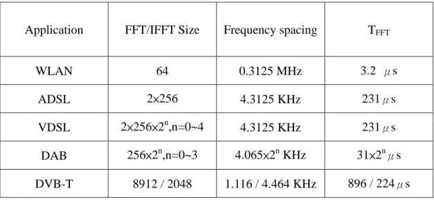
(12) Chapter 1. Introduction. 1.1 Introduction for Long-Length FFT. The fast Fourier transform (FFT) and inverse fast Fourier transform are key operations in modern communication systems, and the long-length FFT is commonly adopted in order to increase transmission bandwidth or efficiency, such as wireless LAN, ADSL, VDSL, and digital audio/video broadcasting systems, as shown in Table 1.1. By the growing trend towards longer length, FFT processors need more and more computing power, memory spaces, and hardware costs. There are many research works on short-length FFT processors have been done for several decades, but few on long-length FFT processors. There is still much space left for optimizing the implementations of long-length FFT.. 1.
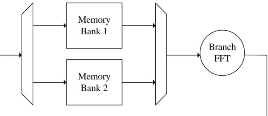
(13) Application. FFT/IFFT Size. Frequency spacing. TFFT. WLAN. 64. 0.3125 MHz. 3.2 μs. ADSL. 2×256. 4.3125 KHz. 231μs. VDSL. 2×256×2n,n=0~4. 4.3125 KHz. 231μs. DAB. 256×2n,n=0~3. 4.065×2n KHz. 31×2nμs. DVB-T. 8912 / 2048. 1.116 / 4.464 KHz. 896 / 224μs. Table 1.1 Various FFT applications. 1.2 Recursive Architecture Overview. In order to decrease the implementation complexity, recursive architectures are commonly used while structuring long-length FFT, as shown in Fig. 1.1. Radix-n Memory. Branch FFT. Fig. 1.1. Recursive architecture of radix-n FFT. 2.
(14) In such a recursive architecture, the first data of the current iteration can not be loaded into the “branch” FFT until the last data of the previous iteration is done. Thus, the latency of the branch FFT will be a performance bottleneck. An approach to lower the latency between the stages in recursive architectures is required for better performance. Furthermore, the faster calculations are finished up, the lower power is consumed. It is also a way to increase energy efficiency in the meanwhile. Numerous methods to optimize recursive architecture of long-length FFT were reported. In [11], a cache-memory architecture is adopted to enhance the performance of the memory system. A matrix prefetch buffer scheme is proposed in [12] that reorders the access of the memories between the stages in order to make sure the fluency of the dataflow because of the transposed order of the branch FFT. A COBRA FFT processor [10] uses an array architecture and is composed of multiple chips utilizing bit-serial arithmetic and dynamic reconfiguration. In this thesis, a study on algorithms and low-latency structures of short-length FFT for recursive long-length FFT is presented.. 1.3 Design for Optimized Structure. To solve the issues on latencies of branch FFT, a new structure featured in CORDIC (COordinate Rotation DIgital Computer) and DA (Distributed Arithmetic) techniques is proposed. With the property of bit-serial computations, this structure can run at a high frequency (max. 427MHz) with low latency (4 clock cycles). The absolute latency is 9.36 ns. However, for a 16 bit-parallel 8-point FFT computation, the latency increases to 20 clock cycles, and the absolute latency reaches 46.8 ns. Compared to the parallel 8-point FFT structure, the latter can run at max. 154MHz within 2 clock cycles of 3.
(15) latency. The absolute latency is only 12.94 ns. In the view of power dissipation, the proposed structure consumes about 41.6~59.1 mW (depends on the scalability of datapaths, will be described in later chapters) at 20MHz in average, but the straight structure consumes only 12mW. We expected a parallel 8-point FFT to be inferior to the proposed structure because of its long latency at the inter-stage complex multipliers. Apparently, the proposed structure gains no benefits in non-bit-serial computations. A study on this issue is presented in this thesis. All simulations are done with TSMC 0.18μm single-poly six-metal CMOS process.. 1.4 Organization of This Thesis. The following is the summary of each chapter.. Chapter 2. Backgrounds. The main idea of the thesis, including FFT algorithm, CORDIC, and DA, is discussed in this chapter. Then, various implementations of the short-length FFT are described. Some of them are chosen as implementing candidates.. Chapter 3. Short-length FFT. Because of the long latency inside the branch FFT, including 8-point FFT and the twiddle factor rotation, the performance of recursive architectures is limited. The characteristics of several conventional implementations are shown in this chapter.. Chapter 4. Long-length FFT. In order to solve the performance issues while adopting a short-length FFT in 4.
(16) recursive long-length FFT architectures, we looked for several methods to realize the branch FFT. A new implementation of the branch FFT with CORDIC and DA techniques is proposed.. Chapter 5. A Case Study: 802.11a wireless LAN 64-point FFT Processor. In order to verify the performance of the proposed architecture, several implementations of the 8-point branch FFT were developed. Then, two test chips are realized following the specification of the 802.11a wireless LAN 64-point FFT processor. The simulation results show that the parallel 8-point FFT is the best choice for implementing short-length FFT of recursive long-length FFT.. Chapter 6. Conclusion. Finally, we make a conclusion on our research works.. 5.
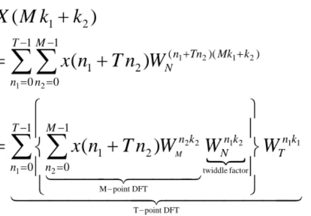
(17) Chapter 2. 2.1. Backgrounds. Discrete Fourier Transform. The N-point discrete Fourier transform (DFT) X(k) of a complex data sequence x(n) is defined as N −1. X ( k ) = ∑ x ( n )WNnk , k ∈ {0, 1, ..., N − 1} n =0. (1). where the twiddle factor is nk N. W. =e. − j(. 2π nk ) N. (2). If N is large, the number of MAC (Multiply and ACcumulate) operations described in (1) will be relatively large. Also, the multiplication required in (1) is a complex multiplication that consists of 4 real multiplications and 2 real additions. Decomposing (1) will help saving the computational costs. Let. N = MT ⎧n1 ∈ {0, 1, ..., T − 1} ⎨ ⎩n2 ∈ {0, 1, ..., M − 1} ⎧k ∈ {0, 1, ..., T − 1} k = M k1 + k 2 , ⎨ 1 ⎩k2 ∈ {0, 1, ..., M − 1} n = n1 + T n2 ,. Applying the values in (3), (1) can be reformed as. 6. (3).
(18) X ( M k1 + k2 ) =. T −1 M −1. ∑ ∑ x(n. n1 =0 n2 =0. 1. + T n2 )WN( n1 +Tn2 )( Mk1 + k2 ). ⎧ ⎫ ⎪ M −1 ⎪ = ∑ ⎨ ∑ x ( n1 + T n2 )WMn2k2 WNn1k2 ⎬ WTn1k1 { n1 =0 ⎪ n2 = 0 144424443 twiddle factor ⎪ − point DFT ⎩ 444M4 ⎭ 44 14 4 4244444 3 T −1. (4). T − point DFT. By the derivation described in (4), one long-length DFT operation can be decomposed into multiple short-length DFT operations with additional twiddle factor rotations. Considering N to be power of r, the N-point DFT can be decomposed into logrN stages of r-point DFT. This special case enables the availability of structuring recursive short-length DFT for long-length DFT. The computational complexity of (1) is O(N2). With the FFT algorithm, the computational complexity can be reduced to O(NlogrN) where r means that the radix-r FFT operations are utilized. Table 2.1 [17] shows the number of real additions and multiplications required for an N-point FFT.. Real Additions N. Radix-2. 8. 40. 16. 112. 32. 296. 64. 744. 128. 1800. 256. 4232. 512. 9736. 1024. 22024. 2048. 49160. Real Multiplications. Radix-4 Radix-8 Radix-2 Radix-4 Radix-8 52 155. 16 48. 4 27. 136 1011. 972. 360. 243. 204. 904 5635. 2184 12420. 28931. 1539. 5128 11784. 3204 8451. 26632. Table 2.1 Number of real additions and multiplications required for N-point FFT 7.
(19) For a 2-point and a 4-point FFT operation, the hardware can be implemented with only adders. An 8-point FFT operation can be implemented with adders and 1/√2 constant scalars which causes hardware complexity a little higher. However, it decreases the overall complexity more while adopted in long-length FFT operations. Since the radix-r FFT with an r higher than 8, such as radix-16, decreases the overall complexity even more, the complexity of the branch FFT is much higher because of the need of complex multipliers.. 2.2 Memory System Architectures. For a radix-r FFT algorithm, the hardware architecture of N-point FFT is decomposed into logrN stages with r-point branch FFT. Each stage requires reading and writing to N data words, and memory access is considered to be one of the bottlenecks under the recursive structure of long-length FFT. The followings are memory system architectures previously proposed.. 2.2.1 Single Memory This is the simplest architecture that only one memory bank is connected to the branch FFT, as shown is Fig. 2.1. Additional input and output buffers are required while adopted in a real-time FFT processing.. 2.2.2 Dual Memory In this architecture, shown in Fig. 2.2, two memory banks are functioned as a set of ping-pong buffer so that it is capable to real-time FFT processing. logrN times of iterations are required to complete an N-point FFT. Meanwhile, a clock rate higher than logrN times of the sampling rate is also required. 8.
(20) 2.2.3. Pipeline. In this architecture, the recursions are flattened. The computational resource costs are increased because of the requirements of logrN branch FFT and logrN+1 buffer memory, as shown in Fig. 2.3. On contrast, the clock rate is comparatively low as the same frequency of the sampling rate to meet real-time FFT processing.. 2.2.4 Array Processors using an array architecture consist of a series of independent processing elements, buffers, and a communication networks, as shown in Fig. 2.4. For example, the COBRA processor [10] contains an array of radix-4 butterfly processors, an 128-element I/O memory, an 128-element data-exchange block, and an 128×128 crossbar matrix.. Main Memory. Fig. 2.1. Branch FFT. Single-memory architecture block diagram. Memory Bank 1 Branch FFT Memory Bank 2. Fig. 2.2. Dual-memory architecture block diagram. 9.
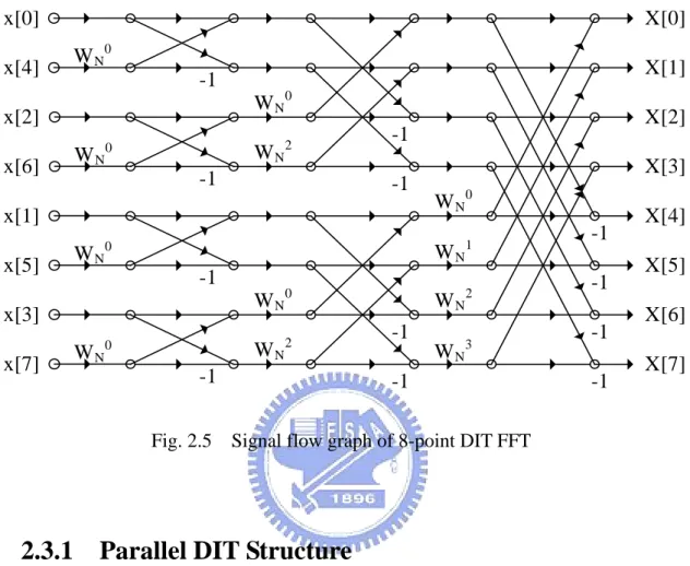
(21) Buffer Memory. Branch FFT. Buffer Memory. Branch FFT. .... Buffer Memory. Branch FFT. Fig. 2.3 Pipeline architecture block diagram. FFT PE. FFT PE. .... Communication Networks. Memory. Fig. 2.4. .... Memory. Array architecture block diagram. 2.3 8-point FFT Hardware Implementation. As shown in Table 2.1, a radix-8 FFT reduce the complexity more than other radix. Thus, it is chosen as the branch FFT for implementing long-length FFT in this thesis. There are many implementations have been proposed, such as radix-2 multi-path delay commutator (R2MDC) [30] and radix-2 single-path delay feedback (R2SDF) [21]. The FFT algorithm can be expressed in two forms, decimation in time (DIT) and decimation in frequency (DIF). Fig. 2.5 shows the signal flow graph of an 8-point DIT FFT. In this section, several 8-point FFT implementations in DIT form 10.
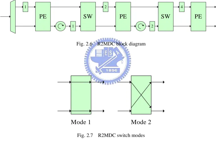
(22) will be introduced.. x[0]. X[0] W N0. x[4]. -1. x[2]. W N0. -1. -1. x[1] -1. x[3]. W N0. W N0. W N2 -1. W N2. W N0. x[7]. X[3]. W N1. W N0. x[5]. X[2]. -1. W N2. W N0. x[6]. X[1]. -1 Fig. 2.5. W N3. -1. -1 -1 -1 -1. X[4] X[5] X[6] X[7]. Signal flow graph of 8-point DIT FFT. 2.3.1 Parallel DIT Structure In this structure, the hardware is as Fig. 2.5 shown. Every component is directly mapped and realized. It is the straightest structure but costs the most area resource. However, by great parallelism, it calculates all 8 outputs at the same time within the least latency.. 2.3.2. Radix-2 Multi-path Delay Commutator (R2MDC). This is a direct implementation of radix-2 FFT algorithm using pipeline structure. Fig. 2.6 outlines the block diagram of R2MDC. At first, the MUX switches up, and the first data are loaded into the buffer. Then, the MUX switches down, the second 11.
(23) data passes through the path, the both operands of the first butterfly are ready, and the PE calculates the butterfly. The switches between stages operate in two modes, as shown in Fig. 2.7. In mode 1, the two inputs passes through; in mode 2, the inputs are swapped. With proper control, the switch can feed the right operands to next butterfly operation. In R2MDC, the utilization of the butterflies and delay buffers are 50% for each.. 1. 2. PE. SW. 4. PE. SW. 1. 2. Fig. 2.6. R2MDC block diagram. Mode 1 Fig. 2.7. Mode 2 R2MDC switch modes. 12. PE.
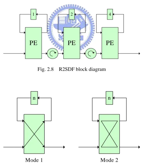
(24) 2.3.2 Radix-2 Single-path Delay Feedback (R2SDF) Since the utilization of buffers in R2MDC is only 50%, the R2SDF structure reduces its inter-stage buffer size by half. With feedback delay buffers, the utilization can reach 100%. Fig. 2.8 outlines the block diagram of R2SDF. In this structure, the PE holds two jobs: switching data and butterfly. Fig.2.9 shows the two operating modes of PE. In mode 1, the input data is passed to the buffer queue, and the data from the buffer is passed to the next stage with no modification; in mode 2, the PE calculates the butterfly from the input and the buffer, and the results are propagated to the next stage.. 1. 2. 4. PE. PE. PE. Fig. 2.8. R2SDF block diagram. n. n. Mode 1. Mode 2. Fig. 2.9. R2SDF operation modes 13.
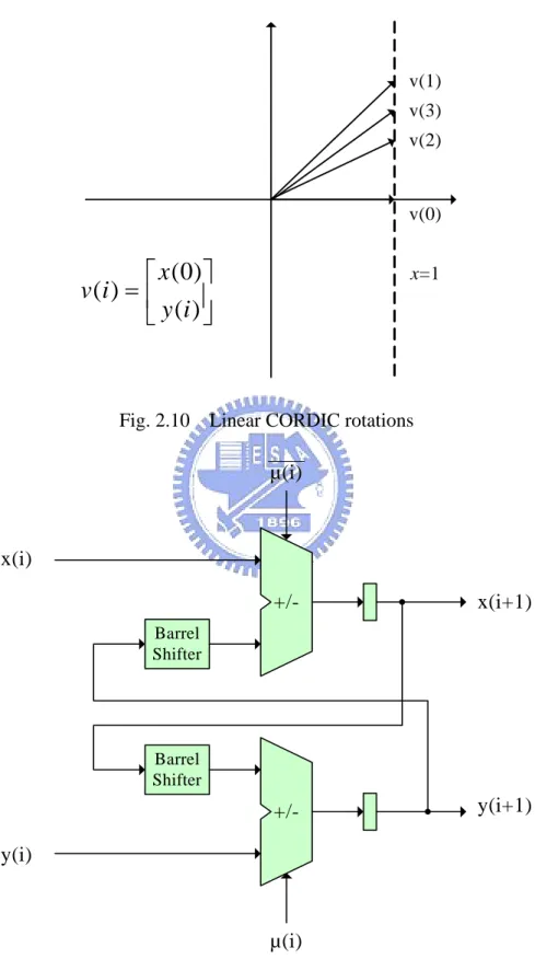
(25) 2.4 CORDIC Overview. The CORDIC (COordinate Rotation DIgital Computer) which was developed by Volder [26] in 1959 is an iterative arithmetic algorithm for phase rotation using a unified shift-add approach [2]. The concept of the CORDIC algorithm is to decompose the desired angle into weighted sum of a set of predefined elementary rotation angles such that the angles can be accomplished with simple shift-add operations. Fig. 2.10 is an example of the CORDIC algorithm with linear coordinate systems. Let the desired angle θ be represented as n −1. θ = ∑ μi a ( i ). (5). i =0. where μi represents the rotation signs conventionally with set {-1,1} and the i-th elementary rotation angle a (i) is defined as. a (i ) = tan −1 2 − i. (6). With the above definitions, the CORDIC algorithm can be described as an iterative equation as follows. ⎡ x (i + 1) ⎤ ⎡ 1 ⎢ y (i + 1)⎥ = ⎢ μ 2 −i ⎣ ⎦ ⎣ i. − μi 2 − i ⎤ ⎡ x ( i ) ⎤ ⎥ 1 ⎦ ⎢⎣ y (i )⎥⎦. (7). (7) shows a simple implementation of a CORDIC iteration with a shift-add structure, illustrated in Fig. 2.11. The elementary rotation angles described in (6) are not normalized while i >1. To make sure the final coordinate [xf yf]T is normalized, the scale factor K is defined as. ⎡xf ⎤ ⎡ x(n) ⎤ ⎢y ⎥ = K⎢ ⎥= ⎣ y ( n )⎦ ⎣ f⎦. 1 n −1. ∏ i =0. 14. 1 + μi2 2 −2 i. ⎡ x(n) ⎤ ⎢ y ( n )⎥ ⎣ ⎦. (8).
(26) where x(n) and y(n) are the output of the last iteration.. v(1) v(3) v(2). v(0). ⎡ x (0) ⎤ v (i ) = ⎢ ⎥ ⎣ y (i ) ⎦. Fig. 2.10. x=1. Linear CORDIC rotations. µ(i). x(i) +/-. x(i+1). +/-. y(i+1). Barrel Shifter. Barrel Shifter. y(i). µ(i) Fig. 2.11 Block diagram of basic single CORDIC iteration. 15.
(27) The basic CORDIC algorithm [2] can be described as follows:. Initiation: Given x(0), y(0), z(0). For i=0 to n-1, Do /* CORDIC iteration equation */. ⎡ x (i + 1) ⎤ ⎡ 1 ⎢ y (i + 1)⎥ = ⎢ μ 2 −i ⎣ ⎦ ⎣ i. − μi 2 − i ⎤ ⎡ x ( i ) ⎤ ⎥ 1 ⎦ ⎢⎣ y (i )⎥⎦. /* Angle updating equation */ z(i+1)=z(i)-μiam(i) End i-loop /* Scaling Operation */ ⎡xf ⎤ ⎡ x(n) ⎤ ⎢y ⎥ = K⎢ ⎥= ⎣ y ( n )⎦ ⎣ f⎦. 1 n −1. ∏ i =0. 1 + μi2 2 − 2i. ⎡ x(n ) ⎤ ⎢ y ( n )⎥ ⎣ ⎦. Generally, the rotation angle θ is known in many DSP applications. Thus, the rotation signs μi can be precomputed rather than online computation. The calculation is done by (7) and the value of is obtained as. ⎧ 1 if ⎩− 1 if. μi = ⎨. x (i ) ≥ 0 x (i ) < 0. (9). For a fixed number of CORDIC iterations i, the scale factor K will also be a constant. The redundant CORDIC proposed by Erocegovac and Lanf [22] is a modified version of the CORDIC method. In this algorithm, the rotation signsμi can be taken from the set {-1, 0, 1} instead of the set {-1, 1} defined as. 16.
(28) ⎧ if ⎪1 ⎪⎪ μi = ⎨0 if ⎪ ⎪− 1 if ⎪⎩. 2 i x (i ) ≥. 1 2. 1 1 > 2 i x (i ) > − 2 2 1 2 i x (i ) ≤ − 2. (10). if μi = 0 during this iteration, no computation is required. In this method, the computational costs of certain CORDIC iterations may be saved. However, these zero-rotation angles need no normalization because no rotations are completed as a matter of fact. Thus, it also causes variable scale factors. Many schemes are proposed to compensation the variable scale factors. A double rotation method [23] can reduce number of iterations while keeping constant scale factors. A differential CORDIC method [24] is proposed to implement redundant constant scale factor without correcting iterations. A prediction rotation method with the concept of Wallace tree, Booth encoding, and termination algorithm is proposed to speedup redundant addition while keeping a constant scaling factor [25]. Compared to complex-multiplier-based phase rotators, the standard CORDIC method possesses the advantage of smaller area, higher speed, and better capability for pipelined architecture, but pays longer latency because of its iterative mechanization. The redundant CORDIC method can avoid unnecessary computation while rotating the vectors so that latency will be reduced. But it also introduces the issues on variable scale factors and required additional devices to handle.. 17.
(29) 2.5. DA Overview. DA (Distributed Arithmetic) is a technique to calculate a sum of product more efficiently. Basically it is a bit-serial arithmetic algorithm. Considering an example of a sum of products: K. y = ∑ Ak xk k =1. (11). where Ak are fixed coefficients, and xk are the input data words. If xk is a 2’complement binary number, then it can be expressed as N −1. xk = − bk 0 + ∑ bkn 2 − n n =1. (12). where bkn is the bits, bk0 is the sign bit, and bkN-1 is the LSB. Replacing (11) with (12), one will get. ⎡K ⎤ y = − ∑ Ak bk 0 + ∑ ⎢∑ Ak bkn ⎥ 2 −n k =1 n =1 ⎣ k =1 ⎦ N −1. K. (13). Notice that whether bkn or bk0 only takes on values of 0 and 1, the bracketed term in (13): K. ∑Ab k =1. k kn. (14). has only 2k possible values. These values can be precomputed and stored in ROM rather than run-time computed. Thus, a ROM of lookup tables and a shift-add accumulator form the basic DA mechanization. The input data are fed from LSB to MSB in a bit-serial style, and the accumulator adds the value from LUT (LookUp Table) to the 1-bit right-shifted value of the previous accumulation. The accumulator changes its operating mode from an adder to a subtractor while the incoming bits are 18.
(30) the sign bits. Here is an example of a sum of product with 4-word input data, as shown in Fig. 2.12. The Ts control signal is asserted while the current bit-serial input is MSB, as sign bit, and the adder switches to the subtractor. DA is a very efficient means to computations that are dominates by inner products [4], especially for constant coefficients. Whenever the performance / cost ratio is critical, DA should be taken into consideration.. x1 x2 x3 x4. 1 1 1 1. 16-Word ROM. 1. ± Σ. Input Code b1n b2n b3n b4n. Parallel Output Ts. Sign Control 0 = Add 1 = Subtract. +. Barrel Shifter. Fig. 2.12 DA mechanization of 4-word input data. 19. 0 0 0 0 0 0 0 0 1 1 1 1 1 1 1 1. 0 0 0 0 1 1 1 1 0 0 0 0 1 1 1 1. 0 0 1 1 0 0 1 1 0 0 1 1 0 0 1 1. 0 1 0 1 0 1 0 1 0 1 0 1 0 1 0 1. 16-word Memory Contents 0 A4 A3 A3+A4 A2 A2+A4 A2+A3 A2+A3+A4 A1 A1+A4 A1+A3 A1+A3+A4 A1+A2 A1+A2+A4 A1+A2+A3 A1+A2+ A3+A4.
(31) Chapter 3. Short-Length FFT. 3.1 Introduction. In the previous chapter, the radix-8 FFT algorithm and recursive architecture are described. In the recursive architecture, the first data of the current iteration can not be loaded into the branch FFT until the last data of the previous iteration is done. Thus, the timing delay between stages under such a recursive architecture is limited by the latency of branch FFT processors. As the number of iterations grows, a branch FFT with lower latency will result in a faster completion. Besides, under the same specification, an architecture, which completes calculations sooner, will stay in sleep longer and save more power. Therefore, a low latency branch FFT is required for a recursive architecture long-length FFT. The latency of branch FFT is mainly composed of two parts: 8-point FFT and inter-stage twiddle factor rotations. In this chapter, the objective is to resolve issues about latency in 8-point FFT, and the proposed 8-point FFT structure with CORDIC and DA technique is described. Issues about twiddle factor rotation are left for later chapters. All simulations are done with TSMC 0.18μm single-poly six-metal CMOS process.. 20.
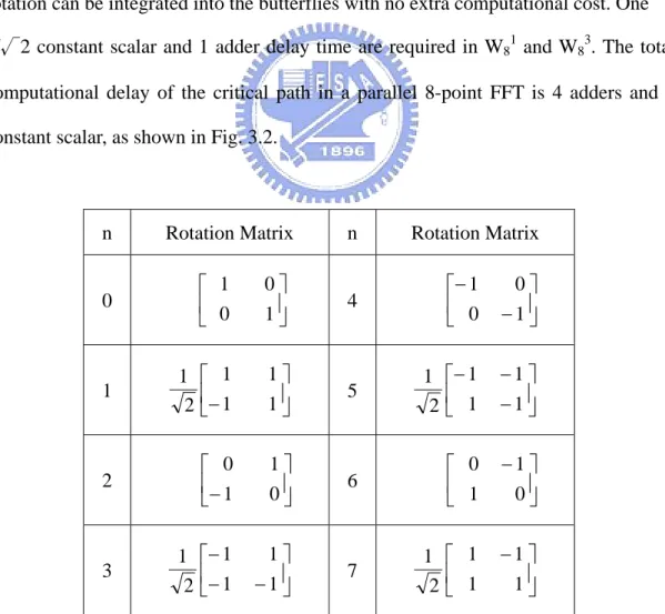
(32) 3.2 Latency in 8-point FFT. Consider a straight parallel 8-point FFT implementation. Each radix-2 butterfly operation produces 1 adder delay time. Table 3.1 shows the rotation matrix of W8n twiddle factors. Only W81, W82, and W83 are performed in an 8-point FFT. W80 does no computations and can be ignored. Fig. 3.1 shows a W82 rotation following a butterfly operation. The lower output signal B’ can be reformulated as: B' = [( AR − BR ) + j ( BI − AI )] × ( − j ) (15). = ( AI − BI ) + j ( BR − AR ). This modification can be done by simply swap the operands of subtractions. Thus, the rotation can be integrated into the butterflies with no extra computational cost. One 1/√2 constant scalar and 1 adder delay time are required in W81 and W83. The total computational delay of the critical path in a parallel 8-point FFT is 4 adders and 1 constant scalar, as shown in Fig. 3.2.. n. Rotation Matrix. 0. 1. 1 2. 2. 3. 1 2. n. Rotation Matrix. ⎡ 1 ⎢ 0 ⎣. 0⎤ 1 ⎥⎦. 4. ⎡− 1 ⎢ 0 ⎣. 0⎤ − 1 ⎥⎦. ⎡ 1 ⎢− 1 ⎣. 1⎤ 1 ⎥⎦. 5. 1 ⎡− 1 ⎢ 2⎣ 1. −1 ⎤ − 1 ⎥⎦. ⎡ 0 ⎢− 1 ⎣. 1⎤ 0 ⎥⎦. 6. ⎡ 0 ⎢ 1 ⎣. −1 ⎤ 0 ⎥⎦. ⎡− 1 ⎢− 1 ⎣. 1⎤ − 1 ⎥⎦. 7. 1 ⎡ 1 ⎢ 2⎣ 1. −1 ⎤ 1 ⎥⎦. Table 3.1 Rotation matrix of W8n 21.
(33) A. A' -j. B. x. -. B'. W82 rotation following a butterfly. Fig. 3.1. X[0]. x[0] x[4]. X[1]. -1. x[2] -j. x[6]. X[2]. -1. -1. X[3]. -1. x[1] W8. x[5]. 1. -1. -1. -j. x[3]. -1. -j. x[7]. W8. -1. Fig. 3.2. -1. 3. -1. -1 -1. X[4] X[5] X[6] X[7]. Critical path in an 8-point DIT FFT. 3.3 CORDIC-DA Structure. The FFT algorithm saves the computational costs because it makes use of dependencies between stages of radix-2 FFT operations. However, the dependencies become a source of latency while being implemented into hardware. Considering the original DFT definition shown in (1), a DFT operation is intrinsically a sum-of-product operation. For an 8-point DFT, the latency is the delay time of one 2-operand adder, one 8-operand adder, and one constant scalar. If there is an implementation with a better approach to summations and constant scaling, the latency can be reduced. The proposed CORDIC-DA structure may possibly reach this goal. 22.
(34) An 8-point DFT is defined as 7. X [k ] = ∑W8nk x[n ] n =0. (16). where W8nk is the twiddle factor. Implementing the twiddle factor with CORDIC method, (16) can be expressed as. ⎡ Re{ X [k ]}⎤ 7 ⎡ Re{x[n ]}⎤ ⎢ Im{X [k ]}⎥ = ∑ K ( n, k ) M 2×2 (n, k ) ⎢ Im{x[n ]}⎥ ⎣ ⎦ n =0 ⎣ ⎦ ⎧ 1 if n and k are both even ⎪ K ( n, k ) = ⎨ 2 ⎪⎩1 otherwise. (17). where K(n,k)M2x2(n,k) is the rotation matrix shown in Table 3.1. In the view of the redundant CORDIC method, K(n,k) is the scale factor of CORDIC, and M2x2(n,k) is the pure additions of CORDIC. There are 2 CORDIC iterations: π/2 rotation and tan-11 rotation. Notice that certain twiddle factors in () require no tan-11 rotation, thus the scale factor K(n,k) has two possible values: 1 and 1/√2, as described in (17), and is a variable scale factor. The concept of the CORDIC-DA structure is that the CORDIC stage processes rotations without scale factor; the DA stage handles the variable scale factor and summation.. 23.
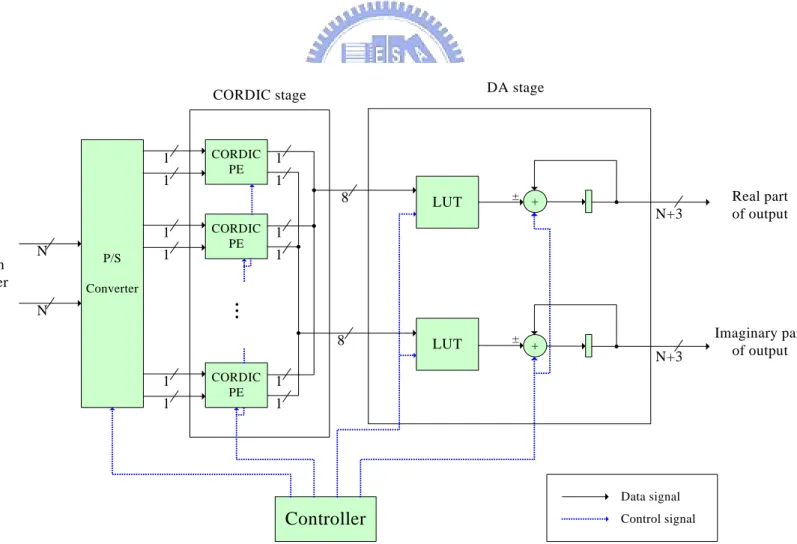
(35) The block diagram of the proposed structure is illustrated in Fig. 3.3. It is a pipelined 8-point FFT processor. There are 3 stages, the P/S converter (Parallel-to-Serial converter), the CORDIC stage, and the DA stage. Between the CORDIC stage and the DA stage, there exists a series of pipeline registers that separate the two stages. The P/S converter contains total 16 sets of N-bit shift registers, 2 sets for real and imaginary part each operand. They load 8 data words from the memory buffer, outputs the LSB to the DA stage, and then right shift 1-bit in next cycle. The shift operation is a circular shift that the MSB in next cycle will be the content of the LSB in previous cycle. Because shift operations consume heavy power, a ‘shift’ control signal is designed to control the right shift operation. When the pipeline is inactive, the right-shift operation will be stopped.. DA stage. CORDIC stage. 1 1. CORDIC PE. 1 1 8. 1 N From Buffer. P/S. 1. CORDIC PE. LUT. ± +. LUT. ±. N+3. Real part of output. N+3. Imaginary part of output. 1 1. .... Converter. N. 8 1 1. CORDIC PE. +. 1 1. Data signal. Controller. Control signal. Fig. 3.3 Block diagram of 8-point CORDIC-DA FFT 24.
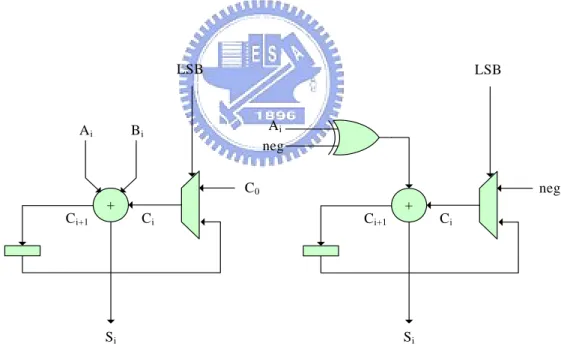
(36) Originally, the P/S converter is placed in front of the DA stage. However, if the P/S converter is moved behind the CORDIC stage, the CORDIC PE can be utilized with bit-serial arithmetic that extremely saves the cell area. For example, if a 16-bit adder is transformed into a 1-BAAT (Bit At A Time) bit-serial adder, only 1-bit adder and few flip-flops are required, as shown in Fig. 3.4. When ‘LSB’ signal is asserted, an external carry-in signal C0 is transmitted to the carry-in of the full adder, otherwise the carry-out of the previous cycle stored in the register is transmitted. It computes sum like a RCA (Ripple-Carry Adder) does, but in a bit-serial style. Theoretically, N cycles are required to complete a bit-serial CORDIC computation for N-bit input. An extra 1-bit guard bit is added in order to prevent from overflow thus total N+1 cycles are required.. LSB. Ai. LSB. Ai neg. Bi. C0. neg. + C i+1. +. Ci. Si. Fig. 3.4. Ci. Ci+1. Si. (a) 1-BAAT bit-serial adder (b) 1-BAAT 2’s complementor. 25.
(37) The CORDIC stage is composed of a CORDIC PE array, as shown in Fig. 3.5. Total 8 CORDIC PEs are required for an 8-point FFT. Fig. 3.5 shows the block diagram of the CORDIC PE. Each PE consists of 4 OR gates, 4 bit-serial 2’s complementors, and 2 bit-serial adders. There is a controller that centralizes the control signals which are independent of each other. With proper control signals shown in Table 3.2, the PEs can implement all W8n rotations shown in Table 2.1, except the 1/√2 scaling.. ctrl [2] ctrl [0] Real part of input. 1. 1. 2's complmentor. 1. +. ctrl [1] Imaginary part of input. 1. 1. 2's complmentor. 1. Real part of output. 1. Imaginary part of input. 1. ctrl [3] ctrl [6] ctrl [4] 1. 2's complmentor. 1. +. ctrl [5] 1. 2's complmentor. 1. ctrl [7]. Fig. 3.5. CORDIC PE block diagram. 26.
(38) Twiddle factor Control signal ctrl[0..7] W80. 0 0 1 0 0 0 0 1. W81. 0 1 1 1 0 0 1 1. W82. 0 1 0 1 0 0 1 0. W83. 1 1 1 1 0 1 1 1. W84. 1 0 1 0 0 1 0 1. W85. 1 0 1 1 1 1 1 1. W86. 0 0 0 1 1 0 1 0. W87. 0 0 1 1 1 0 1 1. Table 3.2 CORDIC PE control signal mapping. After rotation, the outputs from the CORDIC stage, which are bit-serial styled, are transmitted to the address line of the LUT (LookUp Table) in the DA stage. There are two sets of LUT and accumulator that handle the real part and imaginary part of the processing data individually. Basically, the lookup table sums all inputs up, and scales 1/√2 if this input channel needs to:. ⎡ X ( 0) ⎤ ⎢ X (1) ⎥ ⎢ ⎥ ⎢ X ( 2)⎥ ⎢ ⎥ ⎢ X ( 3) ⎥ = ⎢ X ( 4)⎥ ⎢ ⎥ ⎢ X (5) ⎥ ⎢ X ( 6) ⎥ ⎢ ⎥ ⎣ X (7)⎦. ⎡W80 ⎢ 0 ⎢W8 ⎢W80 ⎢ 0 ⎢W8 ⎢W80 ⎢ 0 ⎢W8 ⎢W 0 ⎢ 80 ⎣⎢W8. W80 W81. W80 W82. W80 W84. W80 W85. W80 W86. W86 W80 W81 W84 W84 W80. W82 W87 W84. W84 W82 W80. W85 W86. W82 W87 W84 W84 W82 W80. W81 W86. W86 W84. W87. W86. W84 W83. W82. W82 W84 W83 W86 W84 W80. W80 W83. W85. W80 ⎤ ⎡ x ( 0) ⎤ ⎥ W87 ⎥ ⎢⎢ x (1) ⎥⎥ W86 ⎥ ⎢ x ( 2 ) ⎥ ⎥⎢ ⎥ W85 ⎥ ⎢ x ( 3) ⎥ W84 ⎥ ⎢ x ( 4 ) ⎥ ⎥⎢ ⎥ W83 ⎥ ⎢ x (5) ⎥ W82 ⎥ ⎢ x ( 6) ⎥ ⎥⎢ ⎥ W81 ⎦⎥ ⎣ x ( 7 ) ⎦. (18). where the shaded coefficients contain a 45-degree rotation and need to be scaled. The address bus width of the LUT is 11 bits, including 8-bit data input and 3-bit iteration index term that loops from 0 to 7 while computing 8-point DFT, and a 27.
(39) 2K-word ROM is required. It is large number that is hard to implement and need to be modified. Actually, the sum operation can be calculated with an ones counter which simply counts the number of the logic ‘1’ from the 8-bit input so that the address line can be decreased to 4 bits. Besides, as (14) shown, only the odd channel is possibly to be scaled by 1/√2. As shown in Table 3.3, according to the combination of each CORDIC channel output, there are 25 possible values. This is a small-size ROM, thus it is realized with synthesized logic rather than real ROM module. The modified LUT architecture is shown in Fig. 3.6, if the current iteration contains 45-degree rotations, the data passes 1’s counter, remapping table, and LUT, otherwise it passes 1’s counter only.. # of 1/√2 # of 1. 0. 0. 0. 0.707107 1.414214 2.121320 2.828427. 1. 1. 1.707107 2.414214 3.121320 3.828427. 2. 2. 2.707107 3.414214 4.121320 4.828427. 3. 3. 3.707107 4.414214 5.121320 5.828427. 4. 4. 4.707107 5.414214 6.121320 6.828427. 1. 2. 3. 4. Table 3.3 The 25 words used in LUT. CORDIC output. 8. 1s counter. 4. Address Remapping Table. 5. Reduced 25-word coefficient ROM. N. 3. Index term. LUT. Fig. 3.6. Block diagram inside the modified LUT. 28. To DA accumulator.
(40) Assume the input data width is N bits. Because an 8-point FFT is an 8-operand addition, total N+3 bits are required at the output. In the accumulator, a register of at least N+4 bits is required. The N+3 bits in MSB are necessary to hold the result, and the 1 bit in LSB is left for the accuracy while doing right-shift operations. One can increase the number of bit is LSB to gain more accuracy. In the test chip described in Chapter 5, a total 23 bits is utilized for 16-bit inputs. The latency of the proposed 8-point FFT structure depends on its data width because of the shift-accumulate operation in the DA stage. Total N+4 clock cycles are required to complete an 8-point FFT calculation. For a 16-bit FFT, the latency is 20 cycles, and it is a large number.. 3.3 Error Analysis. In the case of FFT hardware implementation, the finite bitwdith must be considered because of the fixed-point computation. Many statistical error analysis papers on FFT implementations are proposed [27-29]. However, the CORDIC-DA structure proposed in this thesis is not a traditional FFT implementation, and an extended error analysis has to be done to choose a suitable bitwdith for the datapath. Assume the input sequence of FFT x(n) is a sequence of finite-valued and white complex numbers. The variance of x(n) can be expressed as. σ x2 =. 1 N. N −1. ∑ ( x[n] − μx )2 = n =0. 1 N. N −1. ∑ ( x[n]) n =0. 2. (19). where μx is the mean of x(n) andμx =0. The SQNR (Signal-to-Quantization Noise Ratio) is defined as. σ x2 SQNR = 2 σq. (20). where σx2 is the variance of output andσq2 is the variance of the quantization error. 29.
(41) For an N-point FFT processor with input of which real and imaginary parts are uniformly distributed in ( −. 1 1 N, N ) , the variance [28] of the output is 2 2. 1 3N. σ X2 =. (21). From (20) and (21), the SQNR [29] of the conventional FFT implementation can be carried out:. SQNRFFT =. 22 B 5 N − 4m − 3. (22). where B is the bitwidth of the input sequence and m=log2N.. LUT. +. x[n]. CORDIC stage. X. eL. +. +. eA Accumulator stage. Fig. 3.7. Error model of CORDIC-DA. Fig. 3.7 shows the error model of CORDIC-DA. In the CORDIC stage, one more guard bit is added and can proof noise-free. The coefficients stored in the LUT are precomputed and rounded into M-bit that a roundoff noise eL is added. Because of the mechanism of DA, total B times shift-add operation will be done in the accumulator for a B-bit input sequence. The variance of the roundoff error until the accumulator is 30.
(42) 2 −2 M LUT 3 1 B −1 2 2 2 2 σ 1 = ( 2 ) σ LUT + ( 12 ) B −2 σ LUT + ... + ( 12 )0 σ LUT. σ2 =. B −1. 1 k k =0 2. 2 = σ LUT ∑. (23). 2 = 2(1 − 2 − B )σ LUT 2 ≈ 2σ LUT = 23 2 −2 M. At the end of the CORDIC-DA, the output will be rounded into B-bit. The variance of the rounding error is. 2 −2 B σ = 3 2 2. (24). From (23) and (24), the SQNR of the CORDIC-DA can be expressed as. SQNRCORDIC − DA. σ x2 = 2 σ 1 + σ 22 =. 1 1 ⋅ −2 M N 2⋅2 + 2 −2 B. (25). To increase SQNR, we would like to make M and B as large as possible but are limited by the implementation resource. A better decision on M and B is to make sure. 2 ⋅ 2 −2 M = 2 −2 B M = B + 0.5. (26). From (26), M=B+1 is a better solution for trade-off between resource usage and SQNR performance. Replace M=B+1 and N=8 in (22) and (26), the SQNR expressions can be rewritten as. SQNRFFT SQNRCORDIC − DA. 22 B = 25 22 B = 12. (27) (28). From (27) and (28), one can discover that the SQNR performance of the CORDIC-DA structure is better than the conventional implementation in the same 31.
(43) bitwidth. To match the SQNR of the two structure, we can lower the B and M value of the CORDIC-DA structure that will reduce the hardware cost. Concretely, to lower the M value is to decrease the bitwidth of the LUT, and to lower the B value is to decrease the registers of the accumulator and the remaining bits after roundoff. Table 3.4 lists the statistical SQNR analysis of the two structures. Although the CORDIC-DA structure performs better than the conventional FFT, there is no just match value on SQNR versus bitwidth. In the test chip, B=16 and M=16 is chosen.. 8 B 68.37 FFT CORDIC-DA 74.75. 9 80.41 86.79. 10 11 12 13 14 15 16 92.45 104.49 116.54 128.58 140.62 152.66 164.70 98.83 110.87 122.91 134.95 146.99 159.03 171.08. Table 3.4 Statistical SQNR analysis of conventional FFT and CORDIC-DA. 3.4 Implementation and Simulation Results. Since the 8-point CORDIC-DA FFT algorithm is proposed, an evaluation model is developed to verify the algorithm. The three FFT models: CORDIC-DA FFT, R2SDF FFT, and fully parallel FFT, are structured with 16-bit data width, and the clock constraints are set to very high frequency so that the limit of these implementations will be carried out. Table 3.5 lists the simulation results of these FFT implementations. The parallel FFT is a straight implement of 8-point DIT FFT, as shown in Fig. 2.5. There is no pipeline register used thus it requires only 1 clock cycle to complete an 8-point FFT operation. The R2SDF is implemented with Fig. 2.6. Because of the feedback registers, it requires 7 clock cycles to carry out the first result. The CORDIC-DA structure can run at a very fast speed because of the bit-serial arithmetic. However, the latency is affected by the data width, and it requires more clock cycles 32.
(44) to carry out the first result. According to the simulation results, the parallel FFT requires most area costs but shortest latency. On contrast, the CORDIC-DA structure utilized least area costs, but the latency is the longest of the three FFT implementations. It may possibly because of the long data width that the DA stage requires more clock cycles to accumulate. Although it can achieve very high frequency, it is still not fast enough. The critical path of CORDIC-DA is found on the LUT which is hard to be pipelined. The power consumption of the proposed CORDIC-DA structure is higher than the other two implementations. In order to achieve very high clock rate, the logic synthesizer inserted as much clock buffers as possible so that more power is consumed with the high toggle rate of the clock propagation. The result does not go as we expected so that an idea of merging the twiddle factor rotators into the branch FFT comes out. In this way, the latency produced by the twiddle factor rotator may be eliminated with little delay in our CORDIC-DA structure. However, if a serial I/O interface is adopted, the CORDIC-DA will possess the shortest latency. The shift-out bit in the accumulator can be passed to the serial output so that the first bit can be carried out in 2 clock cycle. The shortest clock period of CORDIC-DA structure is 1.65 ns, and the shortest latency is about 3.30 ns.. 33.
(45) Implementation. Parallel FFT. R2SDF. CORDIC-DA. 6.47 ns. 5.47 ns. 1.65 ns. 154.6 MHz. 182.8 MHz. 606.0 MHz. 23946. 10740. 9982. Clock cycle. 1. 7. 20. Timing. 6.47 ns. 38.3 ns. 33 ns. Throughput Rate (clock cycle). 0.125. 1. 17. Static power analysis. 66 mW. 42 mW. 24 mW. 3.77 mW. 6.65 mW. 35.6 mW. @ 20 MHz. @ 20 MHz. @ 400 MHz. Max. clock rate Gate count Latency. Simulation-based power analysis Table 3.5 Simulation results of short-length FFT. 34.
(46) Chapter 4. Long-Length FFT. 4.1 Introduction. There are two key components structuring recursive architecture long-length FFT: the short-length FFT (also known as the branch FFT) and the twiddle factor rotator. In the previous chapter, the objective of the proposed CORDIC-DA structure is to decrease the latency in the branch FFT. A modification to integrate the twiddle factor into the DA LUT will be described in this chapter. The memory architecture of the recursive FFT is another issue. In a recursive long-length FFT architecture, the frequent access to intermediate memory requires a high-speed memory device and efficient access scheme. A matrix buffer memory access scheme and how it is adopted in the memory devices provided by TSMC 0.18 μm CMOS process will be described in this chapter, too.. 35.
(47) 4.2. Memory Access. Consider a radix-8 FFT. One may replace M=8 in (4) and get. X (8k1 + k2 ) =. N 8. −1 7. ∑ ∑ x(n1 + N8 n2 )WN 1. ( n + 8 n2 )( 8 k1 + k 2 ) N. n1 =0 n2 = 0. ⎧ ⎫ 7 ⎪ ⎪ = ∑ ⎨ ∑ x ( n1 + N8 n2 )W8n2k2 WNn1k2 ⎬ W Nn1k1 { 8 n1 =0 ⎪ n2 =0 144424443 twiddle factor ⎪ point DFT ⎩ 4448−4 ⎭ 44 14 4 4244444 3 N 8. −1. (29). N − point DFT 8. Notice that the access order of the input and output between two iterations are the transpose of each other. For example, a 64-point FFT requires two iterations, and equipped with an 8 × 8 memory. At the first iteration, the output is stored to memory row by row, as shown in Fig. 4.1(a). At the second iteration, the input is loaded from memory column by column, as shown in Fig. 4.1(b). However, if the computation of the first column is completed, and the result is written back to buffer row by row, the operands of later 8-point FFT will be overwritten. To solve this problem, an addition buffer is required. But it increases area cost very much, and is not realizable. A matrix buffer scheme is proposed in [12] and solves this problem. The memory device is specialized that the access to columns and rows will be swapped for each iteration so that no operands will be overwritten.. 36.
(48) Column. Row. Write direction Read direction. (a). Column. Row. Write direction Read direction. (b) Fig. 4.1. Memory access collision between two stages. The matrix buffer is synthesized with cell-based process. In general, a synthesized memory device usually costs more area and power than a full-custom one. The TSMC 0.18μm CMOS process provides several memory generators, such as 37.
(49) single-port SRAM, dual-port SRAM, single-port register file, dual-port register file, etc. These hard-macro modules are good at area, timing, and power consumption compared to a synthesized one. We found that dual-port register file module is suitable for this access scheme, and a N-word register buffer is adopted in the recursive architecture.. 4.3 Latency in Twiddle Factor Rotator. There are many methods to implement twiddle factor rotators, such as complex multipliers, CORDIC, etc. A complex multiplier produces delay time of 1 real multiplier and 1 real adder. Delay time produced by a CORDIC rotator depends on the resolution of the elementary rotation angle derived from (6). One single CORDIC iteration stage produces delay of 1 real adder. For a N-stage CORDIC, total N real adder and one constant scalar delay are produced. The idea of the proposed new structure is to decrease the latency of the branch FFT iteration as possible. In our view, merging the twiddle factor rotation into the branch FFT is an alternative approach to lower the latency. Because of the LUT in DA, the twiddle factor rotation can also be precomputed and stored in the ROM with reasonable increase on ROM size and little additional logic.. 4.3.1 Complex Multiplier Phase Rotator A straight implementation of a phase rotator is complex multipliers as shown in Fig. 4.2. The critical path passed through a real multiplier and a real adder. The real part and imaginary part of the twiddle factors are constants, and can be stored in a ROM, as shown in Fig. 4.3. In practice, only a range of π/4 will be realized, as 38.
(50) shown in Fig. 4.4. The twiddle factors located at area II, III, IV, V, VI, VII, and VIII can be obtained from the ones located at area I with simply exchanging signs or/and exchanging real/imaginary part of operands. Table 4.1 shows the transform function. For example, for a 64-point FFT, total 9 coefficients of W640~W648 need to be stored in ROM. Other angles ranging from W649~W6463 can be obtained from the 9 angles.. Re[X(k)]. X. Im[X(k)]. cos. − sin. -. Real part of output. +. Imaginary part of output. X. 2π nk N. X. 2πnk N. X. Fig. 4.2. Signal flow chart of a complex multiplier. Coefficient ROM. X(k). Fig. 4.3. To next iteration. Configuration of coefficient ROM and phase rotator. 39.
(51) VI. VII. V. VIII. IV. I III. Fig. 4.4. Transform. II. The range of stored angles in practice. Index. Area. Transform. Index. Matrix. complement. Area Matrix. complement. I. ⎡ 1 ⎢ 0 ⎣. 0⎤ 1 ⎥⎦. No. V. ⎡ −1 ⎢ 0 ⎣. 0⎤ − 1 ⎥⎦. No. II. ⎡ 0 ⎢ −1 ⎣. −1 ⎤ 0 ⎥⎦. Yes. VI. ⎡ 0 ⎢ 1 ⎣. 1⎤ 0 ⎥⎦. Yes. III. ⎡ 0 ⎢ −1 ⎣. 1⎤ 0 ⎥⎦. No. VII. ⎡ 0 ⎢ 1 ⎣. −1 ⎤ 0 ⎥⎦. No. IV. ⎡ −1 ⎢ 0 ⎣. 0⎤ 1 ⎥⎦. Yes. VIII. ⎡ 1 ⎢ 0 ⎣. 0⎤ − 1 ⎥⎦. Yes. Table 4.1 The Transform Matrix within range of π/8. 40.
(52) 4.3.2 ROM Multiplier Phase Rotator A Basic ROM multiplier is utilized with a ROM which simply stores the products of the multiplication. For example, a ROM multiplier for N-bit multiplicand and M-bit multiplier requires a ROM with size of 2(N+M)×(N+M). However, a ROM multiplier realization becomes impractical while N or M is large. An alternative approach is to partition the data width into lower number of bits, and uses a shift-accumulator to accumulate the products. As shown in Fig. 4.5, the N-bit multiplicand is partitioned by every 4 bits, and right-shifts one block per cycle. The ROM stores the (4+M)-bit product of the 4-bit multiplicand and the M-bit multiplier. Then, the previous result stored in the accumulator is right-shifted by 4-bit, and is summed up with the product provided by ROM. The multiplication requires N/4 cycles to complete. As the lower bits the data is going to be partitioned, the more clock cycles to complete a multiplication are required.. 41.
(53) Multiplicand N. 0 1 0 0. .... 4. 1 1 0 1 0 1 0 0. 24+M-word Product ROM. N bits shift register. M. Multiplier 4+M. +. N+M. 4-bit Barrel Shifter. Fig. 4.5. 4BAAT ROM multiplier mechanism. In a basic ROM multiplier phase rotator, multipliers shown in Fig. 4.2 are simply replaced with ROM multipliers. Because the twiddle factor ROM stores constant coefficients, it can be merged into these ROM multipliers. For example, a ROM multiplier that multiplies a K-bit input with L possible fixed-point coefficients of twiddle factors WN1~L is shown in Fig. 4.6. The input passes through a series of shift registers which provides 4 bit per cycle to the ROMs. ROM A stores the product related to the real parts of WN1~L, and ROM B stores the product related to the real parts of WN1~L. The rotation will be complete after K/4 cycles.. 42.
(54) LUT A Real part of input. K. 4. 4BAAT shift register. +. Real part of output. +. Imaginary part of output. LUT B. LUT A Imaginary part of input. K. 4. 4BAAT shift register. LUT B. Rotating angle index. Fig. 4.6. 4.3.3. log2L. 4BAAT phase rotator with constant rotating angle. CORDIC-DA Structure with Phase Rotator. As the configuration described in Chapter 3, the ROM stores only few patterns because there are only two possible coefficients: 1 and 1/√2. DA is intrinsically a ROM-based multiplier. Considering a CORDIC-DA 8-point FFT processor following a twiddle factor rotator implemented with complex multipliers, the LUT can take advantages of the property of ROM-multiplier that combines the original function with the twiddle factor rotations. Moreover, the transform described in Fig. 4.4 can also be merged with the CORDIC with no extra computation. For example, a radix-8 branch FFT for 64-point FFT derived from (1) can be expressed as. T ( n1 , k2 ) =. 7. ∑ x(n. 1. n2 = 0. + 8n2 )W8n2k2. (30a). X (8k1 + k2 ) = ∑ {T ( n1 , k2 )W64n1k2 }W8n1k1 7. n1 =0. where T(n1,k2) is the intermediate data between stages. Let 43. (30b).
(55) nˆ = n1k2 mod 8 ⎢n k ⎥ kˆ = ⎢ 1 2 ⎥ ⎣ 8 ⎦. (30c). (16b) can be rewritten as. X (8k1 + k2 ) = ∑ { T ( n1 , k2 ) W64nˆ }W8n1k1 + k 7. ˆ. (30d). n1 =0. which extracts the W8 elements from W64n1k2 . Thus, the W8 rotation, which has been integrated with the CORDIC stage, can be skipped in LUT. Fig. 4.7 shows the block diagram of the refined CORDIC-DA FFT structure.. DA stage. CORDIC stage. 1 1. CORDIC PE. LUT A. 1 1. 1 Nx8. P/S. CORDIC PE. Real part of output. N+3. Imaginary part of output. LUT B. 1 1. Converter. .... From Buffer. 1. N+3. ± +. 8. Nx8. LUT A 8 ± +. 1 1. CORDIC PE. 1. LUT B. 1. Data signal. Controller. Control signal. Fig. 4.7 Block diagram of the refined CORDIC-DA FFT. 44.
(56) 8. 1s counter. CORDIC output. 6 4. 1s counter. 2 scale flag. 4. 2N Remapping table 1. Index term. 2N. 8. 8. 1. 64-word LUT. 3. 2-word LUT. To DA accumulator. 2N. LUT. Fig. 4.8. Block diagram of integrated LUT for 64-point FFT. The complex multipliers of the twiddle factor rotation are replaced with four LUTs. Each LUT maps to the real multiplier shown in Fig. 4.2. The LUT A stores the product of input and cos. sin. 2π nk , and The LUT B stores the product of input and N. 2π nk . Although in Fig.4.7 LUT A and B are separated, the content of the two N. LUT are actually integrated in a single ROM in realization so that the bitwidth of the output will be 2N bits. Fig. 4.8 illustrates the block diagram of the integrated LUT for 64-point FFT. There are two control signals: 1/√2 scaling flags and new ‘index term’ signal. Because of the W8 extraction described in (16d), every CORDIC PE has had the ability to handle a 45-degree-based rotation, thus a new 1/√2 scale flag is designed to instruct the LUT to scale the designated input channel individually. The ‘index term’ control signal is different from the old one. In the refined structure, the ‘index term’ signal is directed from the nˆ described in (30c) which is calculated in the controller. Considering the output of the two ones counter and index term, the content of the LUT can be expressed as. ⎧( a − b) + bWNnˆ x=⎨ ⎩0 45. if a ≥ b otherwise. (31).
(57) where x is the output of LUT, a is the result from the ones counter of the CORDIC output, and b is the result from the ones counter of logic AND operation between the CORDIC output and 1/√2 scale flag. a and b range from 0 to 8, and a<b will never occur so that a value of zero is filled. In the case of 64-point FFT, nˆ ranges from 0 to 7, and total 36×8 words are required to store all LUT contents. However, there are two problems to implement the LUT: this number is not power of 2, and the remapping logic shown in Fig. 4.8 will be complex that produces longer latency. During the synthesis process, the most critical path is found at the LUT stage, thus the latency in this stage needs to be short as possible. A trade-off solution is adopted that splits the LUT into 2 sub-LUTs, a 64-word one and a 2-word one. The 64-word LUT stores the content of a=1~7 and b=1~7, as expressed in (31). The address is simply concatenated from the 3-bit LSB from the result of ones counters. a=0,b=0, and a=8, b=8, are seen as special cases, and are handled by the 2-word LUT. In these special cases, the final output of the LUT stage is switched to the 2-word LUT, or switched to the 64-word LUT otherwise. The accumulator in the DA stage is modified into a 3-operand adder. It is implemented with a CSA (Carry-Save Adder) and adds delay of a 3-input XOR gate to the critical path. With the integration, little delay on the critical path is attached but the twiddle factor rotators are all saved. This refined CORDIC-DA branch FFT may possibly gains more benefits while utilized in a recursive architecture long-length FFT.. 4.4 Implementation and Simulation Results. Although the synthesized 8-point CORDIC-DA FFT structure can run at a very high frequency, the clock is hard to propagate. An in-chip PLL (Phase-Locked Loop) 46.
(58) circuit may solve this problem. A PLL circuit requires a low frequency external clock source and can generate a high frequency internal clock source. However, we have no such PLL models. Another approach that increases the number of datapath in CORDIC-DA is adopted. The CORDIC-DA FFT computes one result of 8-point FFT at a time, thus increasing the datapath will help produce more results at a time. As shown in Fig. 4.9, a complete datapath, which is called a ‘channel’, includes a CORDIC stage and a DA stage. The P/S converter can be shared by channels so that it is not duplicated. The implementations follow the specification described in the previous chapter. A set of CORDIC-DA structures with 1, 2, 4, 8 pipes are developed, and they are already capable of twiddle factor rotation. The other two implementations, R2SDF and parallel FFT, are developed with a complex multiplier twiddle factor rotator shown in Fig. 4.2. According to the synthesis report listed in Table 4.2, we discovered that CORDIC-DA FFT could achieve better power efficiency while more pipes are utilized. With higher working frequency, more power consumes on the clock buffers, and driving ability of logic cells is strengthened so that more power is required. Compared to the basic 8-point CORDIC-DA FFT without merging twiddle factor rotators, the critical path increases to about 2.4 ns because of the growing LUT size. However, they still spent more latency than the other two conventional FFT implementations. Unexpectedly, the optimization effort on the complex multiplier done by the logic synthesizer is very high. As the report shown, the 16×16 multiplier produced very low delay that is less than 5.4 ns. Notice the two measurements of power density listed in Table 4.2. The “power density” is how much power consumed per K gate counts at the same throughput rate. A higher value somehow means a better area efficiency. As the result shown, the 1-channel version of CORDIC-DA possesses the highest area efficiency, and verifies 47.
(59) the previous inference. The “normalized power” is how much power consumed per MHz working frequency, not the same throughput rate. A higher value somehow means a higher toggle rate, or utilization on physical circuits. According to the reported values, this value is proportion to the number of channels. This value of the 1-channel CORDIC-DA structure is low, but the total power consumption is higher than the CORDIC-DA configured with more channels. The high power consumption is possibly is possibly because of the high clock rate that more power is consumed by the clock propagation. If a full serial environment is considered that the I/O interfaces and memory buffers are configured in bit-serial arithmetic, the latency of the CORDIC-DA will still be the shortest of these FFT implementations. As described in the previous chapter, only 2 clock cycles are required to carry out the first bit.. channel 0 CORDIC stage. LUT. ACC. channel 1 CORDIC stage. From memory. LUT. ACC. P/S Converter. N-word buffer. ... channel N-1 CORDIC stage. LUT. ACC. Fig. 4.9 Duplicate datapaths in CORDIC-DA stage. 48. To memory.
(60) CORDIC-DA. Parallel. Structure. R2SDF FFT. 1 channel 2 channels 4 channels 8 channels 2.34 ns. 2.36 ns. 2.41 ns. 2.50 ns. 5.47 ns. 6.47 ns. Max. clock rate 427.4 MHz 423.7 MHz 414.9 MHz 400.0 MHz 182.8 MHz. 154.6 MHz. Clock cycle. 20. 20. 20. 20. 8. 2. Timing. 46.8 ns. 47.2 ns. 48.2 ns. 50 ns. 43.8 ns. 12.9 ns. 14,792. 25,142. 44,922. 81,852. 25,666. 36,394. Latency. Gate count Static power analysis. 52.9 mW @ 52.2 mW @ 55.8 mW @ 49.1 mW @ 7.2 mW @ 400 MHz. 200 MHz. 100 MHz. 50 MHz. 20 MHz. 4.84 mW @ 20 MHz. Simulation-based 59.1 mW @ 51.5 mW @ 45.8 mW @ 41.6 mW @ 18.1 mW @ 12.0 mW @ power analysis Power density (mW / K gates) Normalized power (mW / MHz). 400 MHz. 200 MHz. 100 MHz. 50 MHz. 20 MHz. 20 MHz. 4.00. 2.05. 1.02. 0.51. 0.71. 0.33. 0.15. 0.26. 0.46. 0.83. 0.905. 0.6. Table 4.2 Summary of branch FFTs. 49.
(61) Chapter 5. A Case Study: 802.11a. Wireless LAN 64-Point FFT Processor. 5.1. Design Environment. In the previous chapters, the proposed CORDIC-DA structure is described. An FFT test chip for long-length application is developed to verify the proposed FFT processor. This test chip follows the specification of 802.11a wireless LAN 64-point FFT processor. According to the results shown in the previous chapters, the parallel 8-point FFT implementation is better than the proposed structure at power and speed. Thus, another test chip is also developed with the parallel 8-point FFT implementation to verify the argument. The specified FFT processor is a 16-bit 64-point FFT processor, working at the sampling frequency of 20 MHz. The proposed architecture was modeled in VHDL and functionally verified using Mentor Graphics’ Modelsim simulator. After functional validation, the processors were synthesized for TSMC 0.18μm single-poly six-metal CMOS technology using Synopsys Design Compiler. After synthesis, floor planning, P&R, and layout were carried out using Cadence SOC 50.
(62) Encounter, as shown in Fig. 5.1 and Fig. 5.2. Finally, the post-simulation power analysis on the netlists exported from SOC Encounter is carried out using Synopsys PrimePower.. Fig. 5.1 Layout view of 64-point FFT with CORDIC-DA structure. 51.
(63) Fig. 5.2 Layout view of 64-point FFT with parallel FFT structure. 5.1.1. Clock Issues. At first, the 1-channel version with dual-memory architecture is developed, as shown in Fig. 5.3. A 64-point FFT operation can be completed within 2 iterations. The 1-channel version requires 20 cycles to complete one result so that total 20×64=1280 cycles are required for each iteration. With extra cycles spent on memory access, a total number of over 2560 cycles is required to complete a 64-point FFT operation. An average of more than 40 cycles is required per output at 20 MHz. Thus, a very high 52.
(64) frequency clock source of over 20×40=800 MHz is required. Considering the clock source generation, this implementation is impractical. Notice that no twiddle factor rotation is needed during the second FFT iteration. Thus, the second 8-point FFT processing unit can be structured with no phase rotator. Considering the unbalanced computational requirement of the 2 branch FFTs, the 2 iterations can be structured individually. Separating them into 2 pipeline stages will help decreasing the area costs and lowering the clock rate by less than a half. Although the study is concentrated on recursive architectures, the high clock rate makes the chips hard to realize. The chips have to be implemented with frequency about 200MHz or even lower thus a flattened architecture is needed. A refined version with flattened pipeline architecture was built, as shown in Fig. 5.4. The second stage is structured with 8-point parallel DIT FFT. Switch Input buffer. Input port 32. 32. 1-word buffer. Switch Output buffer. 64-word dual-port register file 0. Output port. 64-word dual-port register file 1. 32. 32. 32. 8-word buffer. 32. 256. CORDIC-DA FFT. 32. Fig. 5.3 Block diagram of 1-channel version CORDIC-DA FFT with recursive architecture. Input buffer. Input port 32. 32. 64-word dual-port register file 0. 32. 8-word buffer. 256. 1-pipe CORDIC-DA FFT. 32. 1-word buffer. 32. 64-word dual-port register file 1. 32. 8-word buffer. 256. 8-point parallel FFT. 256. 8-word buffer. 32. 64-word dual-port register file 2. Fig. 5.4 Block diagram of CORDIC-DA with 2 pipeline stages. 53. Output buffer. Output port 32. 32.
(65) According to the bad performance result, we tried to develop a 2-channel version of CORDIC-DA FFT. As the result described in the previous chapter, the 2-channel version is better at power consumption and clock frequency, thus we developed a VHDL model which is parameterized on number of channels with the GENERIC statement. Available options are 1, 2, 4, 8 channels, and clock rates are 400, 200, 100, 50 MHz respectively. Considering power consumption and area costs, the 4-channel version was chosen to realize. In these designs, two clock domains are adopted: the bit-serial domain and bit-parallel domain. The bit-serial domain, in which the circuits work at 1:1 frequency as the external clock source, contains the CORDIC-DA FFT and the P/S converter. The other components are of the bit-parallel domain, in which the circuits work at 20MHz, and the clock source is supplied by in-chip digital clock divider.. 5.2. Verification. A functional test environment was built using Matlab which generates random test patterns for verification, as shown in Fig. 5.5. The testbench compares the simulation results to the golden patterns, which were also generated by Matlab, and run-time analyzes PSNR (Peak Signal-to-Noise Ratio) which is defined as: MSE =. 1 N. N −1. ∑ (Result (n) − Golden(n) ). 2. n =0. ⎛ 2b ⎞ ⎟⎟ PSNR = 20 log10 ⎜⎜ ⎝ MSE ⎠. where N is the number of the point of FFT and b is the bitwidth of data bus.. 54. (32).
數據
+7
相關文件
volume suppressed mass: (TeV) 2 /M P ∼ 10 −4 eV → mm range can be experimentally tested for any number of extra dimensions - Light U(1) gauge bosons: no derivative couplings. =>
For pedagogical purposes, let us start consideration from a simple one-dimensional (1D) system, where electrons are confined to a chain parallel to the x axis. As it is well known
The observed small neutrino masses strongly suggest the presence of super heavy Majorana neutrinos N. Out-of-thermal equilibrium processes may be easily realized around the
Define instead the imaginary.. potential, magnetic field, lattice…) Dirac-BdG Hamiltonian:. with small, and matrix
incapable to extract any quantities from QCD, nor to tackle the most interesting physics, namely, the spontaneously chiral symmetry breaking and the color confinement..
(1) Determine a hypersurface on which matching condition is given.. (2) Determine a
• Formation of massive primordial stars as origin of objects in the early universe. • Supernova explosions might be visible to the most
The difference resulted from the co- existence of two kinds of words in Buddhist scriptures a foreign words in which di- syllabic words are dominant, and most of them are the
