between the on-package PIFA and the radio-frequency (RF) components in the shielding package was studied. The antenna performance rarely changes and the isolation between the antenna and the RF components can be maximized when the locations of the components are appropriately arranged in the package. Finally, a wireless local-area network (WLAN) front-end module (FEM) including the switch, low-pass filter (LPF), bandpass filter (BPF), and power amplifier (PA), is embedded into the shielding package of the antenna. The error vector magnitude (EVM) of the resultant antenna integrated FEM, together with a WLAN card containing the baseband/medium-access control (MAC) circuitry, is tested. Good performance is obtained, showing the usability of the proposed antenna configuration.
Index Terms—Antenna, planar inverted-F antenna (PIFA), system-on-package (SOP), wireless local-area networks (WLAN).
I. INTRODUCTION
T
HE WLAN has been one of the most important appli-cations of wireless communication technology in recent years. The wireless local-area networks (WLAN) standards have been developed by the Institute of Electrical and Elec-tronics Engineers (IEEE) and the 802.11 standard is a family of specifications for WLAN technology. For instance, WLAN in the 2.4-GHz band (2.40–2.4835 GHz) of IEEE 802.11b/g has been developed widely and rapidly applied by using wireless communication terminals, such as desktop computers, laptop computers, mobile phones, personal digital assistants (PDAs), etc. Recently, many conventional antennas have been success-fully designed for wireless applications, such as monopole antenna, planar inverted-F antenna (PIFA), patch antenna, and dielectric resonator antenna (DRA) [1]–[7].Manuscript received November 2, 2006; revised January 22, 2007. This work was supported in part by the National Science Council, R.O.C., under Contract NSC 95-2752-E-009-003-PAE and the Computer and Communica-tions Research Laboratories of Industrial Technology Research Institute (ITRI), Hsinchu, Taiwan , R.O.C.
C.-W. Ling and S.-J. Chung are with the Department of Communication En-gineering, National Chiao Tung University, Hsinchu, Taiwan 30050, R.O.C. (e-mail: [email protected]).
C.-Y. Lee was with the Department of Communication Engineering, National Chiao Tung University, Hsinchu, Taiwan, R.O.C. He is now with the Chi Mei Communication Systems Incorporation, Taipei, Taiwan, R.O.C.
C-L. Tang is with Auden Techno. Corp., Taoyuan, Taiwan, R.O.C. Color versions of one or more of the figures in this paper are available online at http://ieeexplore.ieee.org.
Digital Object Identifier 10.1109/TAP.2007.898640
the antenna’s ground. The system ground-plane dimensions, to some extent, can strongly affect the antenna impedance band-width. And the other kind of DRA is attracted the attention of antenna researchers because of its wide impedance bandwidth and flexible coupling schemes [4]. Another kind of antenna de-sign is PIFA that provides several merits of compact size, light weight, and low cost [5]–[7].
Nowadays, system-on-package (SOP) technology is one so-lution for establishing future wireless transceiver modules that can provide flexibility by integrating all functional blocks using the multilayer process and novel interconnection methods. Many single-chip wireless transceivers have been designed, such as those fabricated in 0.25 m at 1.8 GHz for DCS-1800 applications and at 2.45 GHz for Bluetooth applications [8]. To enhance the function of SOP for wireless communications, it has become very attractive to develop the SOP which is efficient in integrating an antenna with a module. In the case that the embedded antennas are integrated with the low-temperature co-fired ceramic (LTCC) package, semiconductor substrates, or the ceramic ball grid array package (CBGA), interferences between the antenna and the radio-frequency (RF) blocks may happen in highly integrated modules [9]–[15]. Usually, the patch antenna is employed and stacked on the top above the circuit within the package. The configuration leads to an increase in the overall height of the package and result in narrowband operation as well. In addition, due to the use of high-permittivity dielectric material, the radiation efficiency of the antenna is also limited.
In this study, an on-package PIFA, consisting of a single folded metal plate for WLAN applications, is proposed. Fab-ricating an antenna directly on the package has the advantage of reducing feeder loss and the overall size of the circuitry. The shielding package can perform as part of the ground plane and block to eliminate the undesired coupling with nearby RF components. The proposed antenna achieves an impedance bandwidth of 6.55% from 2.37 to 2.53 GHz, with dimensions of 20 mm 15 mm 3.5 mm. Additionally, the coupling effect between the on-package PIFA and the RF components in the shielding package is examined. The antenna performance is rarely changed and the isolation between the antenna and the RF components can be maximized by appropriately locating the components in the package.
Section II presents the geometry and design of the on-package PIFA. Section III investigates the coupling effects between the on-package PIFA and the RF components. Section IV
Fig. 1. Geometry of the on-package PIFA. (a) Three–dimensional (3-D) struc-ture. (b) Side view ofx–z plane. (c) Side view of y–z plane.
ments and demonstrates the integration of an on-package PIFA and WLAN front-end module. Finally, Section V presents conclusions.
II. CONFIGURATION ANDDESIGN
In this study, the PIFA is integrated with a package using a single folded metal plate. Since the antenna is to satisfy the specification of IEEE 802.11b/g WLAN, the required return loss bandwidth should cover the band 2.4–2.4835 GHz. The on-package PIFA is implemented on the FR4 substrate, whose dielectric constant is 4.4, loss tangent is 0.02, and thickness is 0.8 mm.
Fig. 1 shows the three–dimensional (3-D) structure and side views of the on-package PIFA. The length and width of the on-package PIFA determine the resonant frequency, which is approximated by the formula
(1) where is the velocity of light; and are the length and width of the radiating element, and is the resonant frequency. The radiating element is connected to the ground by using a
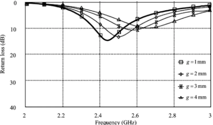
Fig. 2. Return loss of on-package PIFA with various gap widths between the shorting strip and the feed strip;` 2 w = 14.5 mm 2 15 mm, ` 2 w = 15 mm2 20 mm, W 2 L = 20 mm 2 40 mm, h = 1.5 mm, and s = 0 mm.
short-circuit strip located near the antenna’s feed strip. Equation (1) yields the patch size of the antenna 14.5 mm 15 mm and an overall physical length of approximately one quarter-wavelength at the desired frequency of 2.45 GHz. The size of the shielding package is and the ground size is . The feed point is denoted as point as shown in Fig. 1.
The antenna is integrated with the shielding package using a single folded metal plate. The shorting strip is located at the corner of the patch and the feed of the on-package PIFA is lo-cated at the edge of the shielding package. The width and height of the shorting strip are 1.5 and 2 mm, respectively, while those of the feed strip are 1.5 and 3.5 mm, respectively. The input impedance of the antenna can be easily matched to 50 by controlling the feed position relative to the shorting strip. The proposed antenna structure is simulated using Ansoft high-fre-quency structure simulator (HFSS) [16], a commercial 3-D full-wave electromagnetic (EM) simulation software. Fig. 2 shows the return losses with various gap widths between the shorting strip and the feed strip. The dimensions of the radiating ele-ment, the shorting strip, and the feed strip are fixed. The ground size and shielding package sizes are also specified as
20 mm 40 mm and 20 mm 15 mm, respectively. When the gap width is smaller, input impedance matching can be improved. However, an extremely small gap width cannot be realized practically. Thus, the restriction of the fabrication technology must be considered and then the gap between the shorting strip and the feed strip chosen as 1 mm.
The effect of the position of the shorting strip on antenna performance is investigated. All of the antenna dimensions are fixed, except for the shorting strip position relative to the shielding package sidewall. The center frequency increases as the shorting strip moves along the direction (i.e., becoming farther from the sidewall), because the equivalent current length decrease as increases. In Fig. 3, the impedance bandwidth ex-ceeds that required for the IEEE 802.11b/g WLAN band appli-cation when is 0 mm. Furthermore, the shorting strip is located at the corner of the shielding package, indicating that the feed strip is adjacent to the shielding package sidewall. Accordingly, the vertical current on the feed strip would not readily excite the
Fig. 3. Return loss of on-package PIFA with various shorting strip positions. Other geometric parameters are the same as given in Fig. 2.
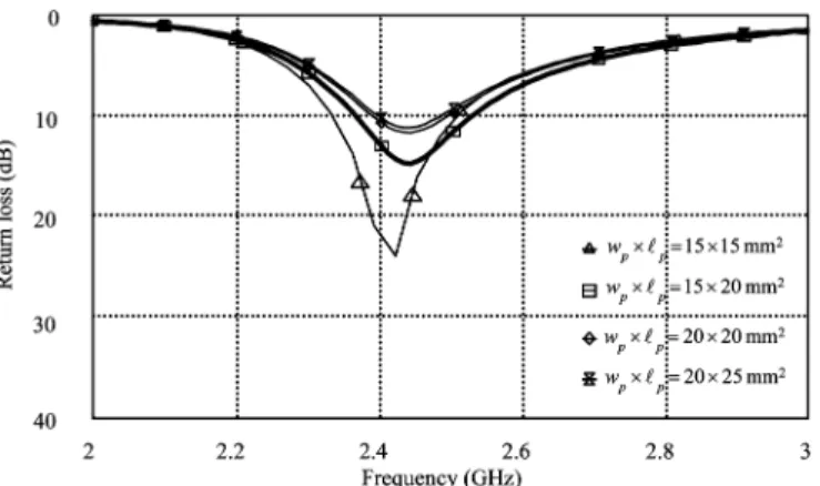
Fig. 4. Return loss of on-package PIFA with various shielding package sizes. Other geometric parameters are the same as given in Fig. 2.
cavity mode in the shielding package. Another advantage is that the size is small for a given operating frequency.
The RF components can be placed within the shielding package and the baseband circuits arranged outside. The ground size and shielding package change with the size of the circuitry. However, the ground size influences the antenna performance and the shielding package is one part of the on-package PIFA. Therefore, changing the ground size and the shielding package affects the characteristics of the on-package PIFA. Hence, it is interesting to see the effect of varying the shielding package and the ground length.
Fig. 4 shows the simulated return losses for various shielding package sizes, including 15 mm 15 mm (case 1), 20 mm 20 mm (case 2), and 20 mm 25 mm (case 3). The result for the original package size (15 mm 20 mm) is also shown for comparison. Basically, the antenna frequency is changed little due to the variation of the package size. The bandwidth of case 1 exceeds the original, but those in the other two cases are worse.
The other parameter of shielding package is the package height. Fig. 5 shows the effect of the package height on the re-turn loss, with 1.5, 2, 2.5, and 3 mm. The input impedance bandwidth is rarely changes with the package height, and the input impedance matching is improved when the package height exceeds the original value 1.5 mm . It has been observed from the simulation result that the input reactance
Fig. 5. Return loss of on-package PIFA with various shielding package heights. Other geometric parameters are the same as given in Fig. 2.
Fig. 6. Return loss of on-package PIFA with various ground lengths. Other geometric parameters are the same as given in Fig. 2.
of the on-package PIFA with 1.5 mm is capacitive. In-creasing the package height would lengthen the feed strip, thus increasing the input inductance. Therefore, a larger package height is associated with better input matching. Hence, the proposed on-package PIFA is appropriate for RF components of various height without redesign when the package height is increased from 1.5 to 3 mm.
The effect of ground length is also examined. The ground width is fixed to 20 mm and the ground length varied among 35, 45, and 50 mm. Fig. 6 shows the input return loss in each case. It is seen that the return loss at ground length of 35 mm is much poor, due to the truncation of the induced ground current.
As mentioned earlier, the proposed antenna structure can be made using a single metal sheet. As illustrated in Fig. 7, first, trim the shape of the on-package PIFA and bend downward three sides of the shielding package except the one nearby the feed strip. Then bend upward the antenna patch, followed by bending the last side of the package. To keep the spacing be-tween the antenna patch and the shielding package so as to re-main the antenna performance, a low-loss foam with relative dielectric constant near 1.0 can be inserted in between. Fig. 8 compares the simulated and measured input return losses of the proposed antenna for package and ground sizes of
15 mm 20 mm 1.5 mm and 20 mm 40 mm, re-spectively. A total impedance bandwidth of 160 MHz from 2.37
Fig. 7. Manufacture procedure of on-package PIFA.
Fig. 8. Measured and simulated return loss of on-package PIFA.` 2 w = 14.5 mm2 15 mm, ` 2 w = 15 mm 2 20 mm, W 2 L = 20 mm 2 40 mm, h = 1.5 mm, g = 1 mm, and s = 0 mm.
Fig. 9. Illustration of BPF locations.` 2 w = 15 mm 2 20 mm.
to 2.53 GHz is measured. Good agreement between the mea-sured and simulated results is obtained.
III. COUPLING BETWEENON-PACKAGEPIFAAND
RF COMPONENTS
The vertical current on the feed strip of the on-package PIFA would radiate field into the shielding package through the aper-ture on the package’s sidewall. This might induce the coupling between the antenna and the RF components embedded in the package. It is thus interesting to check the coupling level be-tween the on-package PIFA and the components. Essentially, the RF circuitry comprises a T/R switch, filters, a power ampli-fier (PA), and an RF transceivers [17]–[20]. Here, for simplicity, an LTCC bandpass filter (BPF) is adopted to represent a typical
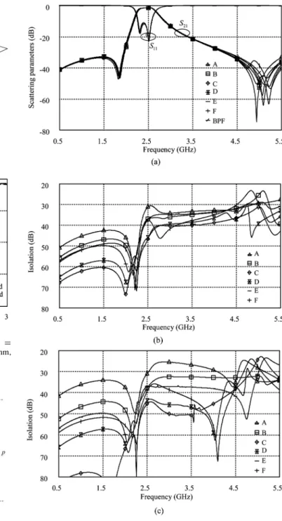
Fig. 10. Simulation results of the scattering parameters with BPF at various locations. (a) Return loss(0S ) and insertion loss (0S ) of the BPF. (b) Isolation(0S ) between ports 1 and 3. (c) Isolation (0S ) between ports 2 and 3. The geometrical parameters are the same as given in Fig. 8.
RF component. Since the layout of the LTCC BPF formed with inductors and capacitors was known, it is thus possible to ana-lyze the coupling effect using the EM software HFSS.
The BPF with size of 2.5 mm 2.0 mm 1 mm is arranged at six locations (denoted from A to F) inside the package as shown in Fig. 9. Ports 1 and 2 are the input and output ports of the BPF, while port 3 represents the input port of the on-package PIFA. Locations E and F are at the same position, but with the BPF rotated 90 . Fig. 10(a) shows the simulation return loss and insertion loss of the BPF at various locations. The results for the BPF without the package are also shown for com-parison. It is seen that the performance of the BPF is not changed
Fig. 11. Return loss of the on-package PIFA with BPF integrated. The geo-metric parameters are the same as given in Fig. 8.
with the location. The insertion loss in the passband keeps under 2 dB. Fig. 10(b) and (c) depicts the simulation isolations ( and ) between the antenna port and the two BPF ports. First of all, it is seen that the isolations are all better than 30 dB in the passband. This high-isolation level benefits the avoidance of signal oscillation, especially when a high-gain amplifier is embedded in the package. More close observation reveals that as the component is placed in front of the antenna port (location A), the coupling is highest. When the component is moved to the far end, such as locations C and D, the isolation can be greatly improved to be better than 45 dB in the passband. Although not shown here, it has been checked that the return loss response of the on-package PIFA does not change due to the placement of the BPF.
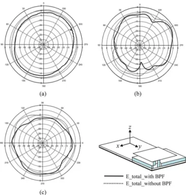
With the BPF placed at location B and the output port con-nected to the input of the on-package PIFA through a 50- mi-crostrip line, a one-port antenna with BPF integrated is obtained. Fig. 11 illustrates its simulated and measured return losses as functions of frequency. Both curves well agree with each other and have three poles, two from the BPF and one from the an-tenna. The measured radiation patterns at the three principal planes are presented in Fig. 12. Those of the antenna without the BPF are also shown for comparison. The patterns are quite omnidirectional, especially in the - plane. The peak gains (av-erage gains) for the BFP integrated antenna are 1.34 3.38 , 1.68 5.30 , and 1.30 5.12 dBi in the , , and -planes, respectively. Due to the insertion loss of the BPF, the gains are about 2 dB lower than those of the antenna without BPF embedded.
IV. INTEGRATION OFON-PACKAGEPIFAANDWLAN FRONT-ENDMODULE
The designed on-package PIFA was integrated with the WLAN front-end module (FEM), forming an antenna em-bedded front-end module (AFEM). Fig. 13 shows the block diagram of the module. The FEM includes a T/R switch (SW), an LTCC low-pass filter (LPF), an LTCC BPF, and a PA. Table I lists the specifications of these RF components. The FEM was first built and measured. The results reveal that in the passband, the insertion loss on the RX path is 2.72 dB and the signal gain on the TX path is 25.83 dB. Both are chosen to the ideal values
Fig. 12. Radiation patterns of the on-package PIFA with and without BPF at 2.45 GHz for (a)x-z plane, (b) y-z plane, and (c) x-y plane. The geometric parameters are the same as given in Fig. 8.
Fig. 13. Block diagram of on-package PIFA integrated with WLAN front-end module and WLAN card.
TABLE I
THESPECIFICATIONS OFEACHCOMPONENT IN THEWLAN FRONT-ENDMODULE
(2.51 and 26.63 dB, respectively) calculated from Table I. The fabricated FEM was placed inside the package of the antenna, with the switch output connected to the antenna input. To form a complete WLAN unit, we used cables to connect the TX and RX ports to a commercial WLAN card, which contains a RF transceiver and the baseband/medium-access control (MAC) circuitry.
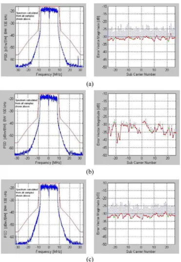
Fig. 14(a)–(c) shows the test results of the error vector magnitude (EVM) and spectrum masks. The test distance is 3 m between the transmitter and the receiver antennas. The EVM is 30.99, 32.51, and 31.29 dB at 2.412, 2.442 and 2.472 GHz, respectively. All of these values are under 25 dB, which is the maximum EVM specified by the IEEE 802.11g.
Fig. 14. Test results of the EVM and spectrum masks at (a) 2.412 GHz, (b) 2.442 GHz, and (c) 2.472 GHz.
Fig. 15. Photograph of the antenna embedded front-end module (AFEM) and a WLAN card.
Also, the spectra are well controlled under the mask. Fig. 15 shows the photograph of the circuit for testing.
V. CONCLUSION
An on-package PIFA made from a single folded metal plate for IEEE 802.11b/g WLAN band applications has been pro-posed and demonstrated. The prototype has a compact size of 15 mm 20 mm 3.5 mm. Several design parameters, such as
REFERENCES
[1] Y.-Y. Wang and S.-J. Chung, “A new dual-band antenna for WLAN applications,” in Proc. IEEE AP-S Int. Symp., Jun. 20–25, 2004, vol. 3, pp. 2611–2614.
[2] M. N. Suma, P. C. Bybi, and P. Mohanan, “A wideband printed monopole antenna for 2.4-GHz WLAN applications,” Microwave Opt. Technol. Lett., vol. 48, pp. 871–873, May 2006.
[3] C.-M. Su, K.-L. Wong, W.-S. Chen, and Y.-T. Cheng, “A mi-crostrip-coupled printed inverted-F monopole antenna,” Microwave. Opt. Technol. Lett., vol. 43, pp. 470–472, Dec. 2004.
[4] A. V. P. Kumar, V. Hamsakutty, J. Yohannan, and K. T. Mathew, “Microstripline-fed half-cylindrical dielectric resonator antenna for 2.4-GHz WLAN application,” Microwave. Opt. Technol. Lett., vol. 48, pp. 724–726, Apr. 2006.
[5] H. Park, K. Chung, and J. Choi, “Design of a planar inverted-F antenna with very wide impedance bandwidth,” IEEE Microwave and Wireless Compon. Lett., vol. 16, pp. 113–115, Mar. 2006.
[6] Y.-B. Kwon, J.-I. Moon, and S.-O. Park, “An internal triple-band planar inverted-F antenna,” IEEE Antennas Wireless Propag. Lett., vol. 2, pp. 341–344, 2003.
[7] F. Wang, Z. Du, Q. Wang, and K. Gong, “Enhanced-bandwidth PIFA with T-shaped ground plane,” Electron. Lett., vol. 40, pp. 1504–1505, Nov. 2004.
[8] M. Steyaert, M. Borremans, J. Janssens, B. Muer, I. Itoh, J. Cran-inckx, J. Crols, E. Morifuji, S. Momose, and W. Sansen, “A single-chip CMOS transceiver for DCS-1800 wireless communications,” in Proc. IEEE Int. Solid-State Circuits Conf., Feb. 5–7, 1998, pp. 48–49. [9] K. Lim, A. Obatoyinbo, M. Davis, J. Laskar, and R. Tummala,
“Development of planar antennas in multi-layer packages for RF system-on-a-package applications,” Electrical Perform. Electron. Package, pp. 101–104, Oct. 2001.
[10] Y. P. Zhang, “Finite-difference time-domain analysis of integrated ceramic ball grid array package antenna for highly integrated wireless transceivers,” IEEE Trans. Antennas Propag., vol. 52, no. 2, pp. 435–442, Feb. 2004.
[11] Y. P. Zhang, “Integrated circuit co-fired laminated ceramic package an-tenna,” in Proc. IEEE Int. Solid-State and Integrated-Circuit Technol. Conf., Oct. 22–25, 2001, vol. 1, pp. 101–103.
[12] Y. P. Zhang, “Integrated circuit ceramic ball grid array package an-tenna,” IEEE Trans. Antennas Propag., vol. 52, no. 10, pp. 2538–2544, Oct. 2004.
[13] Y. P. Zhang, “Integration of microstrip antenna on cavity-down ce-ramic ball grid array package,” Electron. Lett., vol. 38, pp. 1307–1308, Oct. 2002.
[14] Y. P. Zhang, “Design of on-package microstrip antennas for single-chip wireless transceivers,” in Proc. IEEE Electron. Packag. Technol. Conf., Dec. 10–12, 2002, pp. 40–44.
[15] C. T. P. Song, P. S. Hall, and H. Ghafouri-Shiraz, “Novel RF front end antenna package,” in IEE Proc. Microw. Antennas Propag., Aug. 2003, vol. 150, pp. 290–294.
[16] EM simulation tool HFSS. Pittsburgh, PA: Ansoft Corporation. [17] M. M. Tentzeris, J. Laskar, J. Papapolymerou, S. Pinel, V. Palazzari,
R. Li, G. DeJean, N. Papageorgiou, D. Thompson, R. Bairavasubrama-nian, S. Sarkar, and J.-H. Lee, “3-D-integrated RF and millimeter-wave functions and modules using liquid crystal polymer (LCP) system-on-package technology,” IEEE Trans. Adv. Packag., vol. 27, no. 2, pp. 332–340, May 2004.
[18] C.-H. Lee, A. Sutono, S. Han, K. Lim, S. Pinel, E. M. Tentzeris, and J. Laskar, “A compact LTCC-based Ku-band transmitter module,” IEEE Trans. Adv. Packag., vol. 25, no. 3, pp. 374–384, Aug. 2002.
in 2004.
She is currently working toward the Ph.D. degree in communication engineering in the National Chiao Tung University, Hsinchu, Taiwan, R.O.C. Her cur-rent research interests include UWB systems and mi-crowave circuits.
Chia-Yu Lee was born in Yunlin, Taiwan, R.O.C., on
August 24, 1981. He received the B.S. degree in elec-trical engineering from National Cheng Kung Uni-versity, Tainan, Taiwan, in 2003 and the M.S. degrees in communication engineering from National Chiao Tung University, Hsinchu, Taiwan, R.O.C., in 2005.
He is currently with the Chi Mei Communication Systems Incorporation, Taipei, Taiwan.
Shyh-Jong Chung (M’92–SM’06) was born in
Taipei, Taiwan, R.O.C. He received the B.S.E.E. and Ph.D. degrees from the National Taiwan University, Taipei, Taiwan, in 1984 and 1988, respectively.
Since 1988, he has been with the Department of Communication Engineering, National Chiao Tung University, Hsinchu, Taiwan, where he is currently a Professor. From September 1995 to August 1996, he was a Visiting Scholar in the Department of Elec-trical Engineering, Texas A&M University, College Station. He was the leader of a subprogram in the four-year “Advanced Technologies for Telecommunications” national research program, which was sponsored by the Ministry of Education, Taiwan. He has authored or coauthored over 70 technical papers in international journals of con-ferences, including several invited papers and speeches. His areas of interest include the designs and applications of active and passive planar antennas, munications in ITSs, low-temperature co-fired ceramic (LTCC)-based RF com-ponents and modules, packaging effects of microwave circuits, and numerical techniques in electromagnetic.