Annealing temperature effect on the performance of nonvolatile HfO 2
Si-oxide-nitride-oxide-silicon-type flash memory
Yu-Hsien Lin, Chao-Hsin Chien, Chun-Yen Chang, and Tan-Fu Lei
Citation: Journal of Vacuum Science & Technology A 24, 682 (2006); doi: 10.1116/1.2174021 View online: http://dx.doi.org/10.1116/1.2174021
View Table of Contents: http://scitation.aip.org/content/avs/journal/jvsta/24/3?ver=pdfcov Published by the AVS: Science & Technology of Materials, Interfaces, and Processing
Articles you may be interested in
Silicon-oxide-high- -oxide-silicon memory using a high- Y 2 O 3 nanocrystal film for flash memory application J. Vac. Sci. Technol. A 27, 700 (2009); 10.1116/1.3151816
Metal-oxide-high- k -oxide-silicon memory structure using an Yb 2 O 3 charge trapping layer Appl. Phys. Lett. 93, 183510 (2008); 10.1063/1.3021360
Achieving 1 nm capacitive effective thickness in atomic layer deposited Hf O 2 on In 0.53 Ga 0.47 As Appl. Phys. Lett. 92, 252908 (2008); 10.1063/1.2952826
Formation of stacked oxide/ Y 2 Ti O 5 /oxide layers for flash memory application Appl. Phys. Lett. 91, 062909 (2007); 10.1063/1.2768630
Performance improvement of flash memories with Hf O x N y Si O 2 stack tunnel dielectrics J. Vac. Sci. Technol. B 24, 1683 (2006); 10.1116/1.2207153
2
Si-oxide-nitride-oxide-silicon-type flash memory
Yu-Hsien Lin
Department of Electronics Engineering and Institute of Electronics, National Chiao Tung University, Hsinchu, Taiwan 300, Republic of China
Chao-Hsin Chiena兲
Department of Electronics Engineering and Institute of Electronics, National Chiao Tung University, Hsinchu, Taiwan 300, Republic of China and National Nano Device Laboratory, Hsinchu, Taiwan 300, Republic of China
Chun-Yen Chang and Tan-Fu Lei
Department of Electronics Engineering and Institute of Electronics, National Chiao Tung University, Hsinchu, Taiwan 300, Republic of China
共Received 12 August 2005; accepted 17 January 2006; published 4 May 2006兲
In this article, we demonstrate the effect of the postdeposition annealing for the HfO2trapping layer
on the performance of the Si-oxide-nitride-oxide-silicon-type flash memories. It was found that the memory window becomes larger while the retention and endurance characteristics get worse as the annealing temperature increases. This was ascribed to the larger amount and the shallower energy levels of the crystallization-induced traps as compared to the traps presented in the as-fabricated HfO2film. Finally, in the aspect of disturbances, we show only insignificant read, drain, and gate
disturbances presented in the three samples in the normal operation. © 2006 American Vacuum
Society. 关DOI: 10.1116/1.2174021兴
I. INTRODUCTION
Poly-Si-oxide-nitride-oxide-silicon 共SONOS兲-type flash memories have recently attracted much attention for the ap-plication in the next-generation nonvolatile memories.1 Based on discrete storage nodes, the SONOS-type flash memories have the potential for achieving high program/ erase speed, low programing voltage, low-power perfor-mance, large memory window, excellent retention, endur-ance, and disturbance characteristics.2–6 Hafnium oxide 共HfO2兲 is considered to be a promising candidate for the
charge trapping layer for the SONOS-type flash memory in-stead of Si3N4 film.7 The high- dielectric film, HfO2, is
expected to have better charge trapping characteristics than the conventional Si3N4 films for sufficient density of trap
states and deep trap energy level to achieve longer retention time.8,9This feature makes HfO2 be more helpful in scaling
the tunnel oxide for enhancing the performance and more suitable for the development of the SONOS-type memory with multibit operation.10,11However, using HfO2film as the
trapping layers has the issue of lateral migration of trapped electrons and then leads to degraded retention.12
In this article, we investigated the performances of the HfO2SONOS-type flash memories by changing
postdeposi-tion annealing temperatures for the HfO2trapping layer.
Be-sides, we show that the high-dielectric film such as HfO2
can trap electron and hole for the trapping characteristics.
II. DEVICES FABRICATION
The fabrication process of the HfO2 SONOS-type flash
memory is shown in Fig. 1. A 2 nm direct tunneling oxide
was thermally grown on a共100兲-oriented p-type Si substrate. A 5 nm amorphous HfO2 layer was subsequently deposited
by electron beam evaporation method with pure HfO2
共99.9% pure兲 targets. Next, the samples were subject to rapid thermal annealing共RTA兲 through N2 gas at 600 and 900 °C
for 1 min. A blocking oxide of about 8 nm was then depos-ited by plasma-enhanced chemical vapor deposition 共PECVD兲 followed by poly-Si deposition and gate patterning to complete the gate stack formation of the HfO2
SONOS-type flash memory devices.
III. CHARACTERIZATION RESULTS AND DISCUSSION
A. Devices operation
Figures 2 and 3 show the programing and erasing charac-teristics, respectively, with different pulse widths for the HfO2 SONOS-type flash memories with different post-HfO2-deposition annealing temperatures. All devices de-scribed in this article had dimensions of L / W = 1 / 2m. We used channel hot-electron injection for the programing with the bias condition at Vg− Vt= 7 V and Vd= 6 V and
band-to-band hot-hole injection for erasing with the bias condition at
Vg− Vt= −6 V and Vd= 8 V.13 Based on the discrete charge
storage of HfO2trapping layer, the feasibility of 2 bit
opera-tion can be achieved with proper bias scheme. We can em-ploy forward and reverse reads to detect the information stored in the programed bit 1 and bit 2, respectively. This means that we can program 1 bit and read the information using a reverse read scheme. We have added Table I to sum-marize the bias conditions for 2 bit operation. For the tem-perature effect, it was clearly observed that the programing a兲Electronic mail: [email protected]
speed and the memory window increase when the annealing temperature increases. In addition, with the annealing tem-perature increases, the erasing speed increases but slight overerasure can be observed.14 We speculate that this is due to the crystallization-induced trap generation. As well known, the HfO2 trapping layers will crystallize after high
temperature annealing. The defects along the grain bound-aries are thought being able to act as the extra trapping sites
and, therefore, larger memory window can be obtained.15 From the results of x-ray diffraction共XRD兲 analysis, we did see that the degree of crystallization becomes more signifi-cant upon increasing temperature 共not shown兲. Since the Vt
are 2.7, 2.2, and 1.8 V for the as-deposited, 600 and 900 °C-annealed devices, respectively, we then conclude that the generated crystallization-induced traps inside the HfO2 trap-ping layer are hole-trap-like, which fact can explain the re-sult shown in Fig. 3 that the more severe overerasure upon increasing annealing temperature has been Owing to the na-ture of discrete charge storage sites in the high-gate dielec-trics, we can easily achieve 2 bit storage in one single memory device by just reversing source and drain.16
Figure 4 illustrates the retention characteristics for all HfO2SONOS-type flash memories. The retention time of the
memory with as-deposited HfO2trapping layer can be up to
108s for 10% charge loss. However, it was significantly
de-graded as the annealing was employed and the situation be-came worse as the temperature increased. We have calculated the activation energy of the traps in the HfO2 nanocrystals
for the fresh device. Activation energy tracing is used widely to characterize the Arrhenius relation extracted from the tem-perature dependence of charge loss in a nonvolatile memory as a function of time. For a given charge-loss threshold cri-terion共in our case, 20%兲, the failure rates obtained at higher
FIG. 1. Schematic cross section and process flow of the HfO2SONOS-type
flash memory device.
FIG. 2. Programing characteristics of the HfO2SONOS-type flash
memo-ries. It was clearly observed that the programing speed and the memory window increase when the annealing temperature increases.
FIG. 3. Erasing characteristics of the HfO2SONOS-type flash memories.
With the annealing temperature increases, the erasing speed increases and shows little overerasure.
TABLE I. Summary of the bias conditions for two-bit operation in the memory cell. Program 共V兲 Erase 共V兲 Read 共V兲 Bit 1 Vg− Vt 7 −6 3 Vd 6 8 0 Vs 0 0 ⬎2 Bit 2 Vg− Vt 7 −6 3 Vd 0 0 ⬎2 Vs 6 8 0
FIG. 4. Erasing characteristics of the HfO2SONOS-type flash memories at
room temperature T = 25 ° C. The 900 °C-annealed device shows the worst retention performance.
683 Lin et al.: Annealing temperature effect on the performance of nonvolatile HfO2 683
temperatures共125–200 °C兲, and five numbers for every tem-perature, can then be extrapolated to the nominal operating condition. The extracted activation energies are 2.45, 1.78, and 0.96 eV for the as-deposited, 600 and 900 °C-annealed samples, respectively.17Therefore, we thought that the post-deposition annealing will induce more traps with shallower energy level in the trapping layer, which give rise to larger memory window and poor charge retention.
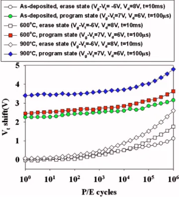
The endurance performances after 106 P / E cycles are
shown in Fig. 5. Again, the rate of memory window narrow-ing increases upon increasnarrow-ing annealnarrow-ing temperature. As we know, the narrowing is mainly coming from charge gain. Because of the use of ultrathin tunnel oxide, there is only very minute amount of trapped charges generated during op-eration in the tunnel oxide.18 Hence, we attribute this to the residual charges along the grain boundaries because these highly localized induced traps are more difficult to remove unless their positions are coincided to overlap with the hot-hole injection. Figure 6 shows the vertical charge migration characteristics with applying Vg-Vt= −12 V at room
tempera-ture 25 °C. Consistent with the former result, the vertical charge migration is exacerbated by increasing annealing tem-perature. With the annealing temperature increases, the more vertical charge loss was found. It can be explained by more leakage path in the grain boundary of crystallized HfO2 in
the high annealing temperature.
B. Disturbances
Figure 7 shows the read disturb induced erase-state threshold voltage instability in a localized HfO2
SONOS-type flash memory cell for three samples. To allow for 2-bit operation, the applied bitline voltage in a reverse-read scheme must be sufficiently large共⬎1.5 V兲 for being able to “read through” the trapped charge in the neighboring bit. Relatively large read bitline voltage may cause unwanted electron injection and then results in a significant threshold voltage shift of the neighboring bit. For our measurement, the gate and drain biases were applied and the source was grounded. The results clearly show that almost no read dis-turbance appears for the low voltage reading operation of
Vg-Vt= 3 V and Vd= 2.5 V in our HfO2flash memory.
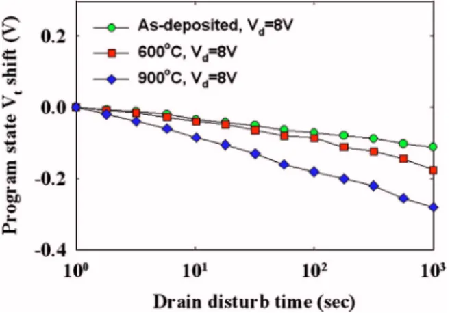
Figure 8 shows the programing drain disturbance of our HfO2SONOS-type flash memories. The same drain voltages
共Vd= 8 V兲 were applied in the programing drain disturbance
measurements at room temperature共T=25 °C兲. Upon the in-creasing annealing temperature, the more drain disturbances were observed. The storage charge leakage path along the grain boundaries induces more drain disturbances for the an-nealed devices. After 1000 s at 25 °C, we have sufficiently drain the disturb margin 共⬍0.3 V兲 for the three annealed samples.
FIG. 5. Endurance characteristics of the HfO2SONOS-type flash memories.
The 900 °C-annealed device shows larger memory window but worse en-durance performance in the same condition.
FIG. 6. Vertical migration characteristics of HfO2SONOS-type flash
memo-ries. Consistent with the former result, the vertical charge migration is ex-acerbated by increasing annealing temperature.
FIG. 7. Read disturbance characteristics of HfO2SONOS-type flash
Figure 9 shows the gate disturb characteristics in the eras-ing state. Gate disturbance may occur dureras-ing programeras-ing for the cells sharing a common wordline while one of the cells is being programed. We measured the gate disturbance with the condition at Vg-Vt= 7 V and Vd= Vs= Vsub= 0 V for the three
annealed samples. With the annealing temperature increases, the more gate disturbances were observed. A large amount of trap generates in the high temperature annealing that induces more gate disturbances for the annealed devices. Only 0.5 V threshold voltage shift has been observed for the 900 °C an-nealed devices after 1000 s stressing. Such good gate disturb characteristic with such thin tunnel oxide can be explained by using the serial capacitor voltage divider model with
small voltage drop at the tunnel oxide. In summary, we have good read, drain, and gate disturbances for the as-deposited, 600 and 900 °C-annealed samples.
IV. CONCLUSION
In this article, we have investigated the effect of post-deposition annealing temperature on the performance of the resultant HfO2 SONOS-type flash memories. Higher
tem-perature treatment can have large memory windows due to the crystallization-induced trap generation, but can lead to poorer retention and endurance performances. Moreover, we found that the HfO2 trapping layer can trap both electrons
and holes. No significant read, drain, and gate disturbances were observed for the three samples. HfO2 SONOS-type
flash memory is considered to be a promising candidate for the flash memory devices application.
ACKNOWLEDGMENT
This project was sponsored by the National Science Council of Taiwan, Republic of China 共Contract No. 942215E009070兲.
1M. H. White, D. A. Adams, and J. Bu, IEEE Circuits Devices Mag. 16,
22共2000兲.
2T. S. Chen, K. H. Wu, H. Chung, and C. H. Kao, IEEE Electron Device
Lett. 25, 205共2002兲.
3T. Sugizaki et al., Proceedings of the IEEE Non-Volatile Semiconductor
Memory Workshop, February 2003共unpublished兲, pp. 60–61.
4T. Baron, B. Pellissier, L. Perniola, F. Mazen, J. M. Hartmann, and G.
Polland, Appl. Phys. Lett. 83, 1444共2003兲.
5R. Ohba, N. Sugiyama, K. Uchida, J. Koga, and A. Toriumi, IEEE Trans.
Electron Devices 49, 1392共2002兲.
6R. Muralidhar et al., Tech. Dig. - Int. Electron Devices Meet. 2003, 601. 7Y. N. Tan, W. K. Chim, W. K. Choi, M. S. Joo, T. H. Ng, and B. J. Cho,
Tech. Dig. - Int. Electron Devices Meet. 2004, 889.
8W. J. Zhu, T.-P. Ma, T. Tamagawa, J. Kim, and Y. Di, IEEE Electron
Device Lett. 23, 97共2002兲.
9G. D. Wilk, R. M. Wallace, and J. M. Anthony, J. Appl. Phys. 89, 5243
共2001兲.
10Y.-H. Lin, C.-H. Chien, C.-T. Lin, C.-Y. Chang, and T.-F. Lei, IEEE
Electron Device Lett. 26, 154共2005兲.
11D. Montanari, J. Van Houdt, D. Wellekens, G. Vanhorebeek, L.
Haspeslagh, L. Deferm, G. Groeseneken, and H. E. Maes, Proceedings of
the IEEE Nonvolatile Memory Technology Conference, June 1996
共un-published兲, pp. 80–83.
12T. Sugizaki et al., Proceedings of the VLSI Symposium Technology Digest
Technical Papers, 2003共unpublished兲, pp. 27–28.
13W. J. Tsai, C. C. Yeh, N. K. Zous, C. C. Liu, S. K. Cho, T. Wang, S. C.
Pan, and C. Y. Lu, IEEE Trans. Electron Devices 51, 434共2004兲.
14C.-C. Yeh IEEE Electron Device Lett. 25, 643共2004兲.
15T. Yamaguchi, H. Satake, and N. Fukushima, Tech. Dig. - Int. Electron
Devices Meet. 2001, 663.
16Y.-W. Chang, T.-C. Lu, S. Pan, and C.-Y. Lu, IEEE Electron Device Lett.
25, 95共2004兲.
17B. De Salvo, G. Ghibaudo, G. Pananakakis, G. Reimbold,F. Mondond, B.
Guillaumot, and P. Candelier, IEEE Trans. Electron Devices 46, 1518 共1999兲.
18E. F. Runnion, S. M. Gladstone, R. S. Scott, Jr., D. J. Dumin, L. Lie, and
J. C. Mitros, IEEE Trans. Electron Devices 44, 993共1997兲. FIG. 8. Drain disturbance characteristics of HfO2SONOS-type flash
memo-ries. After 1000 s at 25 °C, only 0.4 V drain disturb margin is observed for the 900 °C-annealed devices.
FIG. 9. Gate disturbance characteristics of HfO2SONOS-type flash
memo-ries. Only 0.5 V threshold voltage shift has been observed for the 900 °C-annealed devices after Vg-Vt= 7 V and Vs= Vd= Vsub= 0 V, 1000 s stressing.
685 Lin et al.: Annealing temperature effect on the performance of nonvolatile HfO2 685