PERGAMON
Microelectronics Reliability 40 (2000) 1479-1483MICROELECTRONICS RELIABILITY
www.elsevier.com/locate/microrel
Dimensional effects on the reliability of polycrystalline silicon thin-
film transistors
H. W. Zan a, P. S. Shih a, T. C. Chang b'c, and C. Y. Chang a
a Institute of Electronics, National Chao Tung University, 1001 Ta Hsueh Rd, Hsin-Chu, Taiwan b National Nano Device Laboratories, 1001 Ta-Hsueh Rd. Hsin-Chu 300, Taiwan Department of Physics, National Sun Yat-sen University, 70 Lien-hai Rd., Kaohsiung, Taiwan
Abstract
We found that for unpassivated short-channel TFTs, hot carrier stress-induced degradation phenomena are different with various channel geometries. For device with a wide channel width, the threshold voltage is increased while the subthreshold swing is almost unchanged. The stress-induced oxide-trapped charges are responsible for the degradation. For others with narrow channel widths after stress, on the contrary, the subthreshold swing and Im~ . are increased, the trap density is greatly increased and the trap-enhanced kink effect is also observed. This is due to the generation of stress-induced grain boundary traps near the drain side. Additionally, the stress-induced degradations of passivated TFTs with various geometries are identical. The increased defect density dominates the mechanism since the hot-carrier stress tends to break the passivated Si-H bonds. © 2000 Elsevier Science Ltd. All rights reserved.
I. I n t r o d u c t i o n
Polycrystalline silicon thin-film transistors (poly-Si TFTs) have been intensively studied f o r application to high-performance large-area active matrix liquid-crystal display (AMLCD) systems and static random access memory (SRAM). For circuit integration, it is essential to miniaturize the dimension o f poly-Si TFT to meet the requirement of higher circuit density and higher drive current. However, because of the presence of grain boundaries in the poly-Si and the floating-body effect, as the channel length becomes smaller, poly-Si TFTs are known to suffer from severe short-channel effect and behave differently from their counterparts fabricated on single-crystal silicon substrate. Furthermore, stability of poly-Si TFT becomes worse at shorter channel length, which is the key obstacle to circuit integration.
As the grain-boundary trap density is related to the active channel dimension [1, 2, 3], we expect that
~ ~ d e
spacer
Field Oxide
{
Silicon Substrate
1
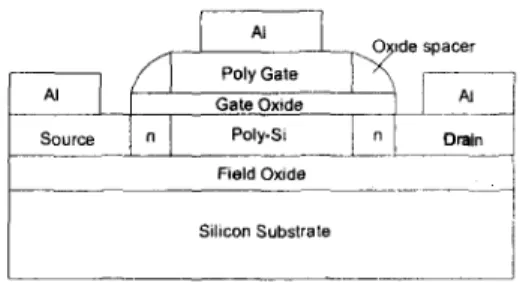
Fig. 1. Polysilicon thin-film transistor structure. the reliability of poly-Si TFTs should also be related to the active channel area. However, until now, little work has done on the influence of channel dimension on the reliability of short-channel poly-Si TFTs. In this paper, we investigate stress effects on short- channel poly-Si TFTs with different geometries and found that channel dimension has a profound influence on reliability.
0026-2714/00/$ - see front matter. © 2000 Elsevier Science Ltd. All rights reserved. PII: S0026-2714(00)00165-7
1480 H. W. Zan et al./ Microelectlvnics Reliabili O, 40 (2000) 1479-1483 70 < zl 60 50 40 gz ~ 30 20 o Z 0 - - s m a l l T F T • " • s h o r t T F T 0 1 2 3 4 5 6 7 Drain Voltage V D ( V )
Fig. 2. The normalized [D-go characteristics o f s m a l l T F T a n d s h o r t T F T .
2. Experiments
The TFTs used in this study are conventional poly-TFTs with top-gate lightly-doped-drain (LDD) structure; the structure is shown in Fig. 1. The channel length of devices is kept at 1.2 # m, while the
channel widths are 20 # m (referred to as s h o r t T F 7
hereafter) and 1.2/z m (referred to as s m a l l TF7 r
hereafter). The process is as follows: First, a 100 nm undoped poly-Si layer was first deposited by low
pressure chemical vapor deposition (LPCVD)
without solid phase crystallization on an oxidized silicon buffer layer and patterned into individual active device islands. Then, a 50-nm TEOS oxide was deposited by LPCVD to serve as the gate insulator. A second poly-Si film was subsequently deposited and patterned to form the gate electrode. Next, lightly doped source/drain regions were formed by phosphorous (with I x l 0 ~3 cm 2 at 55 KeV) implants. A 400-nrn self-aligned sidewall spacer was formed by the deposition o f an TOES oxide layer and subsequent reactive-ion-etching. Afterwards, self- aligned n t source/drain regions were formed by heavy-dose phosphorous (with 5xl 015 cm -2 at 70 KeV) implants. Dopant activation was then performed by rapid thermal annealing (RTA) at 750 °C for 20 seconds. An At film was then deposited and patterned
to form the electrodes, followed by nitrogen
annealing. Finally, 2-hours NH 3 plasma passivation was applied by plasma enhanced chemical vapor deposition (PECVD).
After device fabrication, the typical parameters are extracted from the I-V characteristics of our devices. The threshold voltage V,h is defined as the gate voltage at which IDxL/W = 100 nA for V o = 5V. The trap state density/v; is extracted from the slope of the curve In[Io/(VG-VF~)] versus (Vo-VF~)"- when the
Source
Negative charges at the grain boundaries
I e ~ k avalanche.g e .. . . tee c
~
ctron-hole pairs~ /
Ev
.h recombination
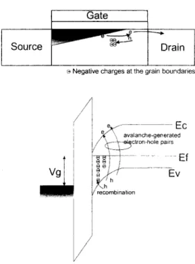
Fig. 3. An illustration to explain the trap-enhanced impact ionization effect.
Table 1 (a) Typical parameters of unpassivated short TF7
Forward Mode Reverse mode
After After Before Before 10000sec 10000sec stress stress stress stress V~h (V) 3.6 • 4.7 3.4 4.7 S.S. (V/dec) 1.24 1.30 1.29 1.32 Imm (pA) 5.7 5.2 5.3 5.1 Nt (Xl0 t2 cm 2) 7.33 7.40 6.81 6.95
Table I (b) Typical parameters of unpassivated small TF7
Forward Mode Reverse mode
After After Before Before 10000sec 10000sec stress stress s t r e s s s t r e s s Vt~ (V) 4.56 5.6 4.8 5.3 S.S. (V/dec) 1.06 1.53 1.09 1.58 Imi n (pA) 0.2 0.35 0.2 0.3 Nt (xl0 Iz cm -~) 5.8 7.5 4.9 8.2
V D is 0. IV. The Imi n and the subthreshold swing S.S. are extracted from the Io-V c characteristics when the VD is 0.1volt. In addition, the stress condition is specified as Vn = V,h + lvolt and VD = Vc + 2.5volt.
tt. W. Zan et al./ Microelectronics Reliability 40 (2000) l 479-1483 1481 le-4 ]e-5 le--6 ,fi le-7 = ,~ Ic-8 le-9
..-7.
T
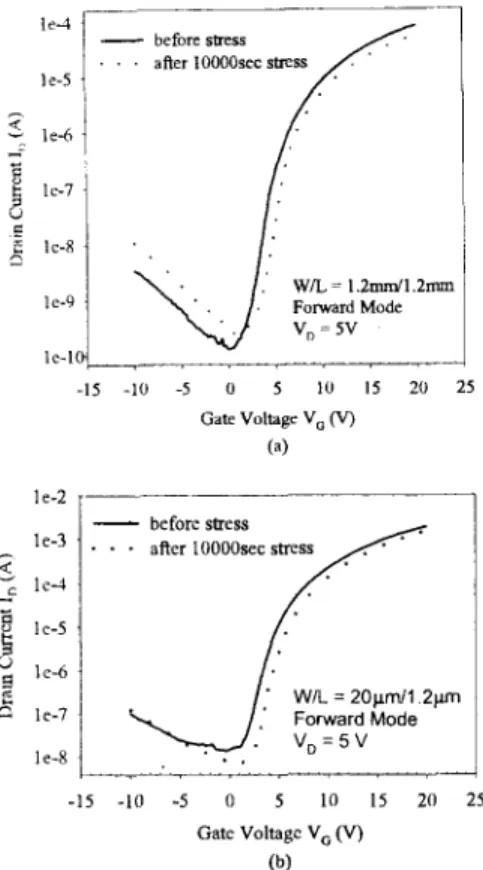
N%" . [ . Forward Mode Vr~ = 5V l e - l ( -15 -10 -5 0 5 10 15 20 25 Gate Voltage V G O r) (a) ] e-2 l e - 3 c le-4 l e-5 1 e-6 le-7 le-8 ' before s t r e s s ~ • . • after 1 0 0 0 0 s e c s t r ~ "?
/." W l L = 2 0 g m / 1 . 2 g m / . ' F o r w a r d M o d e ~ : . , ~ J . . " V o : 5 V -15 -10 -5 0 5 10 15 20 Gate Voltage V 6 (V) (b) 25Fig. 4. The ID-VG characteristics ofunpassivated
(a) small TF7 and (b) short TF7 before and after
gtreg£.
3. Results and Discussions
3. I. Unpassivated short-channel TFTs
The normalized lo-V o characteristics of unpassivated short and small TFTs before stress are shown in Fig. 2, where the normalized I D is define as IDxL/W. It is apparent that they both exhibit kink effects at large drain voltage. Since the channel lengths of the two devices are identical, it is reasonable to expect that the impact ionization rate should be similar. However, for short TFT, the kink effect is more pronounced than small TFT. The explanation is as follows, the short TF7 has a larger N, value than small TF7 since larger active area contains more grain boundaries. Moreover, the kink effect is enhanced with the existence of grain boundary traps [4]. The mechanism is explained by Fig. 3. When impact ionization occurs, the avalanche- generated holes are swept away from the drain
1 2e-4 1 0e-4 8 Oe-5 60e-5 1 4.0e-5 I 20e-5 J [ O.O Unpassivated TFTs WIL = 1 2pm/1 2gm - - before stress • • after 1000gsec stress
1 2 3 4 5 6 7 8 9 tO Drain Voltage Vd ( V ) ( a ) u n p a s s i v a t e d small-dimension TFTs ( V g = 6 , 9 , 1 2 a n d l 5 V ) 1 2e-3 . . . . Unpassivated TFTs 1 0e-3 W/L = 20gm/1 2.tim / [ v - - b e f o r e st . . . . " t / / , " <'~ 8 0e-4 • • after 10000sec s
60e-4 d i~ 40e-4 • . ' 4 20e-4 0O 1 2 3 4 5 6 7 Drain Voltage Vd ( V ) ( b ) unpassivated short-channel TFTs ( V g - 3, 6, 9, 12 a n d 1 5 V )
Fig. 5 The output characteristics of (a) unpassivated
small-dimension TFTs and (b) unpassivated short- channel TFTs before and after 10000-sec hot-carrier stress.
junction and flow toward the source region. Some of the holes will recombine with electrons trapped at the grain boundaries and therefore destroy the electrical equilibrium. Then, many more electrons are injected from the source to the pinch-off region to restore equilibrium. As a result, the larger the trap state density, the more avalanche-generated holes recombine with the negative charge, and the more pronounced the kink effect.
The typical parameters of unpassivated TFTs before and after 10000-sec hot-carrier stress are listed in Table I. For unpassivated short TFT, the threshold voltage is increased after stress while the subthreshold swing S.S. is almost unchanged, impling the generation of oxide trapped electrons after stress. For unpassivated small TF7, on the contrary, the subthreshold swing S.S. is increased after stress, indicating the increase of interface trap density of grain boundary trap density.
1482 14. W.. Zan et al./ Microelectronics Reliability 40 (2000) 1479-1483
Table II (a) Typical parameters ofpassivated short TF7
Forward Mode Reverse mode
After After Before Before 10000sec 10000sec stress stress stress stress Vlh (V) -1.05 -1.32 -1.08 -1.07 S.S. (V/dec) 0.26 0.28 0.28 0.29
Table II (b) Typical parameters ofpassivated small TF7
Forward Mode Reverse mode
After After Before Before 10000sec 10000sec stress stress stress stress Vih (V) . -0.61 -0.52 -0.64 0 S.S. (V/dec) 0.21 0.29 0.20 0.29
The ID-V o characteristics o f unpassivated small TF7 before and after stress are depicted in Fig. 4 (a). It is found that the ratio of the leakage current before
stress IOFF bs to the leakage current after stress IovF a~
remains almost constant independent of increasing gate voltage: This has been reported as the evidence of the increasing grain boundary trap density after stress [5,6]. Consequently, it can be concluded that the stress-induced traps of unpassivated s m a l l TF7
are located in grain boundaries rather than at the silicon/oxide interface. Fig. 4 (b) depicts the ID-Va characteristics o f unpassivated s h o r t TF7 before and after stress. At positive gate voltages, there is a parallel shift o f these characteristics to high absolute gate voltages, showing that the stressing does not create interface states or grain boundary traps which would change the slope o f these result. On the other hand, trapping of electron in the gate oxide is responsible for the increased threshold voltage [5]. Unlike the unpassivated s m a l l TF7, there is strong dependence between the IOFF bs / Iovv ~" ratio and gate voltage for unpassivated short TF7. This indicates that the grain boundary trap generation is not the dominant stress-induced degradation phenomenon.
By comparing the trap density N, o f s m a l l TF7
and s h o r t TFT listed in Table I, it can be found that, after stress, the former is increased greatly than the latter one. It means that under the same hot-carrier stress condition, the stress-induced degradation of
s m a l l T F I seems to be severer than of short TFT.
Similar discrepancy is also observed from the ID-V D characteristics of the two devices shown in Fig. 5 (a) and Fig. 5 (b). The kink effect of short T F T becomes less severe after stress, this is reasonable since the drain current is reduced due to the increased threshold voltage and therefore the kink effect is
5e-4 q
N H 3 Passivated TFTs !
4e-4 W/L = 1 2grnll 2 g m ! ~" / - - before stress . ~ , , , f ~ " ~ , . • " ~" 3 e 4 /
-]
• • after l0000sec stress , • '•
~ ~
2 e - 4
0
0 1 2 3 4 5 6 7 8 9 10 Drain Voltage ( Vd )
(a) passivated small-dimension TFTs
5e-3 4e-3 v o 3 e - 3 2 e - 3 " c3 l e - 3 0 Passivated TFTs J W/L = 20pln11.2pro - - before stress
• • a~ter lO000sec stress
1 2 3 4 5 6
(b) passivated short-channel TFTs
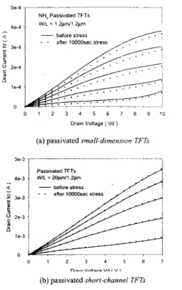
Fig. 6 The output characteristics of (a) passivated
small-dimension TFTs and (b) passivated short-channel TFTs before and after 10000-see hot-carrier stress. (Vg =3,6,9, 12 and 15 V)
suppressed. For s m a l l TFT, on the contrary, the kink effect becomes more pronounced after stress. In spite of the increase of the threshold voltage, the great increase of acceptor-like trap density after stress enhances the kink effect and then dominates the characteristics. The different degradation phenomena of small TFT and s h o r t T F 7 are probably due to the self-heating effect. It is known that the temperature of device will be increased during stress, since the continued high drain current will heat the device. This effect is severer when the channel width is larger [7]. Consequently, the short TF7 should have more pronounced self-heating effect than the small TFT. It has been reported that increasing temperature will suppress the kink effect [8]. The same condition is found from our devices. Therefore, although the stress voltage is kept constant, the stress current of short TFT is reduced with stress time, The stress- induced damage is thus less pronounced.
3.2. P a s s i v a t e d TFTs
The typical parameters of passivated TFTs are listed in Table II, both the threshold voltage V,, and
H. W. Zan et al./ Microelectronics Reliability 40 (2000) 1479-1483 1483 subthreshold swing S.S. increase after stress. This
degradation is due to the increased defect density since the hot-carrier stress tends to break the passivated Si-H bonds. The output characteristics of passivated TFTs are depicted in Fig. 6. By comparing Fig. 5 and Fig. 6, we can find that the kink effect of passivated TFT (with small N~ value) is less severe than it of unpassivated ones (with large N, value). This is consistent with previous discussion that the kink effect is enhanced with increasing Nt value.
4.Conclusion
Under hot-carrier stress, anomalous inconsistent degradation phenomena are found for unpassivated short-channel TFTs with different geometries. Those with narrower channel width tend to suffer more serious stress-induced degradation. Moreover, their kink effect is more pronounced after stress due to the increase of large amount of grain boundary trap density. The trap density of unpassivated short-channel TFT with wide channel width, on the contrary, remains almost the same after stress. The stress-induced degradation is dominated by the generation of oxide-trapped electron. For passivated short-channel TFTs with different geometries, the degradation phenomena are inconsistent. Since the hot-carrier will break the Si-H bonds, the increasing dangling bonds serve as traps
and degrade the device characteristics.
References
[1] N. Yamauchi, J-J. J. Hajjar, and R. Reif. IEEE
Trans. Electro. Devices, vol. 38, no. 1, p. 55,
1991.
[2] N. Yamauchi, J-J. J. Hajjar, R. Reif, K. Nakazawa, and K. Tanaka. IEEE Trans. Electron Devices, vol. 38, no. 8, p. 1967, 1991.
[3] D.N. Yang, Y. K. Fang, K. C. Hwang, K. Y. Lee, K. H. Wu, J. J. Ho, C. Y. Chen, Y. J. Wang, M. S. Liang, J. Y. Lee, and S. G. Wuu. IEEE Electron
Device Lett., vol. 19, no. 11, p. 429, 1998.
[4] P.S. Shih, H. W. Zan, C. Y. Chang, T. C. Chang, and T. Y. Huang. To be published in J p n . ,
Journal Applied Physics.
[5] M. Rodder. IEEE Electron Device Lett., vol. 11, no. 8, pp 346-348, 1990.
[6] J.G. Fossum, a. Ortiz-Conde, H. Sehichijo, and S. Banerjee. IEEE Trans. Electro. Devices, vol. 32, no. 9, p. 1878, 1985.
[7] S. Inoue, H. Ohshima, and T. Shimoda. IEDM, 1997.
[8] M. Koyajagi, H. Kurino, Y. Hashimoto, H. Mori, K. Hata, Y. Hiruma, T. Fujimori, I-Wei Wu, and A. G. Lewis. IEDM, p. 571, 1991.