algorithms have been developed. However, these fast algorithms are often designed to merely reduce arithmetic operations without considering their overall performance in VLSI implementation. In this paper, three criteria are used to compare various block-matching algorithms: 1) silicon area, 2) input/output requirement, and 3) image quality. A basic systolic array architecture is chosen to implement all the selected algorithms. The purpose of this study is to compare these representative BMA’s using the aforementioned criteria. The advantages/disadvantages of these algorithms in terms of their hardware tradeoff are discussed. The methodology and results presented here provide useful guidelines to system designers in selecting a BMA for VLSI implementation. Index Terms— Architecture mapping, block matching, motion estimation, MPEG-2, systolic array.
I. INTRODUCTION
I
N designing a very large scale integration (VLSI) chip, there are tradeoffs among various chip cost and perfor-mance factors particularly from the system design view-point [1]. Since the chip design and layout process is time-consuming and expensive, it is very desirable to be able to predict the overall system performance of a high-level algorithm before its circuit layout is fully deployed. The focus of this paper is to discuss the impact of different block-matching motion estimation (ME) algorithms on VLSI design. Because of the complexity of the entire motion estimation system, decision in choosing one algorithm versus the other algorithms is often empirical and heuristic. For example, the previous motion estimator design often pays attention to only the processor complexity; however, the I/O bandwidth and the on-chip memory size are as important in determining the manufacturing cost.Motion estimation is an essential element in a standard video coder such as H.261, MPEG1, and MPEG2. A straightfor-ward implementation of a block-matching motion estimation algorithm requires a large amount of hardware. Many fast block-matching algorithms have thus been devised to reduce the computational complexity without degrading the
estima-Manuscript received September 30, 1996; revised January 31, 1997. This work was supported in part by the National Science Council of R.O.C. under Grant NSC86-2221-E-009-023.
The authors are with the Department of Electronics Engineering and Center for Telecommunications Research, National Chiao Tung University, Hsinchu, Taiwan 300, R.O.C.
Publisher Item Identifier S 1051-8215(97)05884-9.
search, the conjugate direction search, the alternating pixel-decimation search, and the subsampled motion-field search. Although these algorithms are devised to use fewer arithmetic operations, they may need additional control circuits and data buffers and thus may not lead to lower cost in VLSI manufacturing.
The aforementioned algorithms are chosen not only because of their popularity, but also because they are rather generic and they represent different ways of cutting down the computation. The decimation search reduces the number of data points in each matching calculation, while the other searches try to reduce the number of search points using different techniques (explained in Section II). There are many variations of these algorithms. For example, we could compare the partial results against a properly selected threshold and terminate the search-ing process in the middle to save computation [22]. In addition, there exist many other block-matching algorithms (BMA’s) that we cannot cover here. One structure worth mentioning is the hierarchical algorithm that performs a search first on a loose grid and then on a denser grid [4], [5]. The hierarchical steps can be more than two. In a way, it is a variation of a sequential search (like three-step search). Nevertheless, the analysis described in this paper can be applied to the algorithms not included here.
The hardware implementation of motion estimation algo-rithms can be classified into programmable video signal pro-cessor (VSP) structures and dedicated (special purpose) struc-tures. Programmable VSP structures [7]–[9] allow a higher degree of flexibility; however, they often have a lower through-put rate, higher hardware cost [10], and generally require additional software development effort. Using today’s fab-rication technology, dedicated structures seem to be more economical for mass production. Therefore, we consider only the dedicated structure in this paper.
Typically, a specific motion estimation algorithm is first chosen and then a specific hardware architecture is designed for this chosen algorithm. For example, several hardware implementations are designed for the exhaustive search algo-rithm [11]–[13] and a couple of implementations for the fast algorithms [14], [15]. Also, a few programmable architectures [16]–[18] have been proposed and designed to implement both the exhaustive and some selected fast search algorithms. Usually, these architectures require additional special control
circuit and memory management to set up data paths for different algorithms.
For a specific algorithm such as the sequential (or hierar-chical) algorithm, a well-designed programmable architecture could be rather efficient [18]. However, identifying the optimal VLSI design for every BMA of interest is a very difficult task. One possible approach is collecting all the existing architectures and comparing them. For example, Pirsch et
al. [10] has an excellent summary of the existing ME chips
(but their analysis is focused on the comparison of different
implementations). Even if following this approach, we are not
sure we could claim our choice for Algorithm A is as optimal as that for Algorithm B. Hence, a different approach is taken. We choose a hardware structure as the common ground for comparing all algorithms. Because of its regular layout, high throughput rate, and massive parallel computing capability, systolic array is a very popular and good candidate structure in designing motion estimation chips [11], [19]. Therefore, we also use the systolic array architecture as the basic building block in implementing various block-matching algorithms.
Our goal in this paper is evaluating block matching algo-rithms from mainly the hardware viewpoint. We try to point out that the traditional measure of algorithms, the number of operations, does not match well the VLSI performance. Also, the known fast algorithms have significant VLSI advantages only for large search ranges and large size pictures. We do not intend to find the best algorithm and architecture combination in this study. We compare only algorithms using essentially the same basic hardware structure. Some of the above observations were touched in the past, but we have not seen reports with thorough studies.
The information contained in this paper may serve as a reference or guide to system designers. Given a specific appli-cation (picture size, search range, etc.) a hardware designer can start with a couple of the more promising algorithms and tune the architecture/hardware layout for that specific algorithm. An algorithm (and architecture) designer can also learn from this study what elements are more critical in a BMA for improving VLSI performance and thus designs algorithms accordingly. Furthermore, this work is an attempt to propose a methodology in evaluating algorithms from both VLSI implementation viewpoint and compression performance. A similar study can be applied to the other block matching algorithms and other types of signal processing algorithms. On the other hand, our approach is limited by the varying efficiency of the proposed structure on different algorithms. However, our survey on the existing BMA VLSI structures indicates that this set of implementations should be able to show the distinct advantages and disadvantages of various algorithms in VLSI implementation.
The rest of this paper is organized as follows. Section II describes the block-matching algorithms examined in this paper. Section III discusses the systolic array structures for the evaluated algorithms and their computational complexity. In Section IV, we look into the silicon cost and I/O configu-ration issues for different algorithms in various applications. Section V shows the simulation results of picture quality of the examined algorithms. Section VI briefly summarizes our
TABLE I
MOTIONESTIMATIONPARAMETERS FORCCIR-601ANDCIF PICTURES
work in this paper.
II. BLOCK-MATCHINGMOTIONESTIMATION ALGORITHMS
Block-matching motion estimation is an effective method in reducing the temporal redundancy in video coding and thus is adopted by many video coding standards [2], [5]. The basic operation of a block-matching algorithm is picking up the best candidate image block in the reference image frame by calculating and comparing the matching functions between the current image block and all the candidate blocks inside a confined area in the reference frame. The sizes of image block and confined area (so-called search area) have a strong impact on the performance and the computational complexity of the motion estimation results. A small size block offers a good approximation to the moving object, but it also produces a large amount of redundant motion information data. Small size blocks are easily interfered by random noise. On the other hand, large size blocks may produce a less accurate motion vector since a large block may contain two or more objects moving at different speeds and directions. Block sizes of 8 8 or 16 16 are generally considered adequate from experiments, and thus the international video standards adopt the 16 16 block size, which is used in this study.
To decide an adequate search area is somewhat involved. It depends on both the contents of pictures and the coding system structure. For video-phone applications, small pictures and slow motion are expected, and thus the search range is assumed to be small (around 7 or 15 pels). On the other hand, in MPEG coding, large pictures are expected and the temporal distance between two predictive frames (P-frames) is often greater than a couple of frames [20]. Hence, a large search range (say, 47 pels) is necessary. In addition to block size and search range, picture size and frame rate also have a strong impact on the VLSI cost.
In summary, the important parameters used in the following discussions are: i) picture size (horizontal and vertical), ; ii) picture rate (frames/s), ; iii) block size, ; iv) search range, ; v) external memory bus width, W; and vi) the number of image blocks per second which is derived from
the first three parameters: . The
parameters used in this paper are listed in Table I for CCIR-601 and common intermediate format (CIF) pictures. The former picture format is targeting at digital television (DTV) applications and the latter, video-phone applications.
Another important factor that affects the block-matching hardware complexity is the matching criterion. To reduce
com-SAD AD (1)
SDAD AD (2)
AD
where and are the pel
values in the current block and in the reference (frame) block, respectively, is the pel coordinate relative to the current block location, is the (backward) motion vector, and is the time difference (temporal distance) between the current and the reference frames.
The final motion vector is the one that minimizes the MAD criterion
SAD or SDAD
(3) In general, we need subtractions, absolute operations, and additions to compute one point of SAD . For SDAD, all the aforementioned operations are reduced by a factor determined by the chosen decimation pattern. In the alternate pixel decimation algorithm described in this paper, the reducing factor is four. For the values in the range
of interest such as , can be reasonably
approximated by . The total number of operations needed to compute the MAD criterion is an important attribute of an ME algorithm. In the rest of this section, we briefly describe the operations of the motion estimation algorithms examined in this paper.
A. Exhaustive Search
The most straightforward searching algorithm is the ex-haustive search (full search), which evaluates all the possible displacements (motion vector candidates) inside the search area. In each block time interval, SAD search points and two-term comparisons are calculated to find the best match. In other words, its computational complexity is
on the order of , .
B. Three-Step Search
This popular fast search algorithm is proposed by Koga et
al. [21]. It starts with a step size slightly larger than half of
performed sequentially. In total, there are search
steps and SAD search points for each image
block. It is clear that the number of search steps and points must be an integer and thus denotes the least integer greater than or equal to in the rest of this paper.
C. Modified Log Search
This fast search algorithm is proposed by Kappagantula and Rao [22]. The procedure in this algorithm is similar to that of the three-step search but each search step is broken into two substeps. In the first substep, five search points are evaluated. They consist of the central point of a diamond-shape region and the four search points located one step size away from the central point along the horizontal and vertical directions. If the minimum-SAD position is the central point, the step size is halved and the above process is repeated again. Otherwise, one of the corner points is the minimum point and the second substep is activated. Two additional search points located one step size away from the minimum point are evaluated. These two new search points are located vertically if the first substep minimum point is on the horizontal line. Otherwise, two horizontal search points are used. The minimum among these three search points becomes the center of the new diamond-shape region with a step size equal to half of the previous step size. Then, the next search step starts. The above procedure continues until the step size is smaller than one. The number of SAD calculations in this algorithm varies depending upon the location of the final motion vector. However, we need to consider the worst case situation in VLSI design, and thus
there are SAD operations for each block.
D. Conjugate Direction Search
The conjugate direction search algorithm suggested by Srinivasan and Rao [23] breaks the two-dimensional (2-D) search problem into two one-dimensional (1-D) problems. Assuming that the search starts with the horizontal direction, we first compute the SAD of three candidates located one next to the other. The center candidate is typically the zero motion vector. Then, compare and select the minimum SAD from these three values. If the minimum-SAD position is not the central point, it becomes the new center and the position imme-diately next to it along the minimum-SAD direction is included as the new candidate. The above procedure is repeated until
Fig. 1. Decimated patterns for computing SDAD.
Fig. 2. Alternating patterns of pels in the search region for the APD technique.
the minimum-SAD position is the central point or we hit the search area boundary. In either case, the horizontal direction is completed and we turn to the vertical direction. Starting from the current minimum-SAD point, the same procedure is applied to find the vertical minimum point. The number of operations in this algorithm depends on the location of the final motion vector. In the worst case, there are SAD operations for each block. When the search range ( ) is very large, its computational complexity is on the order of , , larger than that of the three-step search whose computational
complexity is .
E. Alternating Pixel-Decimation (APD) Search
This algorithm is proposed by Liu and Zaccarin [24]. It differs from the previous fast algorithms in that it tries to reduce the calculations involved in each SAD operation but maintains the overall motion estimation performance at a comparable level. The basic concept is to decimate the pels inside a block and compute the differences only on the decimated pels. This algorithm can be explained by using Figs. 1 and 2. Fig. 1 shows a block of 8 8 pels with pels labeled a, b, c, and d in a regular manner. The decimation pattern A is made of all the a pels. Patterns B, C, and D are similarly defined. Fig. 2 shows the pels in (a portion of) the search area. They are labeled 1, 2, 3, and 4. For example, when a 1 pel is a motion vector candidate, pattern A is used as the decimation pattern to pick up the pels in calculating SDAD. Similarly, patterns B, C, and D are the decimation patterns for the candidates located at pels 2, 3, and 4, respectively. For each of these four decimation patterns, the minimum SDAD candidate is retained. Then, for each decimation pattern, the full SAD is computed using all the block pels. The best among them becomes the final motion vector.
Fig. 3. White and shaded blocks in the SAPD technique.
Fig. 4. Block diagram of a general motion estimation chip.
In the above procedure, SDAD operations are needed for one block. In addition, four SAD operations are calculated for the final motion vector selection. If the four SAD operations are neglected for large search ranges, the computa-tional complexity of this algorithm is roughly a quarter of that of the exhaustive search. Hence, its computational complexity is , the same as the exhaustive search.
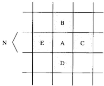
F. Subsampled Motion-Field Search with Alternating Pixel-Decimation Patterns (SAPD)
This algorithm combines both motion field subsampling and the alternating pixel decimation (APD) techniques [24]. There are two stages. At the first stage, we estimate half of the motion vectors using the previous APD technique. The locations of the estimated blocks are indicated by the shaded blocks in Fig. 3. At the second stage, the motion vector of a white block is calculated based on the four vectors of its adjacent shaded blocks. For example, the motion vector assigned to the white block A in Fig. 3 is one of the motion vectors of blocks B, C,
D, or E that gives the smallest SAD value.
In the original formulation [24], block A could be used as a
subblock to increase the motion estimation accuracy. However,
in order to match the MPEG coding structure, block A in this paper has the size of the basic motion estimation unit,
. Thus, for a shaded block, SDAD and
four SAD operations are needed to compute its motion vector. In addition, four SAD operations are needed for each white block. The total computational complexity of this algorithm is approximately reduced by a factor of eight in comparing with
Fig. 5. Block diagram of the 2-D systolic architecture for block-matching.
Fig. 6. Block diagram of the one-column systolic architecture.
the exhaustive search. But its computational complexity is still , the same as the exhaustive search.
III. VLSI IMPLEMENTATION ANDCOMPLEXITYANALYSIS
Several important factors have to be considered in choosing an algorithm for VLSI implementation, for example, i) chip area, ii) I/O bandwidth, and iii) image quality. We will discuss the first two factors in this and the next sections and the third factor in Section V. In implementing block-matching algorithms, the chip area can be approximated by
(4) where is the area used for the computation kernel, is for the on-chip data buffer, and is for the system controller. Because of the massive local connection and parallel data flow in the systolic array structure, a system controller is needed to generate data addresses and flow control signals. Particularly, computing SAD requires specific ordering of data. Therefore, our system controller contains an address generator and a data flow controller.
Due to the very massive data used in computing motion vectors, it becomes impractical for the processor array to
access image data directly from the external memory for it results in a very high bus bandwidth requirement. In addition, the search areas of nearby blocks overlap significantly; hence, an internal reference-data buffer is introduced to relieve some of the external memory access. The block diagram of our motion estimation system with internal buffer is shown in Fig. 4. The memory controller reads in the current and the reference image blocks from external DRAM and stores them in the current-block buffer and the reference-frame buffer, respectively. In this paper, the I/O configuration is referred to as the number of I/O pads and the I/O speed requirement which is constrained by the external memory speed. The external memory bandwidth depends on the size of the internal buffer. This topic will be elaborated in Section IV.
A. Mapping Algorithms to Architectures
Systolic architectures are good candidates for VLSI real-ization of block-matching algorithms with a regular search procedure [19]. A typical systolic array consists of local connections only and thus does not require significant control circuitry overhead. In this paper, a basic systolic array archi-tecture is adopted for estimating the silicon area of various block-matching algorithms. Its general structure is shown in
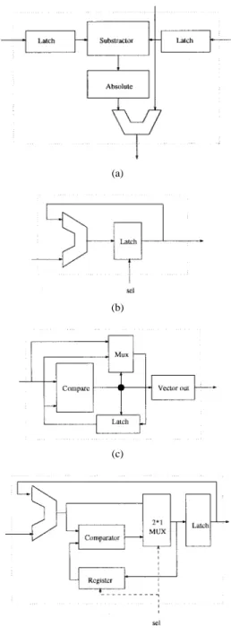
Fig. 5. The processor array (2-D array architecture) consists of 16 16 processor elements (PE’s) or 8 8 PE’s if the APD search technique is in use. If the number of PE’s ( ) is less than or equal to 16, then this system is reduced to one-column architecture as shown in Fig. 6. If the estimated is smaller than the size of a 2-D array but larger than that of a 1-D array (one-column), we then use multiple one-column circuits. In the multiple one-column structures, independent data are processed by several one-column circuits simultaneously. Similarly, multiple 2-D arrays are used when is several times larger than the size of a 2-D array. Four types of computing nodes are used in this structure. Their circuits are shown in Fig. 7. The subtraction, absolute value, and partial sum addition in SAD or SDAD are performed by the PE node. The summation operations are done by the ADD nodes. The CMP nodes compare the matching criteria of the candidates and select the minimum one. The AP node is used to execute the operations of both ADD and CMP when the speed requirement is not critical.
In the 2-D array structure, the current block data, , are first loaded into each PE node. Then, the reference block data, , slide in from the left. The calculation starts from the upper-left corner of the processor array. During the first clock cycle, the node computes the absolute difference between and . The result passes to the PE node below. During the second clock cycle, the node computes
the absolute difference between and and
adds its result to the partial sum propagated from above. In the meanwhile, node computes the absolute difference
between and , and node computes the
absolute difference between and . After 16 clock cycles, the first partial sum,
is completed and placed into the left-most ADD node. In the following clock cycle, this partial sum is passed to the immediate right ADD node and added together with the
second partial sum, . The total
sum (SAD) for the motion vector candidate is completed and propagated to CMP in the following 14 clock cycles. This SAD is compared against the stored SAD resulting from the previous comparison, and then the smaller one is kept in CMP for future comparison. The preceding computation procedure is repeated until all possible candidates are compared and the final motion vector is obtained. The one-column array computation procedure is similar. Some algorithm variations can be implemented with a small addition to the CMP node. For example, the CMP node can be modified to a two-stage structure that compares the calculated SAD with a preselected threshold value at the first stage and then performs the ordinary comparison against the previous matched value. The search process terminates if the calculated SAD is smaller than the threshold. Thus, we realize the “stopping in the middle” feature.
It is clear that an address generator is needed to generate the proper addresses to retrieve data, and then these data have to be distributed properly by a data flow controller (DFC) to the processor array at correct timing. Fig. 8 shows the block diagram of DFC. The output data are broadcasted to
(a)
(b)
(c)
(d)
Fig. 7. Schematic diagrams of PE, ADD, CMP, and AP node elements. (a) block diagram of “PE” node, (b) block diagram of “ADD” node, (c) block diagram of “CMP” node, and (d) block diagram of “AP” node.
the assigned PE nodes during the current clock cycle and then propagated to successive PE nodes in the next clock. The efficiency (EFF) of an array architecture is defined to be the ratio of the active operating time (of all PE’s) to the total operating time (including the idling time for data loading).
The silicon area of the computation kernel used in this architecture can be approximated by
(5)
where , , and are the numbers of PE, ADD,
and CMP nodes, respectively; is the silicon area of one PE, and and are similarly defined. In this architecture, the number of PE’s is decided by clock rate, picture size, and search range. If one-column array is sufficient
Fig. 8. Block diagram of data flow controller.
to process the data in time, it will be chosen to increase the utilization efficiency (EFF) of PE. Otherwise, the 2-D array is forced into use. The PE number, , is also restricted by the maximum system clock. To match the available IC fabrication technology, the maximum clock rate is assumed to be 100 MHz for DTV and 40 MHz for video-phone applications.
Search areas of adjacent blocks overlap quite significantly. This overlapped area data can be stored inside the internal (on-chip) buffer to reduce external memory accesses (bandwidth). Three types of internal buffers for the exhaustive and the APD searches are under evaluation: i) Type A buffer whose size
equals to the search area, pels; ii) Type
B buffer that has the size of one slice of search area; that is, the height of block (or subblock) times the width of search
area, pels; and iii) Type C buffer that
has the size of a block or a subblock, pels. Note that the parameter in the above expressions equals one for SAD calculation and equals two for SDAD (pel decimation technique). For the other search schemes, Type A and C buffers are still meaningful. However, the Type B buffer defined here does not always make sense for sequential searches. Therefore, we may modify the size and the function of the Type B buffer when appropriate. Generally, we assume that the Type B buffer can hold the data needed for processing one search step. This, in fact, in certain cases does not save either computation or bus bandwidth as will be noted.
A picture frame contains picture slices and each slice contains blocks. In order to derive the I/O bandwidth requirement, we first calculate the size of the new data to
be loaded from the external memory down to the on-chip buffer for each block. As shown in Fig. 9(a), the newly loaded data size for the Type A buffer is pels when the next block is on the same picture slice. For processing one picture slice, we need to load the complete buffer at the beginning of a slice; thus, the total external data access is approximately
pels if boundary block cases are neglected. Then, for the entire picture, the total external data access is approximately pels. Similar analysis can be carried over to the cases of Type B and C buffers as shown in Fig. 9(b) and (c). The exact sizes of Type B and C buffers depend on the search algorithms and will be discussed in the next subsection. Either one-port or two-one-port on-chip memory can be used as the internal buffer. The two-port buffer has the advantage of having higher processor utilization efficiency because data read and write can be executed in the same clock cycle. The drawback is it costs more silicon area to implement.
B. Computational Complexity
In this section, we discuss the computational complexity of the motion estimation algorithms described in Section II. There are two stages in loading the reference block data from the off-chip RAM to the systolic array. In the first or the
external stage, data are moved from the off-chip RAM to
the on-chip buffer, and in the second or the internal stage, data are moved from the on-chip buffer to the systolic array
(a)
(b)
(c)
Fig. 9. The block diagrams of overlapped area for three types of buffers. (a) Type A buffer, (b) Type B buffer size, and (c) Type C buffer.
processors. There are two issues involved here. The first issue is the external bus bandwidth requirement so that the external data can meet the demand of the processors, and the second issue is the idling time (stuffing cycles) that the processors are waiting for the data to arrive. Suppose that the first issue has been solved; that is, the external bus bandwidth is wide enough to supply data in time. Under this assumption we investigate the data lag issue.
The total delay time between the go-signal and the time that the processors produce the first output is the external stage delay plus the internal stage delay. This delay time may not introduce processor stuffing cycles if the data can be preloaded into the pipeline and no gap is needed in and between search processes. This is true for the exhaustive search since the data (reference blocks) locations are known ahead of time, and thus the next block data can be preloaded during the current block interval. In the sequential searches, however, the data locations to be used at the next search step are unknown until the current step is completed. In other words, we start loading data to
the systolic array after the previous search step is completed. There is a gap (stuffing cycles) between two search steps. At the beginning of a new search, it takes cycles to fill up the entire systolic array and then two more cycles are needed for the summation and comparison operations. Therefore, our estimate of the stuffing cycles between the completion of the current search step and the first output of the next search step is . There are specific processing structures that can shorten this gap [17]; however, we do not fine-tune our structure for this purpose because our goal is not to design the optimal hardware architecture for any particular algorithm. In reality, a couple of cycles should be added due to the external stage delay, but they are small in number and thus are neglected.
1) Exhaustive Search: The computational kernel of this
algorithm needs to perform at least SAD operations in each block time. If we use only one PE, the clock rate has to be higher than 93.57 GHz for encoding a CCIR-601 4 : 2 : 2 resolution picture with a search range of 47 pels. This is impractical. Typically, the maximum clock speed is upper bounded by the fabricating technology and the I/O limitation. To make our analysis more general, we assume an -MHz clock being employed. The efficiency of systolic architecture for the exhaustive search is nearly 100% because the input data flow is regular and can be arranged in advance. In this case, the number of total PE operations per second is
(6) where is the number of SAD operations for one image block, and is the number of blocks per second (in Table I). Thus, the number of PE nodes required in this structure under the maximum system clock constraint becomes
(7) Here, we assume that multiple copies of systolic structures can be used. The actual value is rounded up to the nearest multiple of 16 (2-D array) or 16 (1-D array). The exact number is determined by the picture size, search range, etc., as to be discussed in the following subsections.
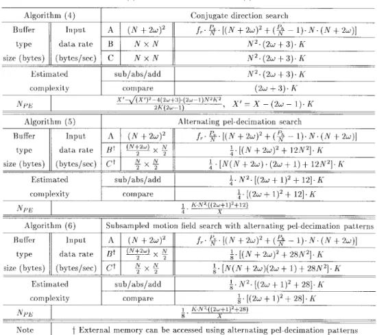
We next consider the on-chip (internal) buffer size and the data input rate. The Type A buffer situation has been discussed in Section III-A. In the case of Type B buffer, it first stores horizontal lines and it then loads one horizontal line when the search moves vertically down one line. In total, additional horizontal lines have to be loaded for the entire search area and each line contains pels. Therefore, the total input data for computing one block is about pels. For the Type C buffer, there are candidate positions on the same line, and in this situation, the new data size for the next position on the same line is pels. Furthermore, the initial data loading for every line is pels. Thus, finishing one line of candidates requires loading pels. Because there are lines of candidates in one search area, the total input
data size for one block is pels. The
input data rate and buffer sizes under different configurations are listed in Table II. They have a strong impact on the silicon size and the I/O bandwidth as will be discussed in Tables IV,
(a)
VI, VIII, and IX. The numbers of “add,” “sub,” “abs,” and “compare” operations in this table are estimated based on the SAD operations needed as described in Section II.
2) Three Step Search: We still use the same basic systolic
structure described in the previous subsection to implement
this algorithm. There are SAD operations
to be performed for each block. Therefore, the total number of required PE operations per second is
(8) If we choose the one-column architecture, pels have to be loaded into the processor array between two search steps, because we do not know which data is to be processed until the completion of the current step. Thus, the efficiency of the one-column structure is approximately
(9)
where and are the time of active operations (in clock cycle) and data preloading (in clock cycle), and is search steps, all in one block interval. Hence
(10) Combining the preceding three equations, we obtain
(11)
where . The value of is smaller
than 256 for CCIR-601 and CIF format pictures. Hence, we can use multiple one-column architectures to save chip area. The data flow controller in this architecture is complicated and needs more chip area than that of exhaustive-search because of the irregular data loading.
Now let us consider the worst case situation of the Type B buffer. In each search step, we need to evaluate eight or nine candidate locations and they are aligned in three rows. If the search step size is fairly large ( ), these data blocks do not overlap. In this case, the Type B buffer that holds the entire search region of a search step does not help in reducing the input data rate. For simplicity, we fix the processing interval for calculating each SAD operation, then we only consider two situations: 1) , Type B buffer has the size of nine
TABLE II (Continued.) (b) IMPLEMENTATIONCOMPLEXITY(2)
(b)
blocks ( in Table II), and 2) , it only needs to hold the search region of the first search step ( in Table II). As the search step gets smaller, the overlapped area among nine candidate blocks becomes larger. Consequently, the required data loading rate decreases. The second search step, not the first step, is the worst case for data loading rate because the data locations of the first step are fixed and thus can be preloaded. Based on the assumption that every search step takes the same amount of computing time, the input data for the second search step is 1) pels for , and
2) pels, otherwise; where denotes
the least integer greater than or equal to . Because there are steps for each block, the data rate is roughly
pels per second for , and
pels per second, otherwise. For the Type C buffer, the worst case is new pels per search
step, and therefore the data rate is pels
per second. The expressions of all the above cases are listed in Table II.
3) Modified Log Search: For this search scheme, we need
SAD operations per block in the worst case. The number of PE operations required in one second is thus
(12) The number of stuffing clocks for data loading in each search step is the same as that of the three-step search
algorithm. Therefore, its efficiency is
(13)
where . Because
, we thus obtain
(14)
where . The column systolic
architecture is adequate for both CIF and CCIR size pictures. Although each search step in the modified log search is broken into two substeps, it would be more convenient and timesaving to allow the buffer to hold the data needed for the entire search step rather than for the substep. Then, the analysis of buffer size and input data rate for this algorithm is similar to that for the three-step search (Table II).
4) Conjugate Direction Search: This algorithm requires SAD operations in a block time interval. When the search range becomes lager, the total amount of computation may be larger than that of the three-step algorithm. This is due to the fact that the number of calculations in this algorithm is on the order and the three-step search is on the
the internal buffer to the processor array. The efficiency of processor array is thus
(15) and the total number of PE operations required in one second is (16)
Again . Therefore, can
be derived from the preceding two equations
(17)
where .
5) Alternating Pixel-Decimation Search: In this technique,
each decimation pattern contains 1/4 of the pels in a block. When the best candidates of all four decimation patterns are found, four matchings are performed to find the overall best one. Therefore, it requires SDAD operations and four SAD operations. Because all the data inside the search region are used, other than the specific address pattern generated for moving data from the internal buffer to the processor array, the internal buffer size and the input data rate for the Type A buffer are identical to those of the exhaustive search. For the Type B and C buffers, because only 1/4 of the pels are used for one decimation pattern, we could complete one pattern search over the entire search area and then continue for the next one. In this case, both the input data rate and the buffer size become 1/4 of those of the exhaustive search as indicated in Table II.
Again the systolic array structure is used in this algorithm. The number of PE operations required in one block interval is roughly 1/4 of the exhaustive search, namely, . The additional four SAD operations would add another PE operations. If we store the best candidate of each search pattern, we may reduce the last four SAD operations down to
PE operations because four SDAD operations (
PE operations) for those candidates have been done already. The total PE operations required per second is thus
(18)
then four SAD operations on each white block. Therefore, on the average, we need
PE operations for every two blocks. In other words, the total PE operations per second is approximately
(20) Then, the efficiency of systolic structure in this algorithm is the same as that of alternating pixel-decimation search. Consequently, the PE number, , is
(21) Because the majority of computations are spent on the APD search, the same buffer sizes in Section III-B-5 for three types of buffers are adopted. However, the data rate is nearly 1/2 of those in the pure APD search because only a few data are needed for the white blocks. These values are listed in Table II.
IV. CHIP AREA AND I/O REQUIREMENT A. Chip Area Estimation
In order to obtain the more exact estimate of chip area, we have done two levels of simulations and analysis. One is the behavioral level and the other is the structure level. At the behavioral level, these algorithms are implemented by C-programs to verify their functionalities. At the structure level, the architectures of the key components in each algorithm are implemented using the Verilog hardware description language (HDL) and then we extract the area information from the Synopsys design tool. In our setup, the Synopsys tool produces an optimized gate-level description using a 0.6- m single-poly double-metal (SPDM) standard cell library.
As discussed earlier, the search range depends on both the coding system structure and the applications (picture size and content). In a typical MPEG-2 encoder, the search range can
be empirically decided by [25], where
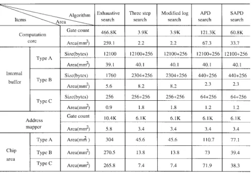
represents the distance between the target and the reference pictures. Hence, in the first application for encoding CCIR-601 pictures, the search range is chosen to be 47 for encoding P-pictures (distance ). The chip area estimates for the computation kernels in various cases are listed in Table III. In this table, the meaning of no. of PE operations, no. of PE
TABLE III
ESTIMATEDAREA OFCOMPUTATIONCORE FORCCIR-601 PICTURES
TABLE IV
ESTIMATED AREA OF THEENTIRECHIP FORCCIR-601 PICTURES
nodes, and Architecture Efficiency are defined in Section
III-B as , , and . The item Chosen comes
from rounding the number up to the nearest integer of multiples of 16 (or 8) that can fit into the chosen array architecture. The speed requirement of PE node is obtained by dividing the number of PE operations ( ) by the Chosen PE entry. The areas of PE, ADD, and CMP are provided by the Synopsys tool under the clock rate given in the Speed entry.
In this design, we choose a two-port internal buffer to increase the PE utilization efficiency. The buffer size and access time requirement are determined by the chosen system architecture. However, the two-port memory module is not included in our ASIC library. Hence, an area estimation model of two-port memory proposed by Chang [26] is adopted to generate the entries in Table IV. When the chosen is
larger than the block size, the 2-D systolic structure (Fig. 5) is then used. In the 2-D structure, the current block data can be preloaded into each PE; therefore, the current block buffer can be eliminated. It cannot be eliminated in the 1-D structure. But in either case, we always need the reference block buffer (the Type A, B, or C buffer), which is often much bigger.
A list of areas of the critical elements in various block-matching algorithms is shown in Table IV. At the end of this table, the total chip area, specified by (4), is the combination of the computation kernel, the internal buffer, and the data mapper. It is interesting to see that the area of the internal buffer may be larger than that of the computation core. For easy comparison, the total area using different types of buffers are listed. The systolic architecture may be an inadequate choice for the conjugate direction search
TABLE VI
ESTIMATED AREA OF THEENTIRE CHIP FORCIF PICTURES WITHSEARCHRANGE= 7 PELS
algorithm because its pipeline efficiency is lower than 50%. From Table IV, we find that the chip area of the full-search algorithm is approximately ten times larger than that of the other algorithms for CCIR 601 pictures. If the chip area is our only concern, the three-step search and modified-log search have about the same chip area and seem to be the preferred choices. Although Type B or C buffers require smaller chip area, they demand a higher I/O bandwidth (to be discussed in the next section), we may be forced to chose the Type A buffer configuration, which has the advantages of a smaller I/O bandwidth and a simpler address generator.
In the second design, we estimate chip area for a smaller picture (CIF format) and slow motion application. Since only I-picture and P-picture are used in low-resolution video coder (H.261), two search ranges are tested: 7 and 15. Tables V and VII show the areas of the key elements in the computational
kernel for CIF pictures at two search ranges. Because one PE is sufficient for fast search algorithms, their efficiency is 100%. The estimated chip areas are listed in Tables VI and VIII. Because the I/O bandwidth limitation is not severe in this case, Type B or C buffers could be reasonable choices in this case. We find that the conjugate direction search has a somewhat lower chip area. However, the conjugate direction search often has the lowest image quality (Section V). Therefore, the other fast searches are also good candidates. For a search range of 7 pels, the chip areas for all algorithms are quite close.
From the above results, we find that the buffer portion is the dominant factor in chip area for the sequential searches particularly for small size pictures. In contrast, the area of the computation core dominates the entire chip area for the exhaustive type of searches (including APD and SAPD) par-ticularly for large size pictures. Therefore, if the picture size
TABLE VII
ESTIMATEDAREA OFCOMPUTATIONCORE FORCIF PICTURES WITHSEARCHRANGE= 15 PELS
TABLE VIII
ESTIMATED AREA OF THEENTIRE CHIP FORCIF PICTURES WITHSEARCHRANGE= 15 PELS
and/or search range are huge, the three-step search and the modified-log search have about the same chip area and are the preferred choices. We like to emphasize again that our estimates of chip area are rough and the architecture used here is not tuned to a particular algorithm, although it may happen to be a better implementation of certain algorithms. Therefore, the analysis here provides only the global picture and overall tendency rather than the accurate and final specifications. For the same reason, we did not perform the same analysis on many different size pictures and other search ranges since we can already see the advantages and disadvantages of these search algorithms through some representative cases.
B. Chip I/O Configurations
The number of I/O pads is one major factor in chip fabrication cost. There are roughly three types of I/O pins:
is the bus width connected to the external memory, and are the pads for control signal and power supply. Although the values of and may depend on the system architecture, there are no simple rules to estimate them. Often, they do not vary very much. (It was reported [11] that they are around 28.) We now only look into the bandwidth requirement due to input data. There are two approaches in calculating the I/O bandwidth requirement. We could assume a minimum external memory access time (decided by the available DRAM, say) and then calculate the minimum bus width, . Or, we first assume the value, and then calculate the maximum allowable memory access time. In Table IX, the latter approach is taken and we assume that equals to . The necessary input data speeds in various cases are calculated based upon the discussions in Section III-B. For example, for the CCIR picture application, if the Type B buffer
Fig. 10. PSNR performance of motion estimation algorithms on the CCIR
Football sequence.
is chosen and the external memory bus width is 64 ( ), this table tells us that the external memory access time must be less than ns for the full (exhaustive) search. A larger access time implies an easier situation that either we could find a slower speed DRAM to meet our requirement or we could reduce the memory bus width (smaller ). As one may expect, the Type A buffer is preferred at the cost of a larger internal buffer. Practically, if the ordinary low cost DRAM is used as the external memory with an access time of 60 ns and the bus width ( ) is around 60 too, then the entries less than in Table IX are not acceptable. That is, the Type A buffer is nearly the only choice for CCIR pictures with a search range of 47. On the other hand, if is greater than 20, all three types of buffers can be used for CIF pictures with a search range of 15 or less. One additional remark is that in the case that the motion estimator is a part of a video encoder chip, it may not own completely the I/O pins, but its bandwidth requirements usually have a strong impact on the entire chip—the motion estimator is often the most demanding unit on data access.
Fig. 11. PSNR performance of motion estimation algorithms for the CCIR
Bus sequence.
Fig. 12. PSNR performance of motion estimation algorithms on the CIF
Table Tennis sequence, search range = 7 pels.
V. PICTURE QUALITY
Since different block-matching algorithms are used, their image qualities are not identical. Although peak signal-to-noise ratio (PSNR) may not be a good measure for the subjective image quality, it can still be used as an indicator for quality comparison. The PSNR is defined as the ratio of the peak signal power (255 ) to the mean square motion estimation errors. Several sequences have been tested. Limited by space, only three of them are reported here. Another measure of the effectiveness of a motion estimation algorithm is the number of bits necessary to transmit the estimation errors. For simplicity, we calculate only the first-order entropy [3].
Figs. 10 and 11 show the motion estimation errors of the CCIR 601 image sequences Football and Bus. Only the processed picture frames are displayed in the figures. In this simulation, the search range is 47 for P-pictures and 15 for B-pictures. Figs. 12 and 13 show the results of two 10-frames/s
Fig. 13. PSNR performance of motion estimation algorithms on the CIF
Miss American sequence, search range = 15 pels.
CIF image sequences Table Tennis and Miss America with a search range of 7 and 15, respectively. Except for the first frame, the rest are all P-pictures. It is clear that the full search algorithm outperforms all the other algorithms. The three-step search and the modified log search are lower by roughly 1 dB in PSNR. Their PSNR values in all four sequences are very close to each other. Similar trends are shown in the entropy results, Figs. 14 and 15. In general, the pixel-decimation technique (APD) has a better performance on slowly moving pictures (such as Table Tennis and Bus) but has a poorer performance on fast moving pictures (such as
Football). The conjugate direction search has a PSNR quite
a bit lower than that of the other search algorithms. Hence, unless there is a significant advantage in hardware cost, the conjugate direction search is not preferred from the image quality viewpoint. One may note that in order to match the video coding standards in which the block is 16 16, the so-called subblock in the original SAPD [24] is now 16 16 rather than 8 8. The larger subblock size slightly reduces its performance. If the picture quality is our major concern, the exhaustive search is the best choice. However, for large size pictures and/or large search ranges, the three-step and the modified-log searches have a much lower hardware cost and only a somewhat lower picture quality.
VI. CONCLUSIONS
The purpose of this study is not to propose a VLSI ar-chitecture for implementing a specific BMA, but to evaluate various block-matching algorithms from the viewpoints of both VLSI design and compression efficiency. A procedure is suggested to assist VLSI designers to choose a good block-matching algorithm adequate for their particular applications. Our assessment on BMA in this paper is based on silicon area, I/O requirement, and image quality. A universal systolic arrays structure is used to realize all the BMA candidates. A distinct feature in our study is to look into the effect of different sizes of the on-chip memory. Although we did not
Fig. 14. Entropy performance of motion estimation algorithms on the CCIR
Football sequence.
Fig. 15. Entropy performance of motion estimation algorithms on the CIF
Miss American sequence, search range = 15 pels.
complete the layout of each realization, the key elements in the hardware have been implemented using Verilog language and their silicon areas are extracted with the help of Synopsys tool based on a 0.6- m SPDM standard cell library.
Examples of applications at CIF and CCIR-601 picture resolutions are examined. In summary, we found that the relative performance in chip area and I/O bandwidth between various algorithms is strongly picture size- and search range-dependent. For small pictures (CIF, for example) and slow mo-tion (small search range), all the BMA’s under consideramo-tion are on a par. However, for larger picture sizes (CCIR-601) and fast motion, certain fast search algorithms have the advantage of a significantly smaller chip area. For a specific algorithm, one may tune the hardware structure to achieve an even more economical design. Nevertheless, we have conducted a comprehensive study on estimating the complexity of various motion estimation algorithms, their chip area, data bandwidth,
J. W. Woods, Eds. San Diego, CA: Academic, 1995.
[6] K. R. Rao and J. J. Hwang, Techniques and Standards for Image, Video,
and Audio Coding. Upper Saddle River, NJ: Prentice Hall, 1996. [7] T. Akari et al., “Video DSP architecture for MPEG2 codec,” in Proc.
ICASSP’94. IEEE Press, 1994, vol. 2, pp. 417–420.
[8] T. Inoue et al., “Programmable vision processor/control for flexible implementation of current and future image compression standards,”
IEEE Micro, vol. 12, pp. 33–39, Oct. 1992.
[9] J. Goodenough et al., “A general purpose, single chip video signal processing (VSP) architecture for image processing, coding and com-puter vision,” in IEE Colloquium on Parallel Architectures for Image
Processing, 1994, pp. 1/1–1/4.
[10] P. Pirsch, N. Demassieux, and W. Gehrke, “VLSI architectures for video compression—A survey,” Proc. IEEE, vol. 83, no. 2, pp. 220–246, Feb. 1995.
[11] K. M. Yang, M. T. Sun, and L. Wu, “A family of VLSI design for the motion compensation block-matching algorithm,” IEEE Trans. Circuits
Syst., vol. 36, pp. 269–277, Oct. 1989.
[12] L. De Vos and M. Stegherr, “Parameterizable VLSI architectures for the full-search block-matching algorithm,” IEEE Trans. Circuits Syst., vol. 36, pp. 1309–1316, Oct. 1989.
[13] S. H. Nam, J. S. Beak, and M. K. Lee, “Flexible VLSI architecture of full search motion estimation for video applications,” IEEE Trans.
Consumer Electron., vol. 40, May 1994.
[14] A. Costa et al., “A VLSI architecture for hierarchical motion estima-tion,” IEEE Trans. Consumer Electron., vol. 41, May 1995.
[15] H.-K. Jung et al., “A VLSI architecture for the alternative subsampling-based block matching algorithm,” IEEE Trans. Consumer Electron., vol. 41, pp. 231–238, May. 1995.
[16] L. De Vos and M. Sch¨obinger, “Efficient architecture of a programmable block matching processor,” in Intel. Conf. Application-Specific Array
Processors, Oct. 1993, pp. 560–571.
[17] Y. S. Jehng, L. G. Chen, and T. D. Chiuh, “An efficient and simple VLSI architecture for motion estimation algorithms,” IEEE Trans. Signal
Processing, vol. 41, pp. 889–899, Feb. 1993.
[18] H.-D. Lin et al., “A programmable motion estimator for a class of hierarchical algorithms,” in VLSI Signal Processing VIII. New York: IEEE Press, 1995.
[19] T. Komarek and P. Pirsch, “Array architectures for block matching algorithms,” IEEE Trans. Circuits Syst., vol. 36, pp. 269–277, Oct. 1989. [20] R. Aravind et al., “Image and video standards,” in Handbook of Visual
Communications, H.-M. Hang and J. W. Woods, Eds. San Diego, CA: Academic, 1995.
Sheu-Chih Cheng received the B.S. degree in elec-tronics engineering from National Taiwan Indus-trial Technology, Taipei, Taiwan, in 1989 and the M.S. degree from National Chiao Tung University, Hsinchu, Taiwan, in 1991. He is currently working toward the Ph.D. degree in electronics engineering at National Chiao Tung University.
His research interests are video coding and VLSI design for signal processing.
Hsueh-Ming Hang (S79–M’80–SM’91) received the B.S. and M.S. degrees from National Chiao Tung University, Hsinchu, Taiwan, in 1978 and 1980, respectively, and the Ph.D. degree in electrical engineering from Rensselaer Polytechnic Institute, Troy, NY, in 1984.
From 1984 to 1991, he was with AT&T Bell Laboratories, Holmdel, NJ. He joined the Electron-ics Engineering Department of National Chiao Tung University, Hsinchu, Taiwan, in December 1991.
Dr. Hang was a Conference Co-Chair of the Symposium on Visual Communications and Image Processing (VCIP), 1993, and the Program Chair of the same conference in 1995. He guest co-edited two Optical Engineering special issues on Visual Communications and Image Processing in July 1991 and July 1993. He was an Associate Editor of IEEE TRANSACTIONS ON IMAGE PROCESSING from 1992 to 1994 and a co-editor of the book Handbook of Visual Communications (Academic Press, 1995). He is currently an Associate Editor of IEEE TRANSACTIONS ONCIRCUITS AND SYSTEMS FOR VIDEO TECHNOLOGYand an Editor of Journal of Visual
Communication and Image Representation (Academic Press). He is a member