0257-8972/04/$ - see front matter䊚 2003 Elsevier B.V. All rights reserved. doi:10.1016/j.surfcoat.2003.06.016
Effects of the Sb Te crystallization-induced layer on crystallization
2 3behaviors and properties of phase change optical disk
Wei Hsiang Wang, Li Chun Chung, Cheng Tzu Kuo*
Department of Materials Science and Engineering, National Chiao Tung University, 1001 Ta-Hsueh Road, Hsinchu 300, ROC Taiwan
Abstract
The conventional phase-change optical disk is generally fabricated by the sputtering process, which has a drawback of requiring an initialization process to change the as-deposited recording layer in the disk fromamorphous to crystalline phases before the disk can be used for reading or writing. In order to develop an initialization-free process, the Sb Te alloy was used as an2 3 additional layer below or above the recording Ge Sb Te layer to study its effect on crystallization behaviors of the recording2 2 5 layer. The layer structures were deposited on substrates of Si wafer, Cu-mesh to examine crystal structure(XRD),
amorphous-to-crystal transformation (DSC) and microstructure (TEM). The complete disk specimens were prepared on PC board to measure
their dynamic properties, such as reflectivity, jitter and modulation (dynamic tester); and to examine the effects of laser pulse
duration time, position and thickness of Sb Te layer on static reflectivity of the disk2 3 (static tester), where Avrami coefficient ‘q’
in J-M-A rate equation can be derived. The results show that effect of Sb Te layer is essentially to induce crystallization of2 3 Ge Sb Te recording layer from2 2 5 (110) plane of Sb Te crystals. This is due to the fact that the crystallization temperature of2 3 Sb Te crystal is 85 8C below that of Ge Sb Te crystal, in addition to a lower lattice mismatch between two crystals. The is in2 3 2 2 5 agreement with the J-M-A kinetic analyses that the rate controlling step for amorphous-crystal transformation in disk specimens with Sb Te layer over 15-nmthickness is mainly governed by nucleation with2 3 qs2.53–2.79)2.5 in J-M-A equation. Regarding
the effects of Sb Te layer on disk properties, the results show that under the 10 nmGe Sb Te layer thickness, the Sb Te -2 3 2 2 5 2 3 assisted disks with lower Sb Te layer thickness between 13 and 20 nm show the best combination of reflectivity and modulation.2 3 The most important advantage of this process is that the Sb Te -assisted disks require no initialization process, because the as-2 3 deposited disks can be directly written and erased.
䊚 2003 Elsevier B.V. All rights reserved.
Keywords: Phase-change optical disk; Initialization-free; Digital versatile disk; Ge Sb Te recording layer2 2 5
1. Introduction
Phase-change rewritable optical disks were widely applied in the data storage in the past few years. Phase-change disk (PD) is the first commercial product in the world and the rewritable compact disk (CD-RW) came to market in 1996 and became the main product of phase-change media until now. As the demand for storage capacity increased, the digital versatile disk-rewritable (DVD-rewritable) media were widely
devel-oped and commercialized within the past 5 years. The existing products have many kinds of formats including DVD-RAM, DVD-RW and DVDqRW. The recording material and layer design may be different between all *Corresponding author. Tel.: 5731-949; fax: q886-3-5721-065.
E-mail address: [email protected](C.T. Kuo).
kinds of rewritable DVD products but the process of manufacturing is almost the same. The conventional phase-change optical disc is generally fabricated by the sputtering process, which has a drawback of requiring an initialization process to change the as-deposited recording layer in the disk fromamorphous to crystalline phases. In order to minimize the cost, many researches have been carried out to skip this initialization process
w1–3x. Miao et al. w1,2x proposed that Sb Te filmcould2 3
be used as an additional layer to enhance the crystalli-zation of recording layer during low temperature sput-tering process, which is called ‘Initialization-free’ process. Tominaga et al. w3x reported that the additional Sb layer could also enhance the crystallization of AgVInSbTe recording material in the disk.
Although effect of enhanced crystallization with addi-tional Sb Te layer was reported in the literature, the2 3
satisfac-Table 1
Disk sample designations and their layer structures, including their thickness, reflectivity and modulation
Layer ZnS–SiOa 2 Sb Te2 3b Ge Sb Te2 2 5c Sb Te2 3d ZnS–SiO2e Al–Tif Rg Mh Sample (nm) (nm) (nm) (nm) (nm) (nm) (%) (%) design DK1 95 7 10 3 15 100 9.45 24 DK2 95 7 10 7 15 100 10.12 43 DK3 95 10 10 10 15 100 16.29 46 DK4 95 15 10 15 15 100 19.24 18 DK5 95 0 10 10 15 100 i i DK6 95 0 10 15 15 100 i i DK7 95 5 10 0 15 100 9.4 24 DK8 95 10 10 0 15 100 10.41 42 DK9 95 15 10 0 15 100 14.41 45 DK10 95 20 10 0 15 100 17.21 43 DK11 95 25 10 0 15 100 15.0 i
Lower dielectric layer. a Lower Sb Te layer. b 2 3 Recording layer. c
Upper nucleation assisting layer. d
Upper dielectric layer. e Reflective layer. f Rsreflectivity. g msmodulations(I yI )yI =100%. h
14max l4min 14max They are too low to be measured. i
Fig. 1. Layer structure of disk samples.
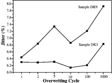
Fig. 2. Overwriting cycle dependence of jitter for samples DK3 and DK9.
torily. Therefore, it has not been accepted commercially. In this study, the effect of additional Sb Te layer on2 3
crystallization behaviors of Ge Sb Te2 2 5 layer and its kinetic mechanisms were examined. An initialization-free process for commercial applications will be proposed.
2. Experimental
The disk samples with various layer structures were prepared on the 2.6 GB DVD-RAM polycarbonate substrates of 0.6-mm thickness by a sputtering machine with six DC magnetron and RF sputtering guns(Helix). After layer structure depositions, a bonding process is carried out to cove with another plane polycarbonate substrate to become a complete disk sample. The dep-osition conditions are shown in Table 1, and the layer structures are depicted in Fig. 1. In these samples, the
Sb Te additional layer was deposited on one side or2 3
both sides of the Ge Sb Te recording layer with various2 2 5
thickness to examine their effects on disk reflectivity and modulation. A dynamic tester (Pulstec DDU-1000)
was used to determine the reflectivity, modulation and jitter of the disk samples. Where the jitter as a function of overwriting cycle for Samples DK3 and DK9 is shown in Fig. 2.
The three different samples on Si wafer were prepared for XRD examination to determine the degree of amor-phous-crystal transformation after sputtering or sputter-ingqannealing processes: (1) the as-deposited
Fig. 3. XRD patterns of the as-deposited Sb Te2 3ySi and Sb Te2 3yGe Sb Te ySb Te ySi stacks, the annealed Ge Sb Te ySi2 2 5 2 3 2 2 5 stack.
Fig. 4. TEM micrograph of Ge Sb Te2 2 5ySb Te stack on Cu-mesh.2 3 Sb Te2 3(40 nm)ySi and (2) Sb Te (7 nm)yGe Sb Te2 3 2 2 5
(10 nm)ySb Te2 3 (15 nm)ySi, (3) the annealed
Ge Sb Te2 2 5 (50 nm)ySi at 200 8C for 30 min.
The reflectivity vs. laser pulse duration time for disk samples DK7–DK9 was measured by a two-laser static tester (Tueoptics) to study J-M-A kinetic equation for
amorphous-crystal transformation. Here, the 659 and 633 nmlasers were used to write and erase mark and to monitor the reflectivity change of mark, respectively. The reflectivity of completely amorphous state (R ) ofa
the disk could be obtained by using the writing power of 11 mW for 70 ns duration. The reflectivity (R ) fort
different laser pulse duration time was determined by using the erasing power of 6 mW. When the reflectivity approaches a constant value as the pulse time increases, the value is called the reflectivity (R ) of completec
crystalline state.
The sample for TEM examination was prepared by sputtering the multi-layer Ge Sb Te2 2 5 (10 nm)ySb Te2 3
(10 nm) on Cu-mesh to study the interface structure of
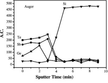
the layers. The sample for Auger analysis was prepared by sputtering the Sb Te2 3 (10 nm)yGe Sb Te (10 nm)y2 2 5
Sb Te2 3 (15 nm) on Si wafer to examine the possible
diffusion among three layers and Si wafer.
3. Results and discussion
3.1. Effect of the SbTe layer position and thickness
The reflectivity is an index to indicate the degree of amorphous–crystalline transformation of the Ge Sb Te2 2 5
recording layer in the disk. The modulation is defined in Table 1, where I14max and I14min represent the maxi-mum and minimaxi-mum intensities of the disk with 14T laser pulse duration time, respectively (Ts34.2 ns). It
is an index to indicate the ability of signal to be detected. Table 1 shows that the upper Sb Te2 3 layer has no significant effect on reflectivity of the as-deposited disk samples, where the upper layer is the layer deposited after deposition of Ge Sb Te recording layer. In con-2 2 5
trast, dependence of the reflectivity and modulation of the disk on thickness of lower Sb Te layer is shown in2 3
Fig. 6. It indicates that the maximum values of reflec-tivity and modulation of the disks are around a thickness of 20 nmand 13 nm, respectively. In other words, under the 10 nmGe Sb Te layer thickness, the Sb Te -assisted2 2 5 2 3
disk with lower Sb Te layer thickness between 13 and2 3
20 nmshows the best combination of reflectivity and modulation. When the thickness of lower Sb Te layer2 3
is too low, the layer will become the isolated islands instead of continuous film. If the thickness is too thick, the transmittance of the films will decay drastically and the modulation of signal will become undetectable. Where the lower Sb Te2 3 layer is deposited before Ge Sb Te recording layer. In other words, the lower2 2 5
Sb Te2 3 layer can enhance the crystallization of the Ge Sb Te recording layer during its deposition. This is2 2 5
due to the fact that the crystallization temperature of the Sb Te alloy is 85 8C below that of Ge Sb Te alloy.2 3 2 2 5
Where the crystallization temperature was analyzed by differential scanning calorimetry(DSC). In other words, the lower Sb Te layer can be much easier to become2 3
crystalline state after deposition, and then acts as the nucleation site to enhance crystallization of the Ge Sb Te layer. It is known that the lattice mismatch2 2 5
between the Sb Te and Ge Sb Te crystals is low, which2 3 2 2 5
favors nucleation of crystal on the matching crystallo-graphic plane. On the contrary, when the Ge Sb Te2 2 5
layer is solidified after its deposition, the additional upper Sb Te layer will have no significant effect on2 3
crystallization of the Ge Sb Te recording layer. There-2 2 5
fore, it is concluded that the position and thickness of the additional Sb Te layer are two important factors to2 3
Fig. 5. Auger depth profile of the as-deposited Sb Te2 3yGe Sb Te ySb Te ySi stack.2 2 5 2 3
Fig. 6. Thickness dependence of reflectivity and modulation of lower Sb Te nucleation assisting layer2 3 (samples DK7–DK11).
3.2. XRD analysis
The XRD patterns are shown in Fig. 3 for the as-deposited Sb Te2 3 (40 nm)ySi and Sb Te (7 nm)y2 3
Ge Sb Te2 2 5 (10 nm)ySb Te (15 nm)ySi, the annealed2 3
Ge Sb Te2 2 5 (50 nm)ySi stacks, respectively. It indicates
same diffraction angle near 42.4 degree for the annealed Ge Sb Te2 2 5ySi and as-deposited Sb Te ySi stacks. The2 3
same but lower intensity diffraction peak of 42.48 can also be detected for the as-deposited Sb Te2 3yGe Sb Te y2 2 5
Sb Te2 3ySi stack. This signifies that the Ge Sb Te layer2 2 5
can partly become a crystalline state after deposition due to the presence of lower Sb Te stack. The lattice2 3
matching plane between Sb Te and Ge Sb Te crystals2 3 2 2 5
must be (110) plane of the Sb Te crystal. In other2 3
words, the self-crystallization of Ge Sb Te layer during2 2 5
deposition is possible by applying an optimum thickness of the lower Sb Te layer.2 3
3.3. TEM analysis
In order to examine the coherency of the interface between the Ge Sb Te and Sb Te crystal, the multi-2 2 5 2 3
layer Ge Sb Te2 2 5 (10 nm)ySb Te (10 nm) films were2 3
prepared on Cu-mesh by sputtering. The corresponding TEM micrograph of the as-deposited films is shown in Fig. 4. The surface is mainly the Ge Sb Te phase. It is2 2 5
obvious that there are some Moire fringes at certain positions. It may signify a slight mismatch between two layers. This is in agreement with the XRD results.
3.4. Auger analysis
The as-deposited Sb Te2 3 (10 nm)yGe Sb Te (102 2 5
nm)ySb Te (15 nm) stacks on Si wafer were examined2 3
by Auger depth profile analysis, as depicted in Fig. 5. It is obvious that three distinct layers can be observed.
There is no significant inter-diffusion between layers after sputtering deposition, though the layer thicknesses are in nanometer ranges.
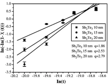
3.5. J-M-A kinetic analysis
By assuming a linear relation between the reflectance and the crystallized fraction w4x, it leads to Eq. (1):
x(t)s(R yR )y(R yR )t a c a (1)
where x(t) is the crystallized fraction of specimen
collected by static tester, R and R denote the reflec-c a
tance of completely crystalline and completely amor-phous films, respectively, and R is the reflectance oft
the sample at laser pulse time ‘t’. According to the
J-M-A model, the crystallized fraction, x(t), can be
expressed by:
q
w x
x(t)s1yexp y(kt) (2)
where q is called Avrami coefficient w5,6x, and k is
Boltzmann’s constant. By plotting lnwyln(1yx(t))x against ln(t), it results in a straight line with slope q.
Fig. 7 shows dependence of q value on thickness of
lower Sb Te layer in the disk. It indicates that2 3 q value
increases as the thickness increases. Generally speaking,
q value determines the rate controlling mechanism of
crystallization. When q value is less than 1.5, the
crystallization process is dominated by grain growth.
When q value lies between 1.5 and 2.5, the rate
controlling processes are both of grain growth and nucleation. As the q value is greater than 2.5, the
nucleation is the dominant rate controlling process w5,6x. In other words, it shows that the process is governed by nucleation as the thickness of lower Sb Te layer )152 3
nm (qs2.53–2.79). This is in agreement with the previous conclusion that the lower Sb Te layer with2 3
Fig. 7. The lnwyln(1yx(t))x versus ln(t) curves at three different thicknesses of the lower Sb Te layer, which are used to derive Avrami2 3 coefficient (q) (slope of the curves) for samples DK8, DK9 and DK10.
optimum thickness can effectively act as nucleation sites to enhance crystallization of Ge Sb Te layer.2 2 5
3.6. Jitter analysis
Jitter is an index to indicate the S.D. of the signal mark after writing-erasing cycles. Fig. 2 shows the jitter dependence on two different disk designs: one disk with an additional lower Sb Te layer2 3 (sample DK9), another
disk with both upper and lower Sb Te layers2 3 (sample
DK3). It implies that both disks are within commercially acceptable jitter values ( jitter-8.5%) w7x. The jitter values are better for sample DK3 than for DK9. In other words, the upper Sb Te layer has no significant effect2 3
on crystallization of the recording layer during deposi-tion, but it is beneficial in terms of jitter value.
4. Conclusions
The Sb Te additional layer was deposited on the one2 3
side or both sides of the recording Ge Sb Te layer of2 2 5
the commercial 2.6 GB DVD-RAM disk to examine their effects on disk properties and crystallization behav-iors. Fromthe experimental results, the following con-clusions can be drawn: (1) The lower Sb Te layer at2 3
an optimum thickness (approx. 13–20 nm) can
effec-tively act as the nucleation sites for crystallization of the Ge Sb Te recording layer during deposition, i.e. the2 2 5
initialization-free disk can be obtained. (2) The upper Sb Te layer has no significant effect on crystallization2 3
of recording layer, but it is beneficial to jitter improve-ment. (3) The lower Sb Te layer can assist nucleation2 3
of the recording layer and was proved by J-M-A kinetic analysis, where Avrami coefficientq is greater than 2.5. Acknowledgments
The authors would like to thank the support of the National Science Council of Taiwan under Contract No.: NSC91-2216-E-009-025 and -028.
References
w1x X.S. Miao, Jpn. J. Appl. Phys. 39(2000) 729. w2x X.S. Miao, Jpn. J. Appl. Phys. 41(2002) 1679.
w3x J. Tominaga, T. Nakano, N. Atoda, Appl. Phys. Lett. 73(1998) 2078.
w4x V. Weidenhof, I. Friedrich, S. Ziegler, M. Wutting, J. Appl. Phys. 89(2001) 3168.
w5x W.A. Johnson, R.F. Mehl, Trans. AIME 135(1939) 416. w6x N. Ohshima, J. Appl. Phys. 79(11) (1996) 8357.
w7x DVD Specification for Rewritable Disc(RAM), DVD-FORUM, Version 1.0, 1997, p. 54.