898 IEEE TRANSACTIONS ON ELECTRON DEVICES, VOL. 43, NO. 6, JUNE 1996
An Efficient Method for Characterizing
Time-Evolutional Interface State and Its Correlation
with the Device Degradation in LDD n-MOSFET’
s
Robert Giahn-Horng
Lee,
Jiunn-PeyWu, and Steve S.
Chung,Senior Member,
IEEE
Abstract-A new characterization method is proposed to study
the relationship between the hot-carrier-induced interface state
I V ~ ~ ( X ) and the device drain current degradation of submicron LDD n-MOSFET’s. In this method, by making use of the con- ventional charge pumping measurement in combination with the power-law dependence of interface damages on stress time, the spatial distribution ATlt (x) and the effective damaged length
& a m can be easily extracted. The time evolution of the interface
state generation and its correlation with the device degradation can then be well explained. It is worthwhile to note that this newly-developed method requires no repetitive charge pumping measurements, and hence avoids he likely imposition of re-stress on tested devices. By combining the characterized L d a m and quantitatively, the results show that the damage at T’GS z T/bs/2
is most highly localized among various stress biases, which can explain why the generated interface states will dominate the device drain current degradation at this bias after long-term operating conditions. C Ell2 Jcp,max I D S Ldam NOMENCLATURE
Proportional constant in the power-law model. Lateral surface electric field at the position where the amount of induced interface states is A N , t , l p (V/cm).
Lateral surface electric field distribution (Vkm). Maximum lateral surface electric field (Vkm). Frequency of the applied gate pulse (Hz). Charge pumping current (A).
The maximum charge pumping current after stress (A).
Drain current (A).
Effective damaged length of the induced inter- face state in terms of FWHM (cm).
Time-dependent power-law factor. Magnitude of electronic charge (C). Stress time (sec).
Local flatband voltage distribution (V). High level of applied gate pulse string in charge pumping measurement (V).
Base level of applied gate pulse string in charge pumping measurement (V).
Manuscript received July 24, 1995; revised September 22, 1995. The review of this paper was arranged by Editor K. Tada. This work was supported by the National Science Council, Taiwan, R.O.C., under Contract NSC82-0404- E009-134
The authors are with the Department of Electronic Engineering and Institute of Electronics, National Chiao Tung University, Hsinchu 300, Taiwan, R.O.C.
Publisher Item Identifier S 0018-9383(96)04044-0.
Vrw
VDS Applied drain-source bias (V). V G S Applied gate bias (V).
VT(Z)
W
Effective channel width (cm). A,, AhReverse bias applied to source and drain elec- trodes in charge pumping measurement (V).
Local threshold voltage distribution (V).
Mean-free path for electron (hole)
(A).
d l t , h Critical energy that an electron (hole) must haveto create interface states (ev).
AIcp,max Increase in the maximum charge pumping cur- rent after the stress (A).
AN,t.lp Half of the maximum interface state density ( l/cm2).
AN,, Interface state density ( l/cm2).
ANlt,, Maximum interface state density ( l/cm2).
I. INTRODUCTION
NE of the key reliability issues imposed by the continued shrinking of MOSFET dimensions is the hot-carrier- induced oxide damages which result in the device degradations such as the threshold voltage shift, transconductance reduction, drain current degradation, etc. These damages are due to the generation of both trapped charges Qox in the oxide and interface states (PIlt) at the Si-Si02 interface [l]-131. Moreover, since the probabilities for the injection and creation depend sharply upon the hot-carrier energy, provided by the high accelerating electric field to overcome the critical barrier, the majority of the oxide traps and interface states are highly localized near the drain junction. This highly localized character of the hot-carrier injection and the resultant damage present a considerable challenge to both experimental and modeling efforts.
One widely used experimental method for quantitatively characterizing oxide damages in MOSFET’s is the so-called charge-pumping (CP) technique [4], [ 5 ] , which can be em- ployed to investigate the interface properties in MOS devices. In particular, this technique is capable of providing the infor- mation of interface traps generated during the injection and the charges that have been trapped in the gate dielectric, even for the case of localized injection.
In spite of its excellent characterizing capability, the charge pumping technique has not yet been satisfactorily combined with an efficient method to quantitatively establish the re- lationship between the characterized oxide damages and the 0018-9383/’96$05.00 0 1996 IEEE
LEE et al.: METHOD FOR CHARACTERIZING TIME-EVOLUTIONAL INTERFACE STATE 899
HP8110A
I
HP 4145B Parameter
I I
kPl
I
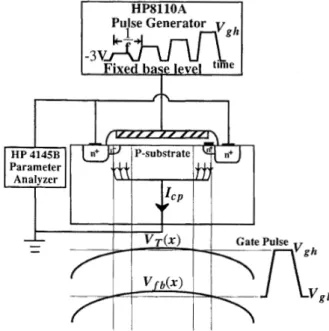
Fig. 1. Basic experimental set-up for charge pumping measurement.
aforementioned device degradation effect. In the past, most of the studies are concentrated on the individual study of Nit
characterization [2]-[4] and its correlation with the degra- dations [5] qualitatively. Only a few [6] are focused on the correlation between Nit, damaged region, Ldam and drain current degradation.
In this paper, we will develop a new characterization method to extract the spatial distribution of interface states using charge pumping measurement and the time-dependent power law relationship. Unlike other existing methods by adjusting the reversed drain bias V,,,, this method can directly profile the highly localized interface states as well as the effective time-dependent damaged length. For demonstration, this paper begins with the implementing details of this technique, along with some illustrative results. Next, this newly-developed method is applied to LDD n-MOSFET’s stressed at different biases so as to further investigate the device drain current degradation under long-term operating conditions.
11. DEVICE FABRICATION AND CHARGE-PUMPING MEASUREMENT
The LDD n-MOSFET’s used in this work were fabricated using a poly-Si gate twin-well CMOS process. The tested samples were 0.72-pm mask gate length (metallurgical junc- tion was 0.044-pm offset from gate edge), 20-pm channel width LDD transistors, 140-i% oxide thickness, and 0.15- pm conventional vapor-deposited sidewall oxide spacer. The channel was implanted with boron and followed by a diffu- sion process to adjust the channel to a surface concentration
N A = 1.5 x l O I 7 ~ m - ~ . After the conventional gate etching process, implantation with phosphorus dosage of 2 x 1013 cm-’ and energy 80 keV was performed in n- regions. Then, source and drain were arsenic-implanted with a junction depth of 0.22 pm. The required sourceldrain and channel
’ for 8 - 100 sec 200 sec 7 - 300sec 400 sec 1000 sec 2000 sec E! ‘2 I 3000sec 4 4000sec +3 ~ 5000sec 3 ~ 1OOOOse 12500 se 2 - 15000se h 4 6 - 500SeC 1 - v --3 2 - 1 0 1 2 3 4 5 Vgh (VI
Fig. 2. Measured Icp versus Vgh curves before and after various time stress The applied gate frequency 1s 1 MHz.
doping profiles for device simulations were generated using process simulator-SUPREM IV [7]. They were calibrated against SRP or SIMS data. In this work, we use PISCES IIB device simulator to simulate the majority-carrier distribution to define the effective channel length [8] that contributes to the measured charge-pumping currents.
The basic setup for charge pumping measurement is shown schematically in Fig. 1. We use a fixed base level CP mea- surement, i.e., the gate of an LDD n-MOS device under test is connected to a pulse generator (HP8110A), and the source/drain are grounded, while the substrate current is mea- sured. Note that the drain and source biases are held constant at zero to avoid the stress on devices during the measurement. A series of 1-MHz square pulse strings with rising/falling gradient of 25 n s N are used in our CP measurements. By fixing the base level
V,l
at - 3 V, we vary high level voltageV&
to measure CP currents for fresh and stressed LDD n- MOSFET’s. Fig. 2 shows the measured I,, versusV,,
curves with both source and drain grounded before and after various periods of channel-hot-carrier stress at VDS =7 V and VGS =6V for the tested sample. The dashed curve is the measured charge pumping current for a fresh device while the other solid curves are those for the device after different time stress. We can see that the CP currents rise abruptly when the applied high level gate voltages are larger than the local threshold voltage
VT(IC)
[4],
[9]-[ll], as shown in Fig. 1. With the increasing stress time, more interface states are generated and so are the CP currents. From this set of experimental data, we may further find a way to investigate the oxide damages associated with this hot-carrier-induced stress as described below.111. A NEW METHOD TO DETERMINE THE INTERFACE STATE AND THE DAMAGED REGION Although the charge pumping technique can be served as a good tool for characterizing the amount of interface states, it still has to be equipped with an appropriate method to enhance the characterizing capability. For this reason, here we will propose a new method to characterize the interface state distribution by combining the power-law model and the charge pumping measurement data. A general power-law formula for describing the time-dependent interface damages can be
900 IEEE TRANSACTIONS ON ELECTRON DEVICES, VOL. 43, NO 6, JUNE 1996 Stress @ VDs = I V, VGs = 6 V 0.9 - - - - - 7
I
+
0.8 0.7 0.6 X 0.5 0.4 0 3 10'Stress time (sec) Fig. 3.
damaged region along with the lateral surface electric field, is also shown.
Schematic diagram of the new characterization technique. The oxide Fig. 4.
law factor n is shown on the right.
Xcp.max versus stress time from Fig. 2. The time-dependent power
expressed as [ 121
In this equation, AIcp,max is the increase of the maximum CP current (i.e., a signal of the overall increase of the interface state density). q is the electron charge. A (A, and A h represent
the mean-free paths for electrons and holes, respectively,) is the mean-free path of the hot carrier.
E,
is the maximum lateral surface electric field.I D S
is the device drain current.W
is the gate width.C
is a proportional constant. The power-law factorn ( t )
indicates the power-law dependence on the stress timet ,
anddit
is a critical energy that a carrier must have in order to create interface traps. Let (bit,, and (bit.h be the criticalenergies for electrons and holes, respectively. Here, it should he noted that n has been modified to be a function of stress time (no longer assumed to be constant) and can be determined from experiment. Experimentally determined values for these parameters are = 3.7 eV and = 4.2 eV. Also, the values of the electron and hole mean-free paths are A, = 67
A
and Ah = 4 9 A [13], respectively.As described by Ancona et al. [14], in MOS devices with very thin gate oxides, the hot-carrier-induced interface state generation occurs in a relatively narrow zone (i.e., highly localized) and the peak is found to be well correlated with the location, where the lateral electric field reaches its maximum value. With this in mind and for simplicity, this highly localized interface trap ANi, (x) can be approximated by a rectangular distribution as shown in Fig. 3. Also, the approximate ANi, profile has the nonzero value
only in the effective damaged region. In the above equation,
f is the applied gate pulse frequency in CP measurement. The
effective time-dependent damaged length L d a m ( t ) is defined as the full width at half-maximum (FWHM) of the
AN,,
profile and can be regarded as an important index of the damage during hot-carrier stress. Here, it should he emphasized that our definition of Ldam(t) and the derivation of ANlt(Ic) are just based on the general feature of charge pumping method with an aim to reduce the repetitive CP measurements andcomplicated data manipulation as much as possible by making appropriate approximations.
Now, Ldarn(t) for (2) can be derived as follows. First, keeping the definition of FWHM in mind and referring again to the power-law expression, we get
Here, ANi, 1/2 is defined as one half of the maximum interface state generation AN;,
,
in tested device, and E1/2 is the lateral surface electric field at a location, where the induced amount of interface states is AN;t,1/2.Next, we can rearrange (3) to solve Eli2 which yields
=
(z
1+
qq&
q xql.
(4)The lateral surface electric field under the stress condition was simulated with a 2-D device simulator PISCES IIB [15]. To make sure that the simulation results are more convincing, the calibration procedure should be performed beforehand. Thus, the positions can be easily located from the simulated lateral surface electric field. As a consequence, the effective damaged length Ldam of the ANlt profile can be obtained by calculating the distance between the two E l l z locations as
illustrated in Fig. 3.
I v . RESULTS AND DISCUSSIONS
In Fig. 4, we show the increase (denoted by AIcp,max) of a sequence of the maxima in I,, (from Fig. 2) with stress time (in diamonds), which are plotted as a function of the stress time in log-log scale. They can be regarded as the changes of the induced interface states for the stressed and fresh devices. Initially, Alcp,max increases largely with the increasing stress time and then gradually saturates. According to the power-
law model, the power-law factor n ( t ) can he extracted from the slope of the log(Alcp,max) versus log(t) curve by (1) as shown also in Fig. 4 with solid circles. It can he seen that
n decreases largely with the increasing stress time, and then approaches to a saturated value, which is approximately 0.32 in this case. It has been reported that under the stress condition of the maximum substrate current bias (VGS E V&/2), the value of n is stress-bias dependent and is about 0.5, as in
LEE er al.: METHOD FOR CHARACTERIZING TIME-EVOLUTIONAL INTERFACE STATE 2.6 I
,
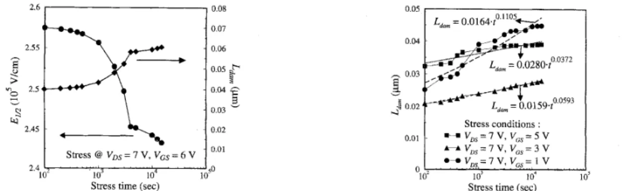
0.08 - 0.07 h v - 0.03 2.45 - - 0.01 Stress @ VDs = 7 V, VGs = 6 Vi 2 O
2.4 l? lo3 1 o4Stress time (sec)
0.07 2.5s i 0 . 0 6 w 2.5 0.04
-
f\
v V I'
2.45I
.
\
1
0.02 0.01 Stress @ VDs = 7 V, VGs = 6 V 2.4 l i lo3 1 o4Stress time (sec) Fig. 5 .
of FWHM.
E l / z and the effective damaged length Ldam versus time, in terms
2.2
I
2 8 Stress @ VD, = 7 V, VGS = 6 Vr, ] 2.4*
1.6 s 1.2 0.8 0.4 0, 3 v = O 0.1 0.2 0.3 0.4 0.5 0.6 0.7 0.8" Position (km) Fig. 6 .sponding lateral surface electric field distribution at the stress condition. Time evolution of lateral distributions of ANlt(z) and the corre-
[12]. However, when the device is stressed at other biases, n
is less than 0.5 as concluded in this work.
Before determining the effective damaged length Ldamr the corresponding lateral surface electric field distribution should be calculated first. Now, with this distribution being calculated by the 2-D device simulator, we can calculate Ellz (denoted in Fig. 3) straightforwardly from (4). The results are shown in Fig. 5. Values of EllZ decrease with the increasing stress time (i.e., with the decreasing power-law factor). Furthermore, with
E112 just obtained, we can find the two E112 positions from the simulated lateral surface electric field distribution. Thus, The effective damaged length Ldam of the AN,, profile with a full width at half-maximum (FWHM) can be obtained from the difference between the two E l l 2 locations. The results are again shown in Fig. 5.
Given
Alcp,max
andLdam,
the induced ANi, distribution can then be calculated from (2) as shown in Fig. 6. The simulated lateral surface electric field distribution Elat is also shown here. The insert shows the magnified box approximation with the magnitude ANi,, damaged region and damaged length Ldam near gate edge. From this figure, we can see that both the magnitude and damaged range ofANi,
increase with stress time while the damaged length tends to saturate gradually with stress time. It should be noted that if we keep the power- law factor n constant as one usually assumes, the effective damaged length is a constant at around 400A
in this case. This gives rise to a deviation of 2008,
by comparing with our calculations.Stress conditions :
10) 10'
Stress time (sec)
90 1
)i
Fig. 7. Time evolution of the damaged region length at various stress biases.
s = 7 v
."
0.68 0.7 0.72 0.74 0.76 Position (pm)
Fig. 8. Comparison of damaged regions for devices at different stress biases.
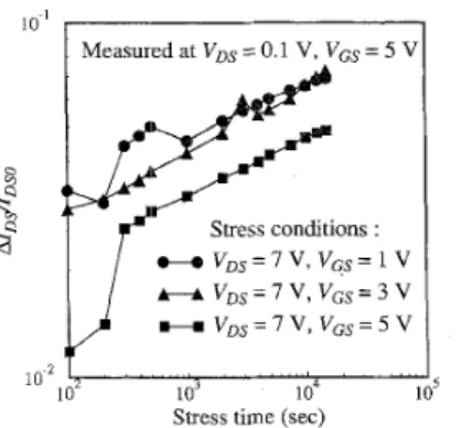
In order to further investigate the degradation in LDD n- MOSFET's, we also applied this method to tested devices under three different stress bias conditions (including VGS =
1, 3, 5 V, and VDS = 7 V). From Figs. 7 and 8, on one hand, we can see that the effective damaged length (most of which is located in the spacer region) is the shortest at
VDS
= 7 V and V i s = 3 V (or VGS E v&/2) among all the bias conditions, and initially Ldam at VDS = 7 V and VGS = 5 V is the largest. However, it turns out that Ldam at VDS = 7 V and VGS = 1 V is the largest in the long run. On the other hand, the smaller the gate voltage bias, the closer to drain side the damaged region. Although, at first the amount of interface states at VDs = 7 V andVGS
= 3 V is not the largest, due to the shortest Ldam it in turn leads to the rapid increase of interface states with stress time (shown in Figs. 9 and 10) and so enhances the degradation of drain current after a long time stress (shown in Fig. 11). In other words, for the devices stressed at the maximum substrate current (V& zV~s/2),
the oxide damage can be mainly attributed to interface trap generation through carriers [ 3 ] . For the comparison of growth rates in damagedlength and magnitude of interface trap, Fig. 12 shows the fitting parameters in Ldam and AN,, with a power form at different bias conditions. It reveals that with increasing stress time, the quantity
of
AN;,
at stress bias of VGS = 3V
is the largest finally. However, from the beginning of the stress (Fig. 9), the quantity of ANi, is not the largest. It means that in judging the current degradation in n-MOS devices, the criteria shouid consider both the combined effects of AN,,and oxide damaged region length Ldam. Based on the lateral surface electric field distributions and the time evolution of
902 IEEE TRANSACTIONS ON ELECTRON DEVICES, VOL. 43, NO. 6, JUNE 1996
Stress time (sec)
Fig. 9. Time evolution of ANit(2) at various stress biases.
.... 0.5 0.64 0.66 0.68 0.7 0.72 0.74 Position (Fm)
1
0.76 Fig. 10. and 15000 s.Lateral distributions of Al\*i,(z) at various stress biases for 100
power factors, it can be inferred that the effective damaged length in terms of FWHM will not necessarily increase with the increasing gate voltage bias.
To summarize, the advantages of the present method are listed below.
I ) In this experiment, we can easily obtain the lateral distribution of the induced
ANi,
along the channelmerely from one time-evolutional CP current Icp - Vgh, measured at 0-V drainkource bias. On one hand, because the drain and source are held constant at zero, this method can avoid changes of VT(Z) and V f i ( ~ ) during the inversion and accumulation half cycles. On the other hand, it requires no repetitive CP measurements, and hence avoids the likely imposition of re-stress on tested devices.
2) It can extract
AN;,
distribution directly from CP mea- surement without taking&,,
into account, even if it exists.3) It can even extract ANi, distribution outside of the contributed region that CP method can not detect. 4) This method can be generalized to calculate the lo-
cal ANit distribution along the whole channel region (including the source side).
v.
SUMMARY AND CONCLUSIONIn this work, a new method has been developed for char- acterizing the lateral distributions of interface states and the effective time-dependent damaged lengths. The correlation
Stress conditions :
w
f
Stress time (sec) Fig. 11.
stress biases for comparison.
Drain current degradations A I D s / I D s ~ versus time at various
0.12 I I 0.8 0.1 0.08
.
cl 0.02 n 0 1 2 3 4 5 6v,,
(VIFig. 12. Extracted parameters versus stress gate biases for Figs. 7 and 9. between the generated interface states with the stress time and the device drain current degradation can then be well described.
In this new method, by combining the power law as a function of stress time and the charge pumping measurement data, we can directly calculate the time-dependent effective damaged length and the spatial distribution of interface states with a rectangular approximation. To further investigate the device drain current degradation in terms of Ldam and
AN,,,
the damages of devices at different stress biases are analyzed in detail. It shows that for the devices stressed at the maximum substrate current (VGS M
VDs/2),
the effective damagedlength is the shortest. Moreover, device drain current degra- dation at this bias is the largest after
a
long period of stress since the generated interface state is most highly localized by comparing with the other stress biases.Owing to its simplicity, the developed method is expected to be useful for investigating the structure dependence of the hot carrier reliability in the drain engineering of submicron or deep-submicron VLSVULSI design. Moreover, this method can be used as a good and precise monitor of the hot carrier reliability in the state-of-the-art VLSIAJLSI device design.
REFERENCES
[ I ] K. R. Hofmann, C. Werner, W. Weber, and G. Dorda, “Hot-electron and hole-emission effects in short n-channel MOSFET’s,” IEEE Trans.
Electron Devices, vol. ED-32, p. 691, 1985.
[2] K. K. Ng and G. W. Taylor, “Effects of hot-carrier trapping in n- and p-channel MOSFET’s,” IEEE Trans. Electron Devices, vol. ED-30, p.
LEE et al.: METHOD FOR CHARACTERIZING TIME-EVOLUTIONAL 1NTERFACE STATE 903
[3] P. Heremans, R. Bellens, G. Groeseneken, and H. E. Maes, “Consis- tent model for the hot-carrier degradation in n-channel and p-channel MOSFET’s,” IEEE Trans. Electron Devices, vol. 35, p. 2194, 1988. [4] J. S . Brugler and P. G. A. Jespers, “Charge pumping in MOS devices,”
IEEE Trans. Electron Devices, vol. ED-16, p. 297, 1969.
[5] A. B. M. Elliot, “The use of charge pumping currents to measure surface state densities in MOS transistors,” Solid-State Electron., vol. 19, p.
241, 1976.
[ 6 ] K. T. San and T.-P. Ma, “Determination of trapped oxide charge in FLASH EPROM’s and MOSFET’s with thin oxides,” IEEE Electron Device Lett., vol. 13, p. 439, 1992.
[7] M. Law and R. W. Dutton, SUPREM IV, Stanford Univ., Stanford, CA,
1987.
[8] P. Heremans, J. Witters, G. Groeseneken, and H. E. Maes, “Analysis of the charge pumping technique and its application for the evaluation
of MOSFET degradation,” IEEE Trans. Electron Devices, vol. 36, p.
1318, 1989.
[9] M. Tsuchiaki, H. Hara, T. Morimoto, and H. Iwai, “A new charge pumping method for determining the spatial distribution of hot-carrier- induced fixed charge in p-MOSFET’s,” IEEE Trans. Electron Devices,
vol. 40, p. 1768, i993.
1101 G. Groeseneken, H. E. Maes, N. Bertran, and R. F. De Keersmaecker, “A .
-reliable approach to charge-pumping measurements in MOS transistors,”
IEEE Truns. Electron Devices, vol. ED-31, p. 42, 1984.
[ 111 W. Chen, A. Balasinski, and T.-P. Ma, “Lateral profiling of oxide charge and interface traps near MOSFET junctions,” IEEE Trans. Elecfron Devices, vol. 40, p. 187, 1993.
1121 C. Hu, S . C. Tam, F. C. Hsu, P. K. KO, T. Y. Chan, and K. W. Terrill, “Hot-electron-induced MOSFET degradation-Model, monitor, and improvement,” IEEE Trans. Electron Devices, vol. ED-32, p. 375,
1985.
[13] P. Heremans, G. van den Bosch, R. Bellens, G. Groeseneken, and H. E. Maes, “Temperature dependence of the channel hot-carrier degradation of n-channel MOSFET’s,” IEEE Trans. Electron Devices, vol. 37, p.
980, 1990.
1141 M. G. Ancona, N. S . Saks, and D. McCarthy, “Lateral distribution of hot-carrier-induced interface traps in MOSFET’ s,” IEEE Trans. Electron Devices, vol. 35, p. 2221, 1988.
1151 M. R. Pinto, C. S . Raffertv, H. R. Yeaper, and R. W. Dutton, “PISCES IIB-Poisson and continuity equation solver,” Standford Electronics Lab. Tech. Rep., Standford Univ., 1986.
Robert Giahn-Horng Lee wac born in Taipei, Tai-
wan, R . 0 C , in 1965 He received the B S degree in electrical engineering from National Cheng-Kung Univeryity, Taiwan, in 1987 and the M S degree in electronic engineering from National Chiao-Tung University, Hsinchu, Taiwan, in 1992. He is cur- rently working toward the Ph.D. degree at the Department of Electronic Engineering and Insti- tute of Electronics, National Chiao-Tung Univer- sity. His current research interests include CMOS VLSILJLSI technology, device design, device mod- eling and simulation, and hot carrier ctudy of miniaturized MOS devices.
Jiuun-Pey Wu was born in Taiwan, R O C , in
1971 He received the B S degree in electrical engineering from National Cheng-Kung University, Taiwan, in 1993 and the M S degree in electronic engineering from National Chiao-Tung University, Hsinchu, Taiwan, in 1995. His master thesis was on studying the gate-oxide dependence of the hot- carrier-induced degradation in submicron LDD n- MOS devices
Steve S. Chung (S’83-M’85-SM’95) received the B S degree from the National Cheng-Kung Univer- sity, Taiwan, in 1973, the M S c degree from the National Taiwan University, in 1975, and the Ph D degree from the University of Illinois at Urbana- Champaign, in 1985, all in electrical engineering
From 1976 to 1978, he worked for an electronic instrument company as Head of the R&D division and subsequently as Manager of the Engineering Division From 1978 to 1983, he was with the De- partment of Electronic Engmeeiing and Technology at the National Taiwan Institute of Technology (NTIT) as a Lecturer He was alqo in charge of an Instrument Calibration Center at NTIT From 1983 to
1985, he held a research aycistantship in the Solid State Electronics Laboratory and the Department of Electrical and Computer Engineering, University of Illinois In September 1985, he served at NTIT again as an Associate Professor in the Department of Electronic Engineering Since August 1987, he has been with the Department of Electronic Engineering and Institute of ElectronicT, National Chiao-Tung University, Hsinchu, Taiwan, and has been a Full Professor since the Fall of 1989 His current teaching and research interests are in the areas of solid-state device physics and VLSI technology, spice device modeling, numerical simulation and modehng of submicron and deep-submicron MOS devices, SO1 devices, nonvolatile memories and TFT’s, characterization and reliability study of VLSI devices and circuits, and computational algorithms for VLSI circuits. He has authored and co-authored more than 60 international journal and conference papery in the above area’,. Dr. Chung has served on various technical program committees of IEEE ASIC Conference ( U 3 ), International Electron Devices and Materials Sympo- sium (IEDMS, Taiwan), and HPC (High Performance Computing)-ASIA’95