This content has been downloaded from IOPscience. Please scroll down to see the full text.
Download details:
IP Address: 140.113.38.11
This content was downloaded on 25/12/2014 at 03:16
Please note that terms and conditions apply.
Gate-all-around floating-gate memory device with triangular poly-Si nanowire channels
View the table of contents for this issue, or go to the journal homepage for more 2014 Jpn. J. Appl. Phys. 53 04ED14
(http://iopscience.iop.org/1347-4065/53/4S/04ED14)
Gate-all-around
floating-gate memory device with triangular poly-Si nanowire channels
Jung-Ruey Tsai1*, Ko-Hui Lee2, Horng-Chih Lin2,3, and Tiao-Yuan Huang3
1Department of Photonics and Communication Engineering, Asia University, Taichung, Taiwan 413, R.O.C.
2Department of Electronics Engineering and Institute of Electronics, National Chiao Tung University, Hsinchu, Taiwan 300, R.O.C. 3National Nano Device Laboratories, Hsinchu, Taiwan 300, R.O.C.
E-mail: [email protected]
Received September 23, 2013; revised January 1, 2014; accepted January 28, 2014; published online March 24, 2014
A novel gate-all-around (GAA) poly-Sifloating-gate (FG) memory device with triangular nanowire (NW) channels was fabricated and characterized in this work. The enhanced electricfield around the corners of the NW channels boosts more electrons tunneling through the tunnel oxide layer during programming and erasing (P/E) processes, and thus the operation voltage markedly decreases. Furthermore, the nonlocalized trapping feature characteristic of the FG makes the injection of electrons easier during the programming operation, which was demonstrated by technology computer-aided design (TCAD) simulations. ©2014 The Japan Society of Applied Physics
1. Introduction
With the development of various portable electronic systems, the nonvolatile memory (NVM) has been utilized extensively for data storage because of its features of nonvolatility and low-power consumption. Among various NVM devices, the flash memory with the floating-gate (FG) structure is a mainstream product in the NVM market for decades.1–5)
However, the aggressive scaling trends in NVM devices push the conventional planar FG flash memory to face several severe challenges such as insufficient programming/ erasing efficiency, poor endurance, interference coupling between adjacent cells and power consumption. Hence, methods employing both poly-Si nanowire (NW) channel and three-dimensional gate-all-around (GAA) configurations to increase the programming and erasing (P/E) efficiencies are attractive owing to the enhancement of gate controllabil-ity over the channel and field strength near the channel surface.6–8) Nevertheless, P/E voltages are required to be
high (>17 V)3) to increase the surface electricalfield of the
channel and provide the channel electrons sufficient energy to overcome the barrier at the tunnel oxide/Si channel interface during the Fowler–Nordheim (FN) tunneling process. Since the electrical field in the corners of the NW channel is expected to be higher than those in the other regions of the NW channel, the sharper corner of the NW channel reasonably contributes to the higher surface electricalfield of the channel9)for lowering the operation voltage and meeting the need of lower power consumption. On the basis of the above motivations, we propose a scheme to fabricate a high-performance GAA FG poly-Si NW flash memory with triangular corners. The high P/E efficiency under low P/E voltages in the proposed memory device has been success-fully demonstrated in this work.
2. Experimental procedure
Figure 1 shows the schematic fabrication processes of the proposed FGflash memory device with a GAA poly-Si NW channel. An 80-nm-thick silicon nitride layer and a 150-nm-thick tetraethylorthosilicate (TEOS) oxide layer were depos-ited sequentially by low-pressure chemical vapor deposition (LPCVD) on thermally oxidized silicon substrates, as shown in Fig. 1(a). An undoped amorphous Si layer with a thickness of 100 nm was deposited by LPCVD and then subsequently annealed at 600 °C in N2 ambient for 24 h to transform the
poly-Si layer after lithographic patterning and dry etching processes of the top TEOS oxide layer, as illustrated in Figs. 1(b) and 1(c). Subsequently, the samples were im-planted with a high dose of 2© 1015cm¹2phosphorus ions at
25 keV. Note that low-energy ion implantation was carried out to obtain a high concentration of implanted dopants near the top surface of the poly-Si layer. After forming photoresist patterns on the poly-Si layer, the source/drain (S/D) regions were defined simultaneously with the NW channels abutting the sidewalls of the oxide layer during the reactive plasma etching process, as shown in Fig. 1(d). Note that the cross-sectional view of the resultant NW channel is triangular as obtained by sidewall spacer etching. The oxide and silicon nitride layers were selectively removed by wet etching to expose the NW channels following the S/D activation process, as shown in Fig. 1(e). Then, 11-nm-thick TEOS oxide, 25-nm-thick n+ poly-Si, 20-nm-thick TEOS oxide, and 150-nm-thick n+ poly-Si layers were sequentially deposited to form the tunnel oxide, FG, blocking oxide, and control gate (CG) regions, respectively, as shown in Fig. 1(f ). Finally, the control gate was defined and a standard metallization process completed the device fabrication. The schematic top-down and stereo views of the GAA NW FG memory structure are shown in Figs. 2(a) and 2(b), respectively. Figure 2(c) shows the scanning electron mi-croscopy (SEM) image of the top-down view of twin GAA NW devices. The channel length was estimated to be about
(a) (b) (c)
(d) (e) (f)
Fig. 1. (Color online) Schematic of fabrication processes of the GAA NW FG memory device.
Japanese Journal of Applied Physics 53, 04ED14 (2014) http://dx.doi.org/10.7567/JJAP.53.04ED14
REGULAR PAPER
400 nm, which is determined by the photomask utilized in the FG and SONOS devices. To benchmark the electrical performance of the proposed FG devices with 11-nm-thick tunneling oxide, 25-nm-thick poly-Si FG, and 20-nm-thick blocking oxide layers, GAA NW silicon–oxide–nitride– oxide–silicon (SONOS) memory devices with the same NW channels were fabricated simultaneously. The 3-nm-thick oxide, 7-nm-3-nm-thick silicon nitride, and 12-nm-3-nm-thick oxide layers were used as the tunneling oxide, trapping, and blocking oxide layers of the SONOS devices, respectively. 3. Results and discussion
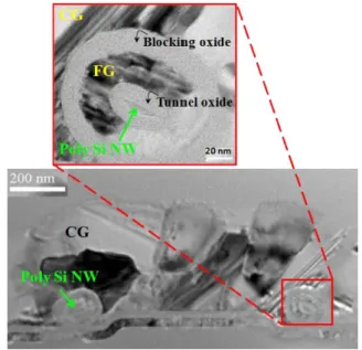
Figure 3 shows the cross-sectional transmission electron microscopy (TEM) images of the NW channels of the FG devices. The lengths of the three sides of a NW channel are
about 17, 17, and 30 nm, respectively (i.e., the total length of the triangular channel sides is approximately 64 nm). Figure 4(a) shows the experimental and simulated transfer characteristics of GAA NW flash memory devices with the FG and SONOS configurations. For simplicity, the threshold voltage (Vth) is defined as the gate voltage at a drain current
of 1© 10¹9A in these transfer curves measured at a drain voltage (Vd) of 0.1 V. Despite a large physical thickness of
about 55 nm for the gate dielectric in the FG device, a steep subthreshold swing (SS) of 112 mV/dec at Vd of 0.1 V, a
negligible DIBL, and a high Ion/Ioff current ratio of about
1© 108 at Vd of 1 V can be attributed to the GAA
con-figuration and thin NW channels. Similar electrical character-istics appeared in the transfer curve of the SONOS device measured at Vd of 0.1 V. According to the TEM image of
the triangular poly-Si NW channel, as shown in Fig. 3, the simulated device structures and electrical characteristics were obtained using a three-dimensional Sentaurus technology computer-aided design (TCAD) structure editor and a device simulator, respectively.10) The n-type doping concentration
in the channel was reasonably set to be 1© 1019cm¹2. The physical models used in the simulation include basic mobility models, such as doping dependence, normal/high electric field and velocity saturation, and tunneling/trap models. Regardless of the slopes of the transfer curves, the simulated threshold voltages well fit the experimental data of poly-Si NW devices with SONOS and FG structures by adjusting the negative fixed charge density of about 8 © 1012cm¹2at
the oxide/channel interface,11) as shown in Fig. 4(b). The
difference in slope between the transfer curves is mainly caused by the scattering of carriers due to the grain boundaries in the poly-Si NW channel.12)
Figure 5 depicts the P/E characteristics of GAA NW memory devices with FG and SONOS configurations under low programming and erasing operation voltages, ranging from 8 to 10 V and ¹6 to ¹8 V, respectively. The voltages applied in the terminals of the devices are listed in Table I. During the P/E operation, the operation voltage is applied to the CG of GAA NW devices while both the source and the
(a) (b) Source Drain NW L=0.4 µm (c)
Fig. 2. (Color online) (a) Top-down and (b) stereo views of the proposed GAA NW FG memory device. (c) SEM image of the top-down view of twin GAA NW devices.
Fig. 3. (Color online) Cross-sectional TEM pictures of triangular NW channel of a GAA NW FG memory device.
Jpn. J. Appl. Phys. 53, 04ED14 (2014) J.-R. Tsai et al.
drain are grounded. The starting threshold voltages before the programming and erasing operations are respectively 0.04 and 3.87 V for the SONOS device and 0.4 and 3.37 V for the FG device. Both the direct band-to-band (DT) and FN tunneling mechanisms were proposed to be responsible for the gate leakage. The DT tunneling of channel electrons usually occurs at a thin tunneling oxide layer (<2 nm), while the tunneling of electrons through a thick oxide layer is mainly caused by the FN tunneling mechanism.13) Addition-ally, for conventional FG devices, P/E operation voltages are set usually higher than 17 V to obtain a sufficient memory window evaluated using the shift in threshold voltage.3) As
compared with the SONOS device, the GAA NW FG device shows a greatly improved P/E efficiency. At a programming voltage of 10 V, the FG device achieves a shift in the threshold voltage of more than 2.5 V within 100 µs. Furthermore, as shown in Fig. 5(b), at an erasing voltage of¹8 V, the FG device shows an excellent erasing speed and also obtains a 2.5 V shift in threshold voltage within 100 µs. The fast and unsaturated Vth shift of the GAA NW FG
memory should be ascribed to the strong electricfield around the corners of the NW channels. The high P/E efficiencies under the low P/E voltages are realized in the GAA NW FG
memory but not in the GAA NW SONOS device. On the basis of the same NW channel configuration and similar transfer characteristics, as shown in Fig. 4, in the FG and SONOS devices, the gate-control channel abilities of both the FG and SONOS devices are similar in before programming. Hence, the difference in P/E efficiency between the FG and SONOS devices originates from the inherent characteristics of the charge storage materials, i.e., n+ poly-Si and silicon nitride.
Figure 6 illustrates the schematics of trapped electron profiles in the SONOS and FG devices, which were simulated at device programming times of 1© 10¹6 and 1© 10¹3s. The dielectric constants of the oxide and nitride layers are 3.9 and 7.5, respectively. The effective tunneling masses of electrons and holes in the nitride layer of the SONOS device are 0.36 and 0.38, respectively. Additionally, the trap concentration in the nitride layer is 4© 1019cm¹3 and
the capture cross section of an electron is set to be 5© 10¹16cm2.13,14)For the SONOS device, most of the electrons in the NW channel will tunnel into the nitride CT layer through the corners of the NW channel during device programming. Unlike the FG device, these tunneling elec-trons will be trapped locally in the nitride CT layer of the
10-6 10-5 10-4 10-3 0 1 2 3 4 5 Vg = 9 V Vg = 10 V Vth shift (V) Programming time (s)
Solid line : GAA NW FG device Dashed line : GAA NW SONOS device
(a) 10-6 10-5 10-4 10-3 -5 -4 -3 -2 -1 0 Vg = -7 V Vg = -8 V Vth shift (V) Erasing time (s)
Solid line : GAA NW FG device Dashed line : GAA NW SONOS device
(b)
Fig. 5. (Color online) Comparisons of (a) programming and (b) erasing characteristics of GAA FG and GAA SONOS memory devices with same NW channel dimensions.
Table I. Applied voltages in devices during P/E periods (in V). Gate voltage Drain voltage Source voltage
Program +9 or +10 0 0 Erase ¹7 or ¹8 0 0 10-14 10-12 10-10 10-8 10-6 10-4 -1 -0.5 0 0.5 1 1.5 2 2.5 GAA NW Flash L=0.4 mµ FG_Sim. Vd=0.1V SONOS_Sim. Vd=0.1V FG_Exp. Vd=0.1V FG_Exp. Vd=1V SONOS_Exp. Vd=0.1V
Drain Current (A)
Gate Voltage (V) (a) 0 5x10⁻⁵ 1x10⁻⁴ 1.5x10⁻⁴ 2x10⁻⁴ -1 -0.5 0 0.5 1 1.5 2 2.5 GAA NW Flash L=0.4 m FG_Sim. Vd=0.1V SONOS_Sim. Vd=0.1V FG_Exp. Vd=0.1V FG_Exp. Vd=1V SONOS_Exp. Vd=0.1V Drain Current 1/2 (A 1/2 ) Gate Voltage (V) (b) µ
Fig. 4. (Color online) Experimental and simulated transfer characteristics of the GAA NW FG and SONOS devices.
SONOS device near the corners of the NW channel owing to the fact that most of the trapping sites are discrete. The corresponding electric field distributions of poly-Si NW devices along the edge through the two sharp corners (along the XY direction, as shown in Fig. 6) of the NW channel in the SONOS and FG structures simulated at a programming voltage of +10 V with programming times of 1 © 10¹6and 1© 10¹3s are shown in Fig. 7. At the beginning of device programming, the maximum electric field was observed at the two sharp corners of NW channels near the tunneling oxide/NW interface in the NW devices. For the SONOS device, this maximum electric field decreases and the corresponding electricfield at the nitride CT/blocking oxide interface increases as the programming time increases to 1© 10¹3s. This clearly indicates that electrons have sufficient energies to surmount the barrier of the tunneling oxide layer and reach the nitride CT layer during device programming. After programming for 1© 10¹3s, the electric field at the tunneling oxide/NW interface is still higher than that at the nitride CT/blocking oxide interface, while the maximum electricfield of the NW FG device is observed at the blocking oxide/FG interface. As compared with the NW FG device, fewer tunneling electrons can be injected from the NW channel to the nitride CT layer owing to the low programming voltage and more localized trapping sites that exist in the nitride layer of the NW SONOS device.
The endurance and retention characteristics of GAA NW FG memories are shown in Figs. 8 and 9, respectively. In Fig. 8, the memory window closes after 1© 103 P/E cycles
since the strong electricfield around the sharp corners of the NW channel enhances the degradation of endurance perform-ance, which can be improved by optimizing the quality of the tunnel oxide layer.15) As compared with the measured
programming threshold voltage, the erasing threshold voltage increases obviously with the number of P/E cycles, resulting in the narrowing of the threshold voltage that may originate from the severe damage of the gate dielectric. The possible reason for this threshold voltage narrowing is the presence of electron traps in the tunneling oxide layer during the
programming state or hole traps in the tunneling oxide layer during the erasing state. Thus, it implies that the degradation of the gate dielectric tends to create hole traps in the tunneling oxide layer during P/E cycles.16) In Fig. 9, the
GAA NW FG device shows acceptable data retention performance owing to the sufficiently thick tunnel oxide layer and a 1.5 V memory window that remains after ten year extrapolation. Additionally, the much higher threshold voltage changes in the programming state than in the erasing NW SONOS CG 10-6 s Programming NW FG CG CG CG FG FG 10-6s Programming 10-3 s Programming 10-3s Programming X Y Y X X Y Y X
Fig. 6. (Color online) Schematic of trapped electron distributions in the GAA FG and SONOS devices simulated by Sentaurus TCAD simulator under the programming voltage of 10 V at programming times of 1© 10¹6 and 1© 10¹3s. 0 2x10⁶ 4x10⁶ 6x10⁶ 8x10⁶ 1x10⁷ 1.2x10⁷ 1.4x10⁷ 0.1 0.12 0.14 0.16 0.18 0.2 NW SONOS Electric Field (V/cm) X ( m)µ V g=10 V 1x10⁻⁶ s 1x10⁻³ s (a) O N O ON O
CG
CG
NW
0 2x10⁶ 4x10⁶ 6x10⁶ 8x10⁶ 1x10⁷ 1.2x10⁷ 1.4x10⁷ 0.08 0.12 0.16 0.2 0.24 NW FG Electric Field (V/cm) X ( m) V g=10 V 1x10⁻⁶ s 1x10⁻³ s (b) O O FG O FG OCG
CG
NW
µFig. 7. (Color online) Simulated electricfield distributions along the side edge through the two sharp corners of NW channel in the GAA FG and SONOS devices under the programming voltage of 10 V at programming times of 1© 10¹6and 1© 10¹3s. 100 101 102 103 104 0.0 0.5 1.0 1.5 2.0 2.5 3.0 Programming: Vg = 10 V, 0.2 msec Erasing: Vg = -8 V, 0.5 msec Vth (V) P/E Cycles
GAA NW FG
Fig. 8. (Color online) Endurance characteristics of a GAA NW FG memory device.
Jpn. J. Appl. Phys. 53, 04ED14 (2014) J.-R. Tsai et al.
state may due to more trapped electrons in the FG device when operated at the beginning of the programming state. 4. Conclusions
In this study, a simple method for the fabrication of a GAA poly-Si NW FG memory device with high P/E efficiency was successfully demonstrated. Owing to the stronger electric field around the channel corners and the nonlocalized trapping characteristics of the poly-Si FG, the GAA NW FG device shows superior P/E efficiency and memory window even under low operation voltages. This GAA NW FG device with triangular NW channels shows a high potential in future NORflash memory applications.
Acknowledgments
This work was sponsored in part by the National Science
Council, Taiwan (Nos. NSC-99-2221-E-009-167-MY3 and NSC-102-2221-E-468-028), the NCTU-UCB I-RiCE pro-gram (No. NSC-102-2911-I-009-301), and the Ministry of Education in Taiwan under the ATU Program, and the National Center, Taiwan, in supporting the high-performance computing for computer time and facilities.
1) S.-P. Sim, K. S. Kim, H. K. Lee, J. I. Han, W. H. Kwon, J. H. Han, B. Y. Lee, C. Jung, J. H. Park, D. J. Kim, D. H. Jang, W. H. Lee, C. Park, and K. Kim, Symp. VLSI Tech. Dig., 2006, p. 17.
2) S. S. Kim, W.-J. Cho, C.-G. Ahn, K. Im, J.-H. Yang, I.-B. Baek, S. Lee, and
K. S. Lim,Appl. Phys. Lett.88, 223502 (2006).
3) H.-T. Lue, P.-Y. Du, T.-H. Hsu, Y.-H. Hsiao, S.-C. Lai, S.-Y. Wang, S.-P. Hong, M.-T. Wu, F. H. Hsu, N. Z. Lien, C.-P. Lu, J.-Y. Hsieh, L.-W. Yang, T. Yang, K.-C. Chen, K.-Y. Hsieh, R. Liu, and C.-Y. Lu, IEDM Tech. Dig., 2009, p. 827.
4) M.-S. Seo and T. Endoh,Jpn. J. Appl. Phys.51, 02BD04 (2012).
5) C.-J. Su, T.-I. Tsai, H.-C. Lin, T.-Y. Huang, and T.-S. Chao,Nanoscale Res.
Lett.7, 339 (2012).
6) E.-K. Lai, H.-T. Lue, Y.-H. Hsiao, J.-Y. Hsieh, C.-P. Lu, S.-Y. Wang, L.-W. Yang, T. Yang, K.-C. Chen, J. Gong, K.-Y. Hsieh, R. Liu, and C.-Y. Lu,
IEDM Tech. Dig., 2006, p. 41.
7) W.-C. Chen, H.-C. Lin, Y.-C. Chang, and T.-Y. Huang,Appl. Phys. Lett.95,
133502 (2009).
8) S.-C. Chen, T.-C. Chang, P.-T. Liu, Y.-C. Wu, P.-H. Yeh, C.-F. Weng, S. M.
Sze, C.-Y. Chang, and C.-H. Lien,Appl. Phys. Lett.90, 122111 (2007).
9) S.-C. Chen, T.-C. Chang, P.-T. Liu, Y.-C. Wu, J.-Y. Chin, P.-H. Yeh, L.-W.
Feng, S. M. Sze, C.-Y. Chang, and C.-H. Lien,Appl. Phys. Lett.91, 193103
(2007).
10) Synopsis, Sentaurus Device H-2013.03 (March 2013).
11) H.-C. Lin, C.-I. Lin, Z.-M. Lin, B.-S. Shie, and T.-Y. Huang,IEEE Trans.
Electron Devices60, 1142 (2013).
12) P. M. Walker, S. Uno, and H. Mizuta,Jpn. J. Appl. Phys.44, 8322 (2005).
13) C.-H. Lee, S.-H. Hur, Y.-C. Shin, J.-H. Choi, D.-G. Park, and K. Kim,Appl.
Phys. Lett.86, 152908 (2005).
14) S.-D. Tzeng and S. Gwo,J. Appl. Phys.100, 023711 (2006).
15) U. Ganguly, T. Guarini, D. Wellekens, L. Date, Y. Cho, A. Rothschild, and
J. Swenberg,IEEE Electron Device Lett.31, 123 (2010).
16) T. Hayashi, Y. Kawazu, H. Fukuda, and T. Iwabuchi,Electron. Lett.29,
2178 (1993). 100 101 102 103 104 105 106 107 108 0 1 2 3 4 5 Programming: +10 V (5 ms) Erasing : -8 V (2 ms) Vth (V) Time (s)
GAA NW FG
initial 10 yearsFig. 9. (Color online) Retention characteristics of a GAA NW FG memory device.