國
立
交
通
大
學
電機學院 電子與光電學程
碩
士
論
文
擴散電阻的靜電放電特性分析與防護設計上的應用
ESD Characteristics of Diffusion Resistor and its Application in On-chip ESD
Protection
研 究 生:馮耀武
指導教授:柯明道 教授
擴散電阻的靜電放電特性分析與防護設計上的應用
ESD Characteristics of Diffusion Resistor and its Application in On-chip ESD
Protection
研 究 生:馮耀武 Student:Yao-Wu Feng
指導教授:柯明道 Advisor:Ming-Dou Ker
國 立 交 通 大 學
電機學院 電子與光電學程
碩 士 論 文
A ThesisSubmitted to Degree of Electrical and Computer Engineering National Chiao Tung University
in partial Fulfillment of the Requirements for the Degree of
Master of Science in
Electronics and Electro-Optical Engineering
January 2009
Hsinchu, Taiwan, Republic of China
擴散電阻的靜電放電特性分析與防護設計上的
應用
學生: 馮 耀 武
指導教授: 柯 明 道 教授
國立交通大學
電機學院 電子與光電學程碩士班
摘要
本論文是針對 silicided N+ 擴散電阻和 non-silicided N+ 擴散電阻在 100 奈 秒脈衝高電流加壓的條件下作出它的特性化和模型。經由實際量測,這兩種電阻 的阻值會隨著脈衝時間的方均根變化。在電阻上的電流會隨加壓時間增加而減 少、電阻上的電壓會隨加壓時間增加而增加。電阻在高電流下,造成非線性的電 壓-電流特性的原因可以用焦耳熱〈Joule-heating〉引起的電阻阻值改變來說明。 另外,本實驗所調查的這兩種電阻在高電流的條件下有不同的特性。因為這種不 同的特性,當這兩種電阻被應用在積體電路的靜電放電〈ESD〉防護上時,其所 實現的佈局設計要有所不同。ESD Characteristics of Diffusion Resistor and
its Application in On-chip ESD Protection
Design
Student: Yao-Wu Feng
Advisor: Prof. Ming-Dou Ker
Degree Program of Electrical and Computer Engineering
National Chiao-Tung University
ABSTRACT
The high current conduction in silicided N+ diffusion resistor and non-silicided N+ diffusion resistor under the 100nsec pulse condition had been characterized and modeled carefully in this work. We find the resistances of both types resistors change with the square root of the stress time. It induces the current decreasing and voltage increasing with the stress time. The root cause of the non-linear IV characteristics of the diffusion resistor under high current stress can be well explained by the Joule-heating induced the resistance change. In additional, we also find that these two diffusion resistors during high current stress will appear some different characteristics. Due to these different characteristics, the silicided device cannot use the same layout as the silicided blocking device on ESD protection design.
誌謝
首先我要感謝我的指導教授柯明道博士,在這六年半來所給予我的指導與鼓 勵。雖然在這段期間歷經工作上的壓力和家庭變故,使得在課業上斷斷續續。但 教授仍沒放棄指導,甚至經由教授的幫忙,讓我能夠兼顧工作與課業。教授要求 我追求研究的完整性與嚴謹性,使我體會到何謂研究。教授指導我做研究的方 向、方法、與態度,讓我對工作上的看法有了正面的改變。而這種改變也讓我在 工作上提升經驗值。教授的苦口婆心,到最後才真正的有所體悟,並且為此由衷 地感謝。 在這裡也要特別感謝台積電李建興經理。本篇論文是由李經理提供了 sample 讓我可以深入研究 diffusion resistor 的 ESD 特性及應用,也指導了我很多研究 diffusion resistor 相關的方向。另外,雖然跟他共事的時間只有短短的一年,但是 從他身上學到了很多東西;尤其半導體製程對 ESD 保護電路的影響,使我能將 所學與實務結合。李經理在 ESD 領域的豐富經驗,讓我縮短了對高壓製程 ESD 防護設計的學習曲線。不論在工作上或課業上,我從李經理身上獲益良多。 另外,我也要謝謝曾經在台積電的同事陳遂泓學長,楊道宏先生和 TRP 實 驗室的同仁吳偉豪、李仁豪、蔡柏豪。他們熱心教導我一些儀器的使用,使我能 在量測上順利取得實驗數據。並感謝吳國銘先生在製程上的協助。 感謝林昆賢博士對於高壓製程給予專業的解答,林群祐在論文撰寫格式上的 大力相助。另外也謝謝 307 研究室的所有同學和學長姐們。 我也感謝茂矽公司倪誠聰經理,也是他的鼓勵與支持才讓我有繼續進修的動 力。最後,我要感謝我的家人,尤其是我的太太李春櫻從未對我失去過信心。這 一直是我精神上最大的支柱。 還要感謝很多人,不可勝數,在此一併謝過,我會持續努力進步來達成大家 的期盼。 馮耀武 九十八年一月CONTENTS
ABSTRACT (CHINESE) ………...
i
ABSTRACT (ENGLISH) ……… ii
ACKNOWLEDGEMENT……… iii
CONTENTS……….. iv
TABLE CAPTIONS………. vi
FIGURE CAPTIONS………... vii
Chapter 1
Introduction………. 1
Chapter 2
Experiment………...………... 3
Chapter 3
Results And Discussions...………... 9
3.1 DCIVCHARACTERISTIC………..…... 9
3.2 HIGH CURRENT IVCHARACTERISTIC FOR RPON+DIFFUSION RESISTOR... 10
3.3 REAL-TIME IVCHARACTERISTIC FOR RPON+DIFFUSION RESISTOR…….. 11
3.3.1 Linear Region………... 11
3.3.2 Thermal Region……….………... 13
3.3.3 Saturation Region……….………... 15
3.3.4 Snapback Region……….. 16
3.4 HIGH CURRENT IV CHARACTERISTIC FOR SILICIDED N+ DIFFUSION RESISTOR……… 18 3.5 REAL-TIME IVCHARACTERISTIC FOR SILICIDED N+DIFFUSION RESISTOR. 19 3.5.1 Linear Region………... 20
3.5.2 Thermal Region……… 21
3.5.3 Saturation Region……… 22
3.6 ESDCOMPARISON FOR SILICIDED AND RPOGROUNDED-GATE NMOS….. 23
Chapter 4
Applications For On-chip ESD Protection Design….………….. 43
4.1 INPUT PIN ESDPROTECTION IMPROVEMENT…….……….. 43
4.2 OUTPUT PIN ESDPROTECTION IMPROVEMENT……...……… 44
Chapter 5
Conclusions……...….……….. 51
TABLE CAPTIONS
Table 3.1 Key layout parameter and ESD test result………. 26 Table 4.1 LVCESD structure splits ESD test result……….. 46 Table 4.2 LVCESD structure with chip splits ESD test result……….. 46
FIGURE CAPTIONS
Fig. 2.1 (a) Layout for RPO N+ diffusion resistor, (b) Cross-section for RPO N+ diffusion resistor………..…..….…………..………
5 Fig. 2.2 (a) Layout for Silicided N+ diffusion resistor, (b) Cross-section for
Silicided N+ diffusion resistor……….……….…... 6 Fig. 2.3 Apparatus for high current measurement……..………... 7 Fig. 2.4 Layout for (a) Silicided NMOS (W/L=720um/0.4um), (b) RPO
NMOS (W/L=300um/0.4um)………...……….... 8 Fig. 3.1 (a) DC IV Characteristics of a RPO N+ diffusion resistor vs.
temperature, (b) Resistance vs. temperature.………... 27 Fig. 3.2 (a) DC IV Characteristics of a Silicided N+ diffusion resistor vs.
temperature, (b) Resistance vs. temperature……… 28 Fig. 3.3 (a) Silicided N+ diffusion resistor has two conductor layers
(silicided film and N+ diffusion), (b) RPO N+ diffusion resistor only has one conductor layer (N+ diffusion).………... 29 Fig. 3.4 High current IV Characteristics of a RPO N+ diffusion resistor (a)
from linear region to snapback region, (b) from linear region to saturation region………... 30 Fig. 3.5 DC IV Characteristics of a RPO N+ diffusion resistor…….………... 31 Fig. 3.6 Linear region: (a) Voltage and Current waveforms, (b) Resistance
(V/I) and power (V×I) vs. time for a RPO N+ diffusion resistor under the 100nsec TLP pulse event………... 32 Fig. 3.7 Thermal region: (a) Voltage and Current waveforms, (b) Resistance
(V/I) and power (V×I) vs. time for a RPO N+ diffusion resistor under the 100nsec TLP pulse event…..……… 33 Fig. 3.8 Equivalent circuit of a RPO N+ diffusion resistor under the 100nsec
TLP pulse event………... 34 Fig. 3.9 Saturation region: (a) Voltage and Current waveforms, (b)
Resistance (V/I) and power (V×I) vs. time for a RPO N+ diffusion resistor under the 100nsec TLP pulse event……….…… 35 Fig. 3.10 Snapback region: (a) Voltage and Current waveforms, (b) Resistance
(V/I) and power (V×I) vs. time for a RPO N+ diffusion resistor under the 100nsec TLP pulse event……….. 36 Fig. 3.11 The current (a) before the snapback region, (b) at the snapback
region……… 37
Fig. 3.10………...……… 37 Fig. 3.13 (a) High current IV Characteristics of a Silicided N+ diffusion
resistor, (b) Zoom-In………...………. 38 Fig. 3.14 Linear region: (a) Voltage and Current waveforms, (b) Resistance
(V/I) and power (V×I) vs. time for a silicided N+ diffusion resistor under the 100ns pulse event………. 39 Fig. 3.15 Thermal region: (a) Voltage and Current waveforms, (b) Resistance
(V/I) and power (V×I) vs. time for a silicided N+ diffusion resistor under the 100nsec TLP pulse event…..……… 40 Fig. 3.16 Saturation region: (a) Voltage and Current waveforms, (b)
Resistance (V/I) and power (V×I) vs. time for a silicided N+ diffusion resistor under the 100nsec TLP pulse event………... 41 Fig. 3.17 High current IV characteristics of (a) silicided NMOS
(W/L=720um/0.4um), (b) RPO NMOS (W/L=300um/0.4um)…... 42 Fig. 4.1 Low trigger Voltage and low Capacitance ESD protection device
(LVCESD) (a) top view, (b) cross-section………... 47 Fig. 4.2 LVCESD splits (a) split structure, (b) TLP curve comparison………. 48 Fig. 4.3 LVCESD splits structure (a) LVCESD, (b) LVCESD with 10Ω N+
poly resistor, (c) LVCESD with 2nd ESD (Silicided NMOS W/L=20um/0.25um), (d) LVCESD with 2nd ESD (Silicided NMOS W/L=20um/0.25um) and 10Ω N+ poly resistor………...……… 49 Fig. 4.4 IV characteristics of a n+ diffusion resistor (W/L=5um/60um), (a)
Cathode and substrate(1) current vs. anode-to-cathode voltage, with the reverse-bias characteristics of the same well-substrate diode(2) added for reference, (b) The related static (Rs) and dynamic (Rd) resistance vs. anode-to-cathode voltage………... 49 Fig. 4.5 IV characteristics of a n-well diffusion resistor (W/L=70um/14um),
(a) Cathode and substrate current vs. anode-to-cathode voltage, (b) The related static (Rs) and dynamic (Rd) resistance vs. anode-to-cathode voltage………..…... 50 Fig. 4.6 Output buffer with a “decouple resistor”, (a) Main discharge through
a protection device N1, (b) Main discharge via the p-source to Vcc diode and the equivalent discharge path between the Vcc and Vss
Chapter 1
Introduction
The passive component (diffusion resistor) had been commonly used by the integrated circuit industry for a variety of applications. Most of these applications is related to low power operation, and as such, is not concerned the high current-level and the resulting effects. However, the diffusion resistor can be the component of the electrostatics discharge (ESD) protection circuit or is connected in series with output buffer to suppress the transition noise which are subjected to high current density level and the resulting effects.
The purpose of this work is to characterize and model the high current effects in the two common used diffusion resistors under a 100nsec transmission line pulse (TLP) condition and evaluate the electrical and thermal stability of the two diffusion resistors. Currently, there is limited information available on the high current and self-heating effects on these structures [1]-[2]. And, it can find an obvious error on the theoretical model for the diffusion resistor under the high current TLP stress event [2]. Although they had observed abnormal IV during the stress period, they still assume the stress current is a constant and does not vary with time during the stress period [2].
This paper will present a model based on Wunsch-Bell model [3] and identify important parameters related to the high current effects on the silicided diffusion resistor and silicided blocking (RPO) diffusion resistor. An understanding of these high current effects will enable the impact of technology scaling of silicided film to be
robust ESD protection device.
Chapter 2 describes two types of diffusion resistors’ structure and NMOS. Apparatus for high current measurement is also shown in this chapter. Chapter 3 shows the experimental results and discussion. There is a model built in this chapter. And make a comparison between silicided NMOS and non-silicided NMOS. Chapter 4 describes the resistor application on ESD protection. Chapter 5 is the conclusions of this thesis.
Chapter 2
Experiment
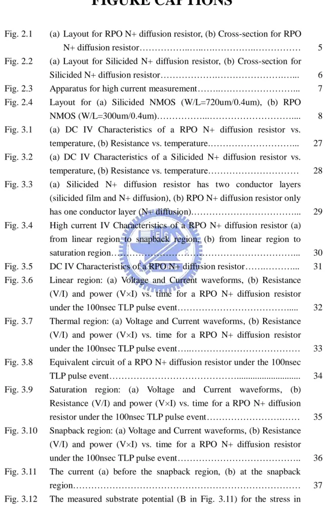
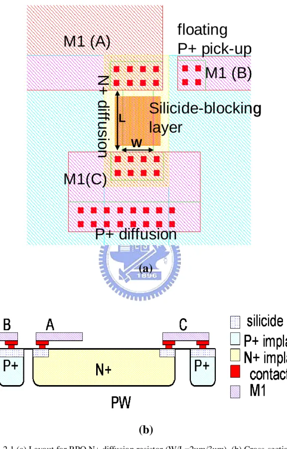
The technology used in this work is the 0.25-um CMOS silicided process. The silicided for this technology is Ti silicide (TiSi2). This technology also includes one silicided blocking (RPO) process to prevent the silicided film formation on the diffusion or poly if one wants to build the high resistance resistors in the chip for ESD purpose or circuit application. As a region is covered by the silicided blocking layer (RPO), this region will become a non-silicided region. The used resistors for this study are RPO N+ diffusion resistor (Fig. 2.1) and silicided N+ diffusion resistor (Fig. 2.2). The resistor has three terminals. The first terminal is used to apply the stress voltage (region A in Fig. 2.1 and Fig. 2.2). The second terminal is used to monitor the substrate potential of the diffusion resistor under the TLP stress event (region B in Fig. 2.1 and Fig. 2.2). The third terminal is the grounded terminal which includes a P+ diffusion and a N+ diffusion (region C in Fig. 2.1 and Fig. 2.2).
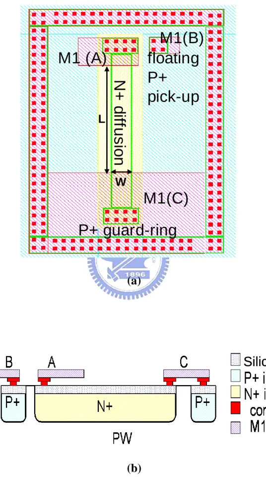
Fig. 2.3 shows the apparatus used for the high current IV characteristics measurement of the resistor under the TLP pulse. The TLP system is used for this measurement is the commercial Barth-TLP system. It can generate the 0.2nsec rising time and 100nsec pulse width single pulse and continuously increase the stress current up to 10A. The pulse is applied to one terminal of the resistor (region A) with respective to the grounded substrate and other terminal (region C). A 500MHz digital oscilloscope with 4G/sec sampling rate is used to capture the voltage, substrate potential, and current waveforms, simultaneously. The voltages are measured using
CT-1).
For silicided gate-ground NMOS and non-silicided (RPO) gate-ground NMOS, the layouts are shown in Fig. 2.4. The ESD performance comparison of these two devices is also presented in this report.
P+ diffusion
N
+
d
iff
us
io
n
Silicide-blocking
layer
M1(C)
M1 (A)
M1 (B)
floating
P+ pick-up
P+ diffusion
N
+
d
iff
us
io
n
Silicide-blocking
layer
M1(C)
M1 (A)
M1 (B)
floating
P+ pick-up
L
W
P+ diffusion
N
+
d
iff
us
io
n
Silicide-blocking
layer
M1(C)
M1 (A)
M1 (B)
floating
P+ pick-up
P+ diffusion
N
+
d
iff
us
io
n
Silicide-blocking
layer
M1(C)
M1 (A)
M1 (B)
floating
P+ pick-up
L
W
(a)
(b)
Fig. 2.1 (a) Layout for RPO N+ diffusion resistor (W/L=2um/3um), (b) Cross-section for RPO N+ diffusion resistor.
P+ guard-ring
N
+
d
if
fu
s
io
n
M1(C)
M1 (A)
M1(B)
floating
P+
pick-up
P+ guard-ring
N
+
d
if
fu
s
io
n
M1(C)
M1 (A)
M1(B)
floating
P+
pick-up
L
W
P+ guard-ring
N
+
d
if
fu
s
io
n
M1(C)
M1 (A)
M1(B)
floating
P+
pick-up
P+ guard-ring
N
+
d
if
fu
s
io
n
M1(C)
M1 (A)
M1(B)
floating
P+
pick-up
L
W
(a)
Silicide
Silicide
(b)
Fig. 2.2 (a) Layout for Silicided N+ diffusion resistor (W/L=2um/16.5um), (b) Cross-section for Silicided N+ diffusion resistor.
OD
Poly
RPO
Contact
OD
Poly
RPO
Contact
OD
Poly
RPO
Contact
(a)
(b)
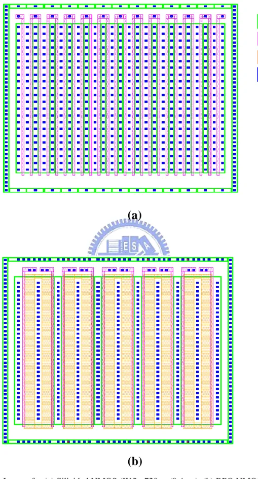
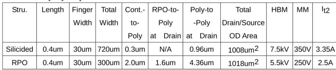
Fig. 2.4 Layout for (a) Silicided NMOS (W/L=720um/0.4um), (b) RPO NMOS (W/L=300um/0.4um).
Chapter 3
Results and Discussions
3.1 DC IV Characteristic
Fig. 3.1(a) and Fig. 3.2(a) show the DC IV characteristics of the RPO N+ diffusion resistor and silicided N+ diffusion resistor versus the temperature (25°C, 75°C and 125°C). The applied voltage is from 0V to 0.1V to make sure without Joule-heating generating during the measurement. So, the current can increase with the applied voltage linearly and decrease with the temperature. Fig. 3.1(b) and 3.2(b) show the resistances of the two kinds of the diffusion resistors versus the temperature based on above the measured results. The resistances for the two kinds of the diffusion resistors increase with the temperature linearly and follow the well known equation for the diffusion resistor.
R(T)=Ro(1+β T) (1) where R(T) is the dynamic resistance at temperature T(°C), β is the temperature coefficient of the diffusion resistor, Ro is the initial resistance at 0°C.
Based on this equation and the results in Fig. 3.1(b) and 3.2(b), the temperature coefficients are 0.00115/°C and 0.00360/°C for RPO N+ diffusion resistor and silicided N+ diffusion resistor, respectively. Although the sheet resistance of the RPO N+ diffusion resistor (115Ω/□) is much higher than that of the silicided N+ diffusion resistor (3.7Ω/□), the temperature coefficient of the RPO N+ diffusion resistor is smaller than that of the silicided N+ diffusion resistor. It is because that the silicided N+ diffusion resistor has two conduction layers (silicided film and N+ diffusion), but
in Fig. 3.3. And the more importance is that the silicided film is similar to a metal layer. So for silicided N+ diffusion resistor, most stress current will be confined in the small thickness silicided film, resulting in high current density. Compared with silicided N+ diffusion resistor, the current density of the RPO N+ diffusion resistor is smaller since the thickness of the N+ junction is thicker than that of the silicided film. Although the silicided N+ diffusion resistor has much higher current capability, ESD designer still uses the RPO N+ diffusion resistor to make the device ESD performance more robust.
3.2 High Current IV Characteristic For RPO N+ Diffusion Resistor
Fig. 3.4 shows the high current I-V characteristics of the RPO N+ diffusion resistor under the 100nsec TLP stress event. The set-up is shown in Fig. 2.3. A 100nsec current pulse is applied to one node of the RPO N+ diffusion resistor (A in Fig. 2.3) with respect to the grounded node of the RPO N+ diffusion resistor and P-substrate (C in Fig. 2.3). The stress current level is increased continuously until the RPO N+ diffusion resistor was damaged. The voltage and current waveforms of the RPO N+ diffusion resistor during the TLP stress period are measured simultaneously by the oscillator-scope during the TLP stress period. After each TLP stress, a DC meter is used to check the variation of the leakage current of the RPO N+ diffusion resistor for judging whether the RPO N+ diffusion resistor was damaged by the TLP stress or not. All measured data’s are transferred to a computer by an IEEE-488 cable. The computer records the data at 20nsec prior to the end of the TLP pulse and leakage current to the disk. Based on the recorded values at each stress level, the high current IV characteristics of the device are constructed as shown in Fig. 3.4.
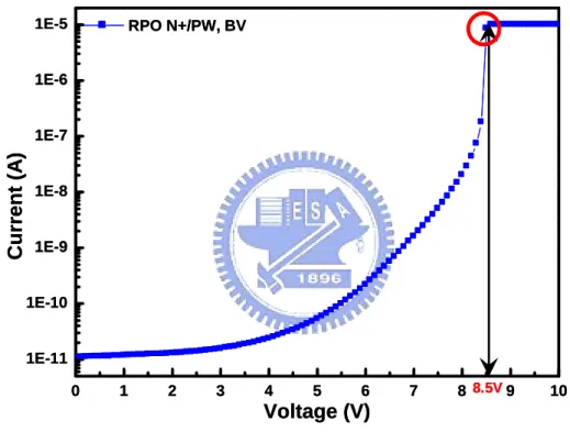
resistor can be divided by four regions (linear region, thermal region, saturation region and snapback region). For linear region, the current increases with the voltage linearly. Compared with linear region, the current in the thermal region only can slightly increase with the voltage. As it goes into the saturation region, the current cannot increase with the voltage any more. The current was clamped as a constant in this region until the applied voltage higher than the diffusion avalanche breakdown voltage. Fig. 3.5 shows the DC IV curve of the RPO N+ diffusion resistor. The current increases significantly if the applied voltage is higher than 8.5V. As the applied voltage is higher than the avalanche breakdown voltage, an apparent snapback phenomenon can be found in Fig. 3.4. The current at this region is higher than the saturation current. But, the voltage is smaller than the avalanche breakdown voltage.
3.3 Real-Time IV Characteristic For RPO N+ Diffusion Resistor
Because the high current IV curve only recodes a single point IV of the RPO N+ diffusion resistor under a 100nsec TLP stress event, it only can tell us that there are four different characteristics from low stress current to high stress current for the RPO N+ diffusion resistor but it cannot tell why it has the four different characteristics. In order to investigate the detail insight of a RPO N+ diffusion resistor under the TLP stress event, the voltage and current waveforms are used to analysis and see what is going on for a RPO N+ diffusion resistor under the TLP stress event.
3.3.1 Linear Region
Fig. 3.6(a) shows the current and voltage waveforms of the RPO N+ diffusion resistor in the linear region under a 100nsec TLP stress event. From 30nsec to 52nsec,
bounces back to the measured probes (Fig. 2.3). At this period, the voltage and current are the constants. Because of the difference in impedances between the cable and the test device, the pulse will be reflected based on the formula Γ=(ZL-ZO)/(ZL+ZO) [4] as the pulse reaches the device. The reflected wave will travel back to the TLP system [5]. As the reflected wave reaches the voltage probe and current probe, one may observe that voltage has increased sharply and current decreased sharply. This is because the pulse is a combination of a reflected wave and an incident wave. To do the TLP measurement, it needs the probe or wire as the inter-connector to connect the TLP system and the pad of the RPO N+ diffusion resistor. The probe or the wire acts as an inductor during the rising and falling stages of TLP stress pulse. This gives rise of the voltage (LdI/dt) and decreases the current when the pulse touches the RPO N+ diffusion resistor since the inductor current cannot be changed in an instant. After this transient (~52nsec), the pulse starts to stress the device. After 131nsec, there is no incident wave coming in from the TLP system and it has only a reflected wave traveling back from the device to the measurement probes as one may observe from the oscilloscope. One may observe that the current has decreased below 0A since by now only the reflected wave exists.
Based on the measured voltage and current in Fig. 3.6(a), the dynamic resistance (V(t)/I(t)) and the generated power (V(t)×I(t)) can be obtained as shown in Fig. 3.6(b). It can be found that the resistance and the generated power can keep as the constants at the TLP pulse stress period. Because this stress level only generates several milli-watt’s and the P-substrate can provide a good heating-sink source, the Joule-heating generated by the power can be transferred into the substrate completely and without leaving any Joule-heating in the RPO N+ diffusion resistor during the TLP pulse stress period. So, the temperature of the RPO N+ diffusion resistor can be
Based on eq. (1), the resistance will be a constant and the current can linearly increase with the voltage if the stress condition does not lead the RPO N+ diffusion resistor temperature increasing. This is why the current of the RPO N+ diffusion resistor can linearly increase with the voltage if it is biased at the linear region.
3.3.2 Thermal Region
Fig. 3.7(a) shows the thermal region current and voltage waveforms of the RPO N+ diffusion resistor under a 100nsec TLP stress event. It can be found that the current decreases and the voltage increases continuously during the TLP stress period. Based on the measured voltage and current in Fig. 3.7(a), the dynamic resistance (V(t)/I(t)) and the generated power (V(t)×I(t)) can be obtained as shown in Fig. 3.7(b). It can be found that the resistance increases and the generated power decreases with the TLP stress time. Because the generated power caused by this stress had reached several hundred milli-watt, the P-substrate cannot sink all Joule-heating generated from the power in an instant. As the RPO N+ diffusion resistor biased at the thermal region, part of the Joule-heating can be transferred into the P-substrate and part of the Joule-heating still left in the RPO N+ diffusion resistor to result in the increase in the temperature of the RPO N+ diffusion resistor. Fig. 3.8 shows the equivalent circuit of a RPO N+ diffusion resistor under the TLP stress event. The output resistance Rs of the TLP system is 50ohm. Unlike the resistance of the tested RPO N+ diffusion resistor varied with the TLP stress time, the TLP output resistance Rs does not vary with the stress current and can be treated as a constant resistance during the TLP stress period. And, the output voltage Vs of the TLP system during the TLP stress period can be treated as a constant voltage. Based on the equivalent circuit, the resistance change will cause the voltage and current varied with the TLP stress time.
)) ( /( ) ( ) (t VR t R R t V s s (3)
Based on Wunsch-Bell model [3], the increase in the temperature of a RPO N+ diffusion resistor under a square pulse is a function of the stress time and given by :
T(t)kP t (4) where generated power P can be approximated as a constant ( 0 0 2
2
)
/(R R
R
VS S )
during a square pulse.
Substituted eq.(4) into eq. (1), the dynamic resistance can be expressed as : R(t)R0(1a t) (5) where a=kβ P.
So, the current varied with the stress time can be expressed as :
I(t)Vs/(Rs R0(1a t)) (6) And, the voltage varied with the stress time can be expressed as :
V(t)VsR0(1a t)/(RSR0(1a t)) (7) From eq. (4), we know that the Joule-heating caused by the generated power (P) will induce the temperature of the RPO N+ diffusion resistor increasing. And, the increase in the RPO N+ diffusion resistor temperature will cause the resistance increasing based on eq. (1). From eq. (5), the resistance of a RPO N+ diffusion resistor under a TLP stress increases with the square root of the stress time. Fig. 3.7 shows that the calculated resistance based on eq. (5) can fit the measured resistance. Based on eq. (6) and eq. (7), the increase in the resistance will induce the voltage increasing and current decreasing as the observed result in Fig. 3.7(a). All the calculated values based on eq. (6) and eq. (7) can fit the measured curves very well. Based on eq. (1) and the result in Fig. 3.7(b), this stress will lead in the temperature of the RPO N+ diffusion resistor increasing about 470°C at the end of the pulse.
3.3.3 Saturation Region
Fig. 3.9(a) shows the current and voltage waveforms of the RPO N+ diffusion in the saturation region resistor under a 100nsec TLP stress event. Compared with the thermal region current (45mA to 30mA), the decrease in the magnitude of the current (50mA to 30mA) is more sharply. It can be found that the generated power (0.35W) for the thermal region is higher than that (0.27W) of the thermal region (Fig. 3.9(b)). The higher the power is, the higher the Joule-heating leaves in the RPO N+ diffusion resistor to cause the higher increase in the temperature of the RPO N+ diffusion resistor. Based on eq. (1) and the result in Fig. 3.9(b), this stress will lead in the temperature of the RPO N+ diffusion resistor increasing about 690°C at the end of the pulse.
Same behavior as the RPO N+ diffusion resistor in the thermal region, the resistance increases with the square root of the TLP stress time followed the eq. (5) as shown in Fig. 3.9(b). As the resistance increases with the square root of the TLP stress time, it will induce the stress current decreasing and voltage increasing continuously with the TLP stress time (Fig. 3.9(a)) which follows the eq. (6) and (7).
By comparing the Fig. 3.7(a) and Fig. 3.9(a), it can be found that the initial current and voltage (~52nsec in Fig. 3.7(a) and 3.9(a)) can increase with the applied voltage Vs. Subsequently, the current decreases and voltage increases with the TLP stress time continuously following the above equations. Because the resistance increase follows the square root term of the TLP stress time, the resistance curve will show a sharp rising slop at the beginning of the pulse (52nsec~80nsec) and become flat at the end of the pulse (100nsec~132nsec). It is worth noting that the high current IV (Fig. 3.4(a)) only records the measured point prior to the end of the pulse 20nsec. From eq. (6), the current is a function of the applied voltage Vs divided by the
resistance is a function of the applied voltage based on eqs. (1) and (4) and can be expressed as : ) ) /( 1 ( ) (t R0 kV2R0 t R R0 2 R S S (8) At the beginning of the stress pulse, the second term is small and can be neglected. So, the stress current still increases with the applied voltage. As the stress time is long enough, the second term of eq. (8) becomes important. It can compensate the increase in the current caused by the applied voltage, resulting in the current independent of the applied voltage. So, the stress voltage still can increase with stress voltage, but the stress current will be clamped to a constant for the longer time stress. This is why the high current IV (Fig. 3.4) shows that the current cannot be increased at the saturation region. If the recording data point is at other region, the high current IV curve of the RPO N+ diffusion resistor will not appear the saturation characteristic.
3.3.4 Snapback Region
Fig. 3.10(a) shows the current and voltage waveforms of the RPO N+ diffusion resistor in the snapback region under a 100nsec TLP stress event. For this stress, the applied voltage (~9V) in the initial transient (50nsec~95nsec) is apparently higher than the breakdown voltage of the N+ diffusion 8.5V based on the DC IV measured result in Fig. 3.5. Unlike the stress currents of the linear region, thermal region and saturation region, the current of the snapback region cannot be confined in the RPO N+ diffusion resistor any more. Most of the current still flows through the RPO N+ diffusion resistor, but part of the current flows into the P-substrate and through the P-Well resistor (R-sub) to Vss (Fig. 3.11(a)). This gives rise of the substrate potential as shown in Fig. 3.12. In this test structure, a floating P+ pick-up (Fig. 2.2) is designed to monitor the P-substrate potential variation of the RPO N+ diffusion
resistor during the TLP stress period. The set-up for substrate potential is shown in Fig. 2.3.
Like the behavior of the thermal region and saturation region, the RPO N+ diffusion resistor resistance increases with the stress time caused by the RPO N+ diffusion resistor temperature increasing due to power induced the Joule-heating generation (Fig. 3.12). The increase in the RPO N+ diffusion resistor resistance will decrease the current flowing through the RPO N+ diffusion resistor to push more current flowing into the P-substrate, resulting in the substrate potential increasing gradually as shown in Fig. 3.12 (50nsec~95nsec). As the substrate potential reaches the critical point (0.7V at the stress time 95nsec in Fig. 3.12), the junction between the P-substrate and the cathode of the RPO N+ diffusion resistor will be forwarded, resulting in the cathode of the RPO N+ diffusion resistor injecting the electrons. These injected electrons will be collected by the anode of the RPO N+ diffusion resistor. This action can be treated as the npn bipolar turned on (Fig. 3.11(b)). As the npn bipolar turned on, it can provide a very low impedance conduction path to sink much more than the current that the RPO N+ diffusion resistor can sink. The resistor during the snapback region can be treated as a RPO N+ diffusion resistor and on resistor of an npn bipolar in parallel. But, the on resistor resistance of an npn bipolar is much smaller than the RPO N+ diffusion resistor resistance. We can find the resistance during the snapback region is apparently is much smaller than that of the region before occurred the snapback. This induces the current increasing and voltage decreasing drastically. So, an apparent snapback phenomenon can be found after the transient 95nsec in Fig. 3.11(a). Then, a lot of current will flow though the P-substrate to result in the substrate potential at region B in Fig. 3.11 increases sharply.
3.4 High Current IV Characteristic For Silicided N+ Diffusion
Resistor
Fig. 3.13 shows the high current I-V characteristics of a silicided N+ diffusion resistor under the 100nsec TLP stress event. The set-up is shown in Fig. 2.3. A 100nsec current pulse is applied to one node of the silicided N+ diffusion resistor (A in Fig. 2.3) with respective to the grounded node of the silicided N+ diffusion resistor and P-substrate (C in Fig. 2.3). The stress current level is increased continuously until the silicided N+ diffusion resistor was damaged. The voltage and current waveforms of the silicided N+ diffusion resistor during the TLP stress period are measured simultaneously by the oscillator-scope. After each TLP stress, a DC meter is used to check the variation of the leakage current of the silicided N+ diffusion resistor for judging whether the silicided N+ diffusion resistor was damaged by the TLP stress or not. All measured data’s are transferred to a computer by an IEEE-488 cable. The computer records the data at 20nsec prior to the end of the TLP pulse and leakage current to the disk. Based on the recorded values at each stress level, the high current IV characteristics of the device are constructed as shown in Fig. 3.13.
Although the high current IV characteristics of the silicided N+ diffusion resistor also can be divided by four regions, it does not be found the snapback phenomenon even at high current stress level. The four regions for silicided N+ diffusion resistor are linear region, thermal region, saturation region and breakdown region. For linear region, the current increases with the voltage linearly. Compared with the linear region, the rising slop of the current at the thermal region is more gradient. As it goes into the saturation region, the current cannot increase with the voltage any more. It is worth noting that the saturation current for silicided N+ diffusion resistor (135mA) is larger than that of the RPO N+ diffusion resistor (33mA) since the silicided N+
the current conduction capability of silicided film is higher than that of RPO N+ diffusion.
Unlike the RPO N+ diffusion resistor that can be driven into the snapback when the applied voltage higher than the junction avalanche breakdown voltage, the current for the silicided N+ diffusion resistor still can be kept as a constant even the applied voltage higher than the junction avalanche breakdown voltage (8.5V as shown in Fig. 3.5). This difference is caused by that the two test structures have different P+ diffusion layouts. For RPO N+ diffusion resistor, the P+ diffusion used as the ground is below the cathode of the RPO N+ diffusion resistor (Fig. 2.2). For silicided N+ diffusion resistor, the P+ diffusion used as the ground is a guard-ring which surrounds the silicided N+ diffusion resistor completely. This kind layout will decrease the resistance of the substrate resistor (Rsub in Fig. 3.11(a)) significantly to result in the turn-on condition for a bipolar (Isub× Rsub) hard to achieve. So, the snapback phenomenon cannot be found and the silicided N+ diffusion resistor only can be biased at avalanche region if the applied voltage is higher than the junction breakdown voltage.
3.5 Real-Time IV Characteristic For Silicided N+ Diffusion Resistor
Same reason as we talked in the RPO N+ diffusion resistor, a single recoding point IV can not tell us what’s going on of the silicided N+ diffusion resistor during the TLP stress event. So, the whole voltage and current waveform are used to investigate the detail insight of a silicided N+ diffusion resistor under the TLP stress event.
3.5.1 Linear Region
Fig. 3.14(a) shows the current and voltage waveforms of the silicided N+ diffusion resistor in the linear region under a 100nsec TLP stress event. From 25nsec to 52nsec, the pulse travels through the measured probes to the silicided N+ diffusion resistor and bounces back to the measured probes (Fig. 2.3). At this period, the voltage and current are the constants. Compared the Fig. 3.6(a) and Fig. 3.14(a), the voltage waveform of the silicided N+ diffusion resistor during the TLP stress period is apparently different from that of the RPO N+ diffusion resistor during the TLP stress period. It is because of that the resistance of the silicided N+ diffusion resistor (~30Ω) is smaller than the TLP output resistance (50Ω), but the resistance of the RPO N+ diffusion resistor (~170Ω) is much larger than the TLP output resistance (50Ω). Except the resistor resistance, the inductance caused by the bonding wire or probe is needed to count into the impedance for the loading (ZL). But, it is well known that the impedance caused by the inductance is arisen from LdI/dt. So, it only can affect the voltage waveform at the beginning of the TLP stress due to large dI/dt (B in Fig. 3.14(a)), but can be neglected after this transient due to nearly zero dI/dt.
Adding the inductance will cause the loading impedance ZL larger than the TLP output resistance to generate a positive reflected wave based on the formula Γ=(ZL-Z0)/(ZL+Z0), resulting in the voltage higher than the initial voltage (Vi in Fig. 3.14(a)). Without the inductance, the impedance of the silicided N+ diffusion resistor becomes smaller than the TLP output resistance to induce a negative reflected waveform, resulting in the voltage smaller than the initial voltage (Vi in Fig. 3.14(a)). Based on the measured voltage and current in Fig. 3.14(a), the dynamic resistance (V(t)/I(t)) and the generated power (V(t)×I(t)) can be obtained as shown in Fig. 3.14(b). It can be found that the resistance and the generated power all can keep
power is still quite low and all can be transferred into the substrate completely. Without the additional heat, the silicided N+ diffusion resistor temperature does not vary with the TLP stress time and the resistance can keep as the constant based on eq. (1). So, the current of the silicided N+ diffusion resistor can linearly increase with the voltage as it is biased at the linear region.
3.5.2 Thermal Region
Fig. 3.15(a) shows the current and voltage waveforms of the silicided N+ diffusion resistor in the thermal region under a 100nsec TLP stress event. It can be found that the current decreases and the voltage increases continuously during the TLP stress period. Based on the measured voltage and current in Fig. 3.15(a), the dynamic resistance (V(t)/I(t)) and the generated power (V(t)×I(t)) can be obtained as shown in Fig. 3.15(b). It can be found that the resistance increases with the TLP stress time and the generated power is nearly a constant during the TLP stress period. Same mechanism as the discussion in the thermal region for RPO N+ diffusion resistor, the P-substrate can not sink all Joule-heating generated from the power in an instant to leave part of Joule-heating in the silicided N+ diffusion resistor, resulting in the increase in the temperature of the silicided N+ diffusion resistor. The detail mechanism that the current and voltage varied with the TLP stress time had been discussion in the section of the thermal region for RPO N+ diffusion resistor. Based on eq.(1) and the result in Fig. 3.15(b), this stress will lead in the temperature of the silicided N+ diffusion resistor increasing about 139°C. Compared with the RPO N+ diffusion resistor, the temperature increase at the thermal region for the silicided N+ diffusion resistor is nearly 1/3 of the temperature increase for the RPO N+ diffusion resistor since the temperature coefficient of the silicided N+ diffusion resistor is
3.5.3 Saturation Region
Fig. 3.16(a) shows the saturation region current and voltage waveforms of the silicided N+ diffusion resistor under a 100nsec TLP stress event. Compared with the current in the thermal region (108mA to 99mA), the saturation current decreases more sharply (148mA to 113mA). The generated power (~1W) during the saturation region (Fig. 3.16(b)) is nearly twice of the generated power (0.5W) during the thermal region (Fig. 3.15(b)). The more power is generated, the more Joule-heating leaves in the silicided N+ diffusion resistor to induce in the higher temperature for the silicided N+ diffusion resistor. Based on eq. (1) and the result in Fig. 3.16(b), this stress will lead the temperature of the silicided N+ diffusion resistor increasing about 224°C at the end of the pulse which is much higher than the increase in the temperature of the silicided N+ diffusion resistor during the thermal region (139°C), but much smaller than the increase in the temperature of the RPO N+ diffusion resistor during the saturation region (690°C). Fig. 3.16(b) shows that the silicided N+ diffusion resistor also can follow eq. (6) which resistance increases with the square root of the stress time. Thus, the current and voltage also can follow the eqs. (7) and (8) to increase and decrease with the stress time, respectively. By comparing Figs. 3.7(b) and 15(b) or Figs. 3.9(b) and 16(b), it can be found that the generated power for silicided N+ diffusion resistor during the TLP stress period is nearly a constant that does not vary with the stress time, while the generated power for the RPO N+ diffusion resistor during the TLP stress period decreases with the stress time. It implies that the thermal conduction for RPO N+ diffusion resistor is better than the silicided N+ diffusion resistor. The more heat transferred into the P-substrate, the less power left in the RPO N+ diffusion resistor. So, the generated power will decrease with the stress time. The less heat transferred into the P-substrate, the more power left in the silicided N+
difference might be caused by that the current of the silicided N+ diffusion resistor is confined in the thin silicided film to induce the local heating, but the current of RPO N+ diffusion resistor can flow whole junction and the junction is just above the large heat-sink P-substrate. Because the Joule-heating induced the device temperature increasing higher than the silicon melting point is the main cause of the ESD failure, the device will have poor ESD performance if it has the bad thermal conductivity. This is why we often think that the silicided process will degrade the device ESD performance.
3.6 ESD Comparison For Silicided And RPO Grounded-Gate NMOS
The self-protection scheme, which N/PMOS drivers are the ESD protection devices, is commonly used for digital I/O ESD protection. Using this scheme, the NMOS will dominate the ESD event. So, NMOS is much more important than the PMOS for I/O ESD protection in CMOS technology. Up to now, ESD designers often have the concept that the silicided process will degrade the device ESD performance. So, various schemes from process (silicided block (RPO) [6]) and circuits (gate coupling [7] and substrate trigger [8]) are proposed to improve the NMOS ESD performance. But, the RPO scheme seems more popular than other schemes since most foundries provide the RPO design rules for customers as the reference. And, most ESD designers accept the concept that RPO can build a ballast resistor [9] for NMOS. But, most people do not know why NMOS needs a ballast resistor drain. In fact, the ESD event can be treated as a constant current stress event. Whether the device has a ballast resistor cannot change the ESD stress current level [10] and the current capability of the silicided N+ diffusion resistor is apparently much higher than
N+ diffusion resistor can sustain more current than the RPO N+ diffusion resistor, it does not have the reason that the silicided device is more vulnerable to ESD stress than the RPO device. So, the ballast resistor concept cannot explain why using RPO to forbid the silicided formation on the drain can improve the device ESD performance. In fact, we find the silicided device can be designed as robust as or even better than the RPO device.
As we discussed in the above sections, we can conclude some different characteristics for RPO N+ diffusion resistor and silicided N+ diffusion resistor : 1. the thermal conductivity of the RPO N+ diffusion resistor is better than the silicided N+ diffusion resistor, 2. the saturation current of the silicided N+ diffusion resistor is higher than that of RPO N+ diffusion resistor, 3. for silicided N+ diffusion resistor, most current will be confined in the silicided film, 4. for RPO N+ diffusion resistor, the current can distribute whole junction. Because of these different behaviors, the silicided grounded-gate NMOS (GGNMOS) and RPO GGNMOS cannot use same kind layout if one wants to get good ESD performance for these two devices.
Fig. 2.4 shows the layouts of these two devices. Table 3.1 lists the key parameters and ESD test results for these two devices. The dimensions for these two devices are almost the same (silicided GGNMOS 30×33.6=1008um2, RPO GGNMOS 30×33.95=1018.5um2). Based on characteristic 4, the current of the RPO N+ diffusion resistor can distribute whole junction, we use long contact to poly space on the drain (RPO=1.6um) to get larger drain junction (4.36×30×5=654um2), compare with the silicided device (0.96×30×12=345.6um2). Based on characteristic 3, most current of the silicided N+ diffusion resistor will be confined in the silicided film, the junction is useless for the silicided device ESD protection. So, we need to increase total drain junction perimeter of the silicided device instead of using larger device drain junction
to P-substrate. The total perimeter of the drain junction for the silicided GGNMOS (30×12×2=720um) is nearly two and a half of the RPO GGNMOS (30×5×2=300um).
Based on above design concept, both devices all can get better ESD performances that can pass HBM 2KV and MM 200V industry specification (Table 3.1). And, it is worth noting that ESD performance of the silicided GGNMOS is more robust than the RPO GGNMOS. For the silicided GGNMOS, it can pass HBM 7.5KV, MM 350V and It2 3.35A. For the RPO GGNMOS, it can pass HBM 5.5KV, MM 250V and It2 2.5A. Fig. 3.17 shows the high current IV characteristics of the silicided GGNMOS and RPO GGNMOS. It can be found that the silicided GGNMOS has smaller Ron and higher It2, compared with the RPO GGNMOS. For same dimension, the ESD performance for the silicided GGNMOS can be designed higher than 30% of the RPO GGNMOS in 0.25um CMOS process. The comparison of silicided and non-silicided GGNMOS in series with a resistor between gate and ground is the future work in other process.
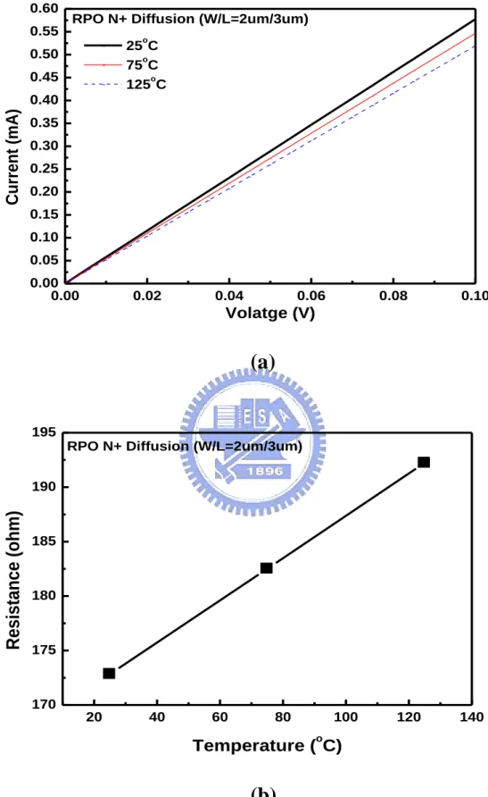
Table 3.1 Key layout parameter and ESD test result.
Stru. Length Finger Width Total Width Cont.- to- Poly RPO-to- Poly at Drain Poly-to -Poly at Drain Total Drain/Source OD Area HBM MM It2
Silicided 0.4um 30um 720um 0.3um N/A 0.96um 1008um2 7.5kV 350V 3.35A RPO 0.4um 30um 300um 2.0um 1.6um 4.36um 1018um2 5.5kV 250V 2.5A
0.00 0.02 0.04 0.06 0.08 0.10 0.00 0.05 0.10 0.15 0.20 0.25 0.30 0.35 0.40 0.45 0.50 0.55 0.60
RPO N+ Diffusion (W/L=2um/3um)
Cur rent (mA ) Volatge (V) 25oC 75oC 125oC
(a)
20 40 60 80 100 120 140 170 175 180 185 190 195RPO N+ Diffusion (W/L=2um/3um)
Res
istance (ohm
)
Temperature (oC)
(b)
Fig. 3.1 (a) DC IV Characteristics of a RPO N+ diffusion resistor vs. temperature, (b) Resistance vs. temperature.
0.00 0.02 0.04 0.06 0.08 0.10 0.0 0.5 1.0 1.5 2.0 2.5 3.0 C ur ren t ( mA ) Volatge (V)
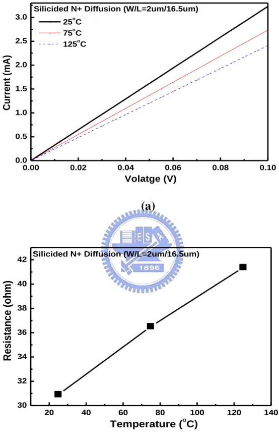
Silicided N+ Diffusion (W/L=2um/16.5um)
25oC 75oC 125oC
(a)
20 40 60 80 100 120 140 30 32 34 36 38 40 42Resi
stan
ce
(oh
m)
Temperature (oC)Silicided N+ Diffusion (W/L=2um/16.5um)
(b)
Fig. 3.2 (a) DC IV Characteristics of a Silicided N+ diffusion resistor vs. temperature, (b) Resistance vs. temperature.
(a)
(b)
Fig. 3.3 (a) Silicided N+ diffusion resistor has two conductor layers (silicided film and N+ diffusion), (b) RPO N+ diffusion resistor only has one conductor layer (N+ diffusion).
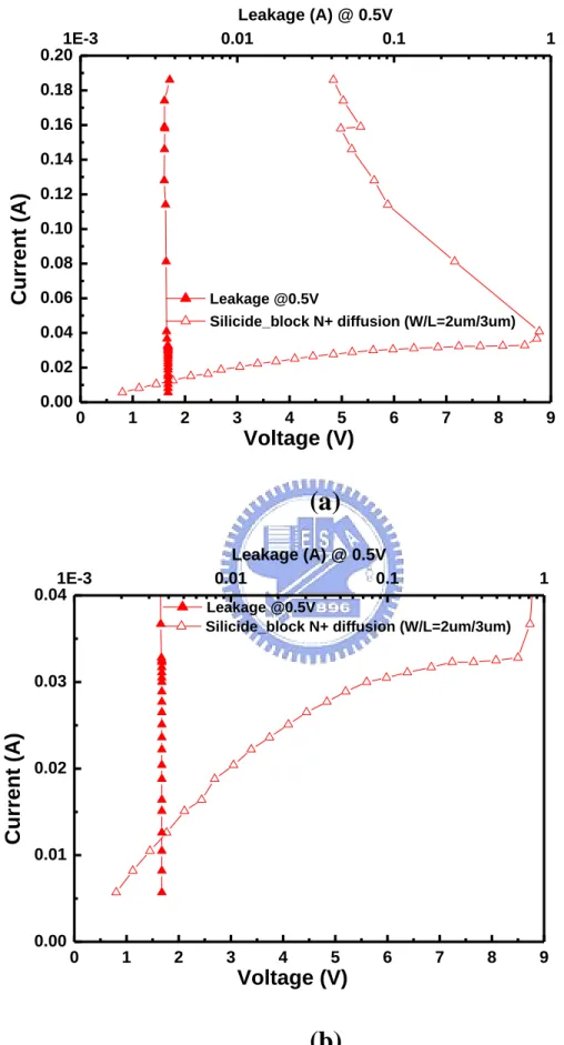
0.00 0.02 0.04 0.06 0.08 0.10 0.12 0.14 0.16 0.18 0.20 0 1 2 3 4 5 6 7 8 9 Leakage @0.5V
Silicide_block N+ diffusion (W/L=2um/3um)
C urre nt (A) Voltage (V) 1E-3 0.01 0.1 1 Leakage (A) @ 0.5V
(a)
0.00 0.01 0.02 0.03 0.04 0 1 2 3 4 5 6 7 8 9 Leakage @0.5VSilicide_block N+ diffusion (W/L=2um/3um)
C urre nt (A) Voltage (V) 1E-3 0.01 0.1 1 Leakage (A) @ 0.5V
(b)
Fig. 3.4 High current IV Characteristics of a RPO N+ diffusion resistor (a) from linear region to snapback region, (b) from linear region to saturation region.
0 1 2 3 4 5 6 7 8 9 10 1E-11 1E-10 1E-9 1E-8 1E-7 1E-6 1E-5 Cu rr en t (A ) Voltage (V) RPO N+/PW, BV 8.5V 0 1 2 3 4 5 6 7 8 9 10 1E-11 1E-10 1E-9 1E-8 1E-7 1E-6 1E-5 Cu rr en t (A ) Voltage (V) RPO N+/PW, BV 8.5V
0 50 100 150 0.0 0.5 1.0 1.5 2.0 Stress Voltage Stress Current
Time (ns)
Voltage (V) -5 0 5 10 15 20 Cur re nt ( mA )2L/V
stress
Reflect wave
Incident
wave
0 50 100 150 0.0 0.5 1.0 1.5 2.0 Stress Voltage Stress CurrentTime (ns)
Voltage (V) -5 0 5 10 15 20 Cur re nt ( mA )2L/V
stress
Reflect wave
Incident
wave
(a)
0 50 100 150 0 50 100 150 200 250 Power (VI) R (V/I)Time (ns)
Resistanc e (oh m) 0.000 0.005 0.010 0.015 0.020 0.025 0.030 Pow er (W)(a)
Fig. 3.6 Linear region:
(a) Voltage and Current waveforms, (b) Resistance (V/I) and power (V×I) vs. time for a RPO N+ diffusion resistor under the 100nsec TLP pulse event.
0 50 100 150 0 2 4 6 8
Time ( ns )
Vo
ltag
e (
V
)
Meas. V Theoretical V 0 10 20 30 40 50Cu
rre
nt
( m
A
)
Meas. I Theoretical Istress
0 50 100 150 0 2 4 6 8Time ( ns )
Vo
ltag
e (
V
)
Meas. V Theoretical V 0 10 20 30 40 50Cu
rre
nt
( m
A
)
Meas. I Theoretical Istress
stress
(a)
50 100 150 50 100 150 200 250Time ( ns )
R
es
is
atn
ce
(
oh
m
)
R based meas. V and I Theoretical R 0.0 0.1 0.2 0.3 0.4 0.5
P
ow
er (
W
)
Power based on meas. V and I
(b)
Fig. 3.7 Thermal region: (a) Voltage and Current waveforms, (b) Resistance (V/I) and power (V×I) vs. time for a RPO N+ diffusion resistor under the 100nsec TLP pulse event.
Rs(50
)
Vs
Vss
R(t)
TLP System
I(t)
V(t)
Rs(50
)
Vs
Vss
R(t)
TLP System
I(t)
V(t)
Fig. 3.8 Equivalent circuit of a RPO N+ diffusion resistor under the 100nsec TLP pulse event.
0 50 100 150 0 2 4 6 8
Time ( ns )
Vo
ltag
e ( V
)
Meas. V Theoretical V 0 10 20 30 40 50 60Cu
rrent
( m
A )
Meas. I Theoretical I(a)
0 50 100 150 50 100 150 200 250 300Time ( ns )
R
es
is
atn
ce
(
oh
m
)
R based on meas. V and I Theoretical R 0.0 0.1 0.2 0.3 0.4 0.5 0.6 0.7P
ow
er
(
W
)
Power based on meas. V and I
(b)
Fig. 3.9 Saturation region: (a) Voltage and Current waveforms, (b) Resistance (V/I) and power (V×I) vs. time for a RPO N+ diffusion resistor under the 100nsec TLP pulse event.
0 50 100 150 0 1 2 3 4 5 6 7 8 9 10
Voltage (V
)
C
urre
nt (mA
)
Time (ns)
Stress Voltage Stress Current 0 20 40 60 80 100 120stress
snapback
0 50 100 150 0 1 2 3 4 5 6 7 8 9 10Voltage (V
)
C
urre
nt (mA
)
Time (ns)
Stress Voltage Stress Current 0 20 40 60 80 100 120stress
snapback
(a)
0 50 100 150 50 100 150 200 250 R (V/I) Power (VI) 0.0 0.1 0.2 0.3 0.4 0.5 0.6 0.7 Pow er (W)Time (ns)
Re sista nce (ohm)snapback
0 50 100 150 50 100 150 200 250 R (V/I) Power (VI) 0.0 0.1 0.2 0.3 0.4 0.5 0.6 0.7 Pow er (W)Time (ns)
Re sista nce (ohm)snapback
(b)
Fig. 3.10 Snapback region: (a) Voltage and Current waveforms, (b) Resistance (V/I) and power (V×I) vs. time for a RPO N+ diffusion resistor under the 100nsec TLP pulse event.
(a)
(b)
Fig. 3.11 The current (a) before the snapback region, (b) at the snapback region.
0 50 100 150 0.0 0.5 1.0 1.5 2.0 2.5
Voltag
e(V)
Time(ns)
Substrate potentialsnapback
0 50 100 150 0.0 0.5 1.0 1.5 2.0 2.5Voltag
e(V)
Time(ns)
Substrate potentialsnapback
0.00 0.05 0.10 0.15 0.20 0.25 0.30 0 2 4 6 8 10 12 14 16 18 Leakage @0.5V Silicide N+ diffusion (W/L 2/16.5) Cu rr en t ( A ) Voltage (V) 0.01 0.1 1 10 100 1000 Leakage (A) @0.5V A (linear region) B (thermal region) C (saturation region) D (breakdown region) 0.00 0.05 0.10 0.15 0.20 0.25 0.30 0 2 4 6 8 10 12 14 16 18 Leakage @0.5V Silicide N+ diffusion (W/L 2/16.5) Cu rr en t ( A ) Voltage (V) 0.01 0.1 1 10 100 1000 Leakage (A) @0.5V A (linear region) B (thermal region) C (saturation region) D (breakdown region)
(a)
0.00 0.02 0.04 0.06 0.08 0.10 0.12 0.14 0.16 0 2 4 6 8 10 12 14 Leakage @0.5V Silicided N+ diffusion (W/L 2/16.5) Cu rr e n t ( A ) Voltage (V) 0.01 0.1 1 10 100 1000 Leakage (A) @0.5V A (linear region) B (thermal region) C (saturation region) 0.00 0.02 0.04 0.06 0.08 0.10 0.12 0.14 0.16 0 2 4 6 8 10 12 14 Leakage @0.5V Silicided N+ diffusion (W/L 2/16.5) Cu rr e n t ( A ) Voltage (V) 0.01 0.1 1 10 100 1000 Leakage (A) @0.5V A (linear region) B (thermal region) C (saturation region)(b)
Fig. 3.13 (a) High current IV Characteristics of a Silicided N+ diffusion resistor, (b) Zoom-In.
39
(a)
0 50 100 150 0 10 20 30 40 50 Resis tan ce ( o h m ) P o w er ( W) R (V/I) Power (VI)Time (nsec)
0.000 0.005 0.010 0.015 0.020 0.025 0.030 0.5 1.0 1.5 2.0 Stress Voltage Stress CurrentV
o
lt
a
g
e
(
V
)
5 10 15 20C
u
rr
e
n
t (
m
A
)
0 50 100 150 0 10 20 30 40 50 Resis tan ce ( o h m ) P o w er ( W) R (V/I) Power (VI)Time (nsec)
0.000 0.005 0.010 0.015 0.020 0.025 0.030 0.5 1.0 1.5 2.0 Stress Voltage Stress CurrentV
o
lt
a
g
e
(
V
)
5 10 15 20C
u
rr
e
n
t (
m
A
)
(b)
Fig. 3.14 Linear region:
(a) Voltage and Current waveforms, (b) Resistance (V/I) and power (V×I) vs. time for a silicided N+ diffusion resistor under the 100ns pulse event.
0 50 100 150 0 1 2 3 4 5 6 V o ltag e (V ) Cur ren t ( m A )
Time (nsec)
Stress Current Stress Voltage 0 20 40 60 80 100stress
0 50 100 150 0 1 2 3 4 5 6 V o ltag e (V ) Cur ren t ( m A )Time (nsec)
Stress Current Stress Voltage 0 20 40 60 80 100stress
0 50 100 150 0.0 0.5 1.0 1.5 2.0 Stress Voltage Stress CurrentTime (ns)
V o lt a g e ( V ) 0 5 10 15 20 C u rr e n t ( m A ) 0 50 100 150 0 1 2 3 4 5 6 V o ltag e (V ) Cur ren t ( m A )Time (nsec)
Stress Current Stress Voltage 0 20 40 60 80 100stress
0 50 100 150 0 1 2 3 4 5 6 V o ltag e (V ) Cur ren t ( m A )Time (nsec)
Stress Current Stress Voltage 0 20 40 60 80 100stress
0 50 100 150 0.0 0.5 1.0 1.5 2.0 Stress Voltage Stress CurrentTime (ns)
V o lt a g e ( V ) 0 5 10 15 20 C u rr e n t ( m A )(a)
0 50 100 150 35 40 45 50 55 60 Power (VI)Re
si
sa
tn
ce
(
o
h
m
)
Time ( ns )
R (V/I) 0.2 0.3 0.4 0.5 0.6Po
w
er
( W )
(b)
Fig. 3.15 Thermal region: (a) Voltage and Current waveforms, (b) Resistance (V/I) and power (V×I) vs. time for a silicided N+ diffusion resistor under the 100nsec TLP pulse event.