電子物理學系
博士論文
氮化矽的氫與其應力對電晶體之影響
Impacts of Hydrogen and Stress Of the
Silicon Nitride on the Transistors
研 究 生 :廖家駿
指導教授 :趙天生 博士
Impacts of Hydrogen and Stress Of the
Silicon Nitride on the Transistors
指導教授 : 趙天生 博士 Advisor : Dr. Tien-Sheng Chao
研 究 生 : 廖家駿 Student : Chia-Chun Liao
國立交通大學
電子物理學系
博士論文
A Dissertation
Submitted to Department of Electrophysics
College of Science
National Chiao Tung University
in Partial Fulfillment of the Requirements
for the Degree of Doctor of Philosophy
in Electrophysics
July 2011
Hsinchu, Taiwan, Republic of China.
中華民國 一百年 三月
氮化矽的氫與其應力對電晶體之影響
指導教授 : 趙天生 博士 研 究 生 : 廖家駿 國立交通大學 電子物理學系 摘要 首先,此研究確認了利用壓縮應力的氮化矽覆蓋層相較於伸張應力的氮化矽 覆蓋層具有較高於 N 型金氧半場效電晶體耦合應力記憶技術的潛力。我們提出 選用覆蓋層的方法應該被調整為使用應力改變量最大而非傳統挑選的初始應力 最大的覆蓋層。並且,我們也發現到初始覆蓋層內的氫含量與隨後於退火時釋放 的氫含量都會影響介面處懸浮鍵的鈍化。另一方面,退火後的應力而非應力改變 量主導了閘極氧化層的劣化,進而導致劣化的閘極漏電流,在熱載子的加壓測試 下顯現較高的臨限電壓位移,以及較差的閃爍雜訊。隨後,我們有系統的研究了 不同反應氣體流量所沉積的氮化矽對複晶矽薄膜電晶體的鈍化效應。覆蓋了氮化 矽的複晶矽薄膜電晶體能夠展現更佳的性能表現,壓抑電流突增效應(Kink effect) 與改善閘極漏電流與閘極導致的汲極漏電流(DIBL)。由於不同的鈍化效應,覆蓋 不同製程製備的氮化矽的原件會展現不同的效應。一物理機制被提出以解釋不完 整的缺陷鈍化所導致的雙駝(double hump)現象。根據不同寬度的元件比較,不只 是自由基在複晶矽內的缺陷鈍化作用會改善原件傳輸特性,閘極氧化層內的缺陷 鈍化也會造成元件特性的改善。此外,覆蓋了氮化矽的原件,會提升對於正閘極 電壓加壓測試,負閘極電壓加壓測試,與熱載子的加壓測試的免疫力。再者,此 製程非常的簡單(不需要面臨電漿處理需要長時間問題)並且與傳統薄膜電晶體 有很高的相容性。 隨後,此研究根據不同氮化矽厚度與不同的四乙氧基矽烷氧化層厚度討論了 富含氫的氮化矽對於氫鈍化效率的議題,並得到了利用氮化矽是十分有效率的鈍 化方法結論。氫會遭受隨後的退火製程導致的不穩定性也被詳細討論。結果顯示 使用氮化矽覆蓋層可以避免氫從複晶矽通道中釋放。然而,移除氮化矽會使得氫 在隨後的熱製程中釋放,而使得原件特性與對照樣本的特性相似。移除了氮化矽 的樣本可以減緩對於熱載子的加壓測試的劣化。然而,氫釋放會劣化對於正偏壓溫度不穩定性加壓測試與負偏壓溫度不穩定性加壓測試的免疫力。兩種可能的機 制被提出以解釋源自於氫釋放所導致的缺陷密度上升。此種不理想效應會影響熱 載子的加壓測試,正偏壓溫度不穩定性加壓測試與負偏壓溫度不穩定性加壓測 試。 最後,此研究討論了鄰近的薄膜對固相結晶與金屬側向結晶的影響。對於利 用固相結晶的原件來說,將元件製備在氮化矽薄膜上會改變臨限電壓對溫度的相 依性,其歸因於氫導致的成核點形成與氫或氮鈍化缺陷的行為。我們也發現在結 晶前移除晶背後的非晶矽會影響原件的表現,其歸因於應力的影響。對於利用金 屬側向結晶的原件來說,這些鄰近的薄膜不單會改變金屬側向結晶的速率,其也 會改變電特性,故硬遮罩,緩衝氧化層,與絕緣墊片會因為不同的結晶特性而影 響電特性。我們提出了三種可能的機制,包含了鎳捕捉,本質應力,與氫的參與, 以釐清臨近薄膜的影響。
Impacts of Hydrogen and Stress Of the
Silicon Nitride on the Transistors
Advisors:Dr. Tien-Sheng Chao Student:Chia-Chun Liao
Department of Electrophysics National Chiao Tung University
Abstract
First, this dissertation certified that the compressive SiN capping layer has more potential than the tensile layer for fabrication using the stress memorization technique to enhance NMOS mobility. The mechanism that we have proposed implies that the conventional choice of the capping layer should be modulated from the point of view of the stress shift rather than using the highest tensile film. We also found that both the initial component of the deposited capping layer and the H released during annealing affected interface-state passivation. On the other hand, the annealed stress rather than the stress shift are responsible for degraded gate oxide quality, leading to the degraded gate leakage, higher threshold voltage shift under hot carrier stressing, and degraded flicker noise. Then, the effect of the flow rate of different reactant gases on the deposition of the SiN layer for passivation of poly-Si TFTs had systematically investigated. SiN passivation layers were found to yield better performance, suppress the kink effect, and improve the gate leakage current and gate induce drain leakage (GIDL) of polysilicon thin film transistors (poly-Si TFTs). The SiN passivation layers deposited under different deposition conditions possess different characteristics, due to their varying passivation effect. A physical mechanism is proposed to explain the double hump phenomenon induced by incomplete trap passivation. Based on the analysis of width dependence, the better performance of the samples with SiN passivation layers was attributed to not only the radical passivation of the defect states, but also the radical passivation of pre-existing defects in the gate oxide. Furthermore, using SiN passivation layers improves the immunity to positive gate bias stress, negative gate bias stress, and hot carrier stressing. Moreover, the manufacturing processes are simple (without the long processing time plasma treatment requires) and compatible with TFT processes.
hydrogen-containing nitride, based on a comparison of different thicknesses of SiN or inserted TEOS oxide, indicating that hydrogen diffusion is efficient. Hydrogen instability induced by post annealing is also reviewed in detail. Results show that using a SiN capping layer can prevent the release of hydrogen from a poly-Si channel. However, removing this SiN capping layer allows the hydrogen release during post annealing, and the resulting device performance becomes comparable to the control sample. Samples with SiN capping layers removed can alleviate degradation by hot carrier stressing. However, hydrogen release reduces the immunity of PBTI and NBTI. Two possible mechanisms can explain the increased pre-existing defects associated with hydrogen release, which affects the hot carrier stressing, NBTI, and PBTI.
Finally, this dissertation presented the impacts of the proximity layer on the SPC and MILC. For samples crystallized by SPC, the temperature dependence of threshold voltage are different for samples fabricated on the SiN proximity layer, and the formation of seed nuclei by hydrogen or traps passivated by hydrogen and nitrogen are responsible for this temperature dependence. Also, we found that removal of the backside a-Si before the crystallization would alter the performance originating from the stress viewpoint. For samples crystallized by MILC, The proximity layers not only affect the MILC growth rate, but also the electrical characteristics, meaning that the materials of the hard mask, the buffered layer, and the spacer affect the electrical characteristics due to the different crystallization conditions. Based on the comparison among the proximity layers, the SiN proximity layer is not suitable to be a hard mask or a spacer, due to the concern of crystallization condition. We proposed three reasonable mechanisms, including the gettering of Ni, the intrinsic stress, and the involvement of hydrogen, to make the deep understanding of the impacts of proximity layers.
誌 謝 四年多的時間,由當初的懵懵懂懂的大學生逐漸成長為競競業業的博士生, 這條路對於不聰慧的我來說顯得並不容易。感謝趙天生老師對我生活上與學術上 的提攜與指導,讓學生在面對挫折時更有韌性,面對挑戰時更有熱情。謝謝老師 給了我很多機會在這四年中嘗試新的挑戰,並讓我在獲得知識的同時,也學會謙 卑。在交大求學的日子裡,能受到老師的關愛與培養,真的是很幸福的事。 衷心感謝指導過我的建豪學長(現在用不到的知識不代表以後用不到),偉成 學長(要鑽研一樣知識最少要理解完一百篇研究),與小馬學長(每學期全力修一門 課而不要旁聽),你們的一字一句,讓我的博生班少走了很多彎路。感謝德馨學 長、文政學長與宗宜學長,讓我的求職之路不會徬徨無助。感謝宗裕,哲偉與冠 迪,在我覺得自己快走不下去時,你們總適時的伸出援手~拯救快溺斃的我。感 謝郭柏儀學長、阿壘、翊鴻、佑倫、智盟、高興、啟瑞、士安、小喬、pebble、 小聿、阿昌、肉肉、阿堂、添舜、立盈、芳昌、其儒、明慈、小紅、哲毅、大鈞、 樂樂、小小、偉斌、與貽泓,陪我吃喝玩樂以及培養勇健的體魄。 謝謝我帶過的學弟妹,岷臻、小劉,與儀儒,給我這個機會與你們一起研究 學問。很多實驗沒有你們的耐心以及包容我的任性與高標準,勢必是無法如期成 功完成的,不管是熬夜的收爐管、龜毛的換酸、惱人的電漿、假日量測的犧牲、 以及相關資料的查詢,真的幸好有你們,也真的~辛苦了。 要感謝的還有一群在求學旅途上的朋友,彩雲、豬頭、厚勇、瑞洋、永誠、 麒麟、小悶、與大柄老師,沒有你們的鼓勵與陪伴,我想我不會有足夠的勇氣踏 上追求學問這條路,品味不同的生活,嘗試不同的人生。 謝謝屁精、阿嬤、boss、泡麵、董龜、自清、怡君、智盈、清翔、立辰、愈 帆、與所有武陵高中 309 的同學們,一起拚命為了理想努力,一起品嘗青春的酸 甜苦辣。有了你們與我在人生的旅途上互相扶持,以及互相激盪碰撞出新的火花, 我才了解到什麼叫青春與快樂;每當我覺得自己喘不過氣時,幸好有你們這罐永 不過期的氧氣 ~ 讓我能大口呼吸。跟你們相處的日子,是我最輕鬆快樂的時光, 也是我最珍惜的回憶。 謝謝小區、sherry、阿海與 Joanne,讓我鼓起勇氣簽下博士班這個賭注,並 讓我的視野更寬廣更開闊,更了解自己除了在半導體的知識外,仍有許多不足的 地方需要加強,並對未完成的夢想,持續燃燒熊熊的熱情與希望。世界比我想像 的更大,而我該勇敢鼓動翅膀,勇敢往未知的地方翱翔。 感謝室友:吉米、長新、昌恩、牧民、崧宏、家群、與青宇。在我遭受挫折 時,你們的即時救援就像是充滿元氣的大補丸。總讓我能在跌倒後,迅速的復原 並克服挑戰。這條路上充滿著跌跌撞撞~幸好總有你們相知與相伴。 感恩最好的兩個知己,凱齡與希文,謝謝你們在這輩子願意來到我身邊,了 解我、懂我、並照顧我。陪我分擔風雨中的苦與悲,分享生命中的酸與甜。因為 擁有你們,我才能在挫折中,學會堅強,變的茁壯。此份得來不易的學術成就, 是屬於我們三個人的榮耀。 最後,謹以此本博士論文,獻給我的爸媽,廖振山先生與劉梅香女士,沒有 你們無私的關懷與愛,就不會有今日的我。感謝你們在我每一個人生的交岔口, 願意停下來等等我,為我點起一盞盞的燈指引方向,你們是我這輩子最大的寶藏 ~這輩子能夠當你們的兒子,我覺得很幸福。
2012 于 風城∙交大
Contents
Abstract (Chinese)………...………...….…...I Abstract (English)……….…………...……...…...III Acknowledgement (Chinese)………...………...…..….V Contents……….…...………...………....VI Table Caption……….………..…..……...IX Figure Caption……….………..…………....……...XChapter 1 Introduction
1.1 Background……….………….... 1 1.2 Motivation……….………..… 71.3 Organization of the Dissertation………..………….………... 9
Chapter 2 Stress of SiN and Stress Memorization in Devices.
2.1 Introduction……….……. 152.2 Experiment……….... 16
2.2.1 Material Analysis………16
2.2.2 Device Fabrication……….18
2.3 Results and Discussions………... 19
2.3.1 Device Performance……….………. 19
2.3.2 Hot Carrier Stress……….. 23
2.3.3 Flicker Noise……….…..24
2.4 Summary……….... ...26
Chapter 3 Effects of Channel Width and Nitride Passivation Layer
on Electrical Characteristics of Polysilicon Thin-Film Transistors
3.1 Introduction………..… 473.2 Experiment……….... 48
3.3 Results and Discussions………....………... 49
3.3.1 Performance………... 49
3.3.2 Width Dependence of TFT Capped Nitride Passivation Layers……….. 51
3.3.4 Post-SiN-deposition Thermal Annealing………...54
3.4 Summary………...……....….... 55
Chapter 4 Hydrogen Instability Induced by Post Annealing on
Poly-Si TFTs
4.1 Introduction………...664.2 Experiment……….67
4.3 Results and Discussions……….……….……. 67
4.3.1 Thickness Control of Deposited Inserted TEOS oxide and SiN films...67
4.3.2 Hydrogen Instability Induced by Post Annealing…….……… …...69
4.3.3 Hot Carrier Stressing, PBTI, and NBTI………....70
4.4 Summary ………..………..………..…….... 72
Chapter 5 Impacts of the Underlying Insulating Layer on the SPC
and MILC.
5.1 Introduction………...875.2 Experiment 5.2.1 Device Fabricated by SPC………..88
5.2.2 Device Fabricated by MILC………...88
5.3 Results and Discussions 5.3.1 Impacts of SiN and Backside Amorphous Silicon on Poly-Si TFTs……89
5.3.2 Impacts of Underlying Insulating layer on the MILC Growth Length and Electrical Characteristics………91
5.4 Summary………93
Chapter 6 Conclusions and Recommendations for Future Research
6.1 Conclusions………..…. ..1065.2 Recommendations for Future Research……….. ..108
Publication List
………..………..……….………..…... 135Table Captions
Chapter 2
Table 2.1 Properties of all nitride samples. ………. 27 Table 2.2 Characteristics of value with different gate voltage for all samples...44
Chapter 3
Table 4.1 Properties of all nitride splits. ……….. 65
Chapter 5
Figure Captions
Chapter 1
Fig. 1.1 2010 ITRS Process integration Devices and structures Logic potential
solution ………...…. 11
Fig. 1.2 (a) Si capped on SiGe substrate can possess biaxial strain property. (b) Contact etch stop layer induce uni-axial stain....………..11
Fig. 1.3 (a) SiGe S/D possessed larger lattice constant induces compressive uni-axial strain laterally into the channel (b) SiC S/D possessed smaller lattice constant induces tensile uni-axial strain laterally into the channel. (c) The poly gate thermal volume expansion induces strain memorization for SMT applications………...………... 12
Fig. 1.4 Silicon without strain coupling possesses six- fold degenerate valley...…13
Fig. 1.5 With biaxial strain coupling, the carrier would redistribute into ∆2 valley...13
Fig. 1.6 With <110> uni-axial strain coupling , the carrier would redistribute into ∆2 valley………...….14
Fig. 1.7 With <100> uni-axial strain coupling, the E-k relation would transfer into an anisotropic occupation of four fold valley...………..14
Chapter 2
Fig. 2.1 (a) Influence of N2 flux on N/Si atomic ratio. (b) Influence of SiH4 flux on N/Si atomic ratio.……….28Fig. 2.2 Characteristics of XPS for all initial and annealed SiNx...29
Fig. 2.3 The Si-N Characteristics of FTIR for all samples before annealing...30
Fig. 2.4 The Si-N Characteristics of FTIR for all samples after annealing. ...30
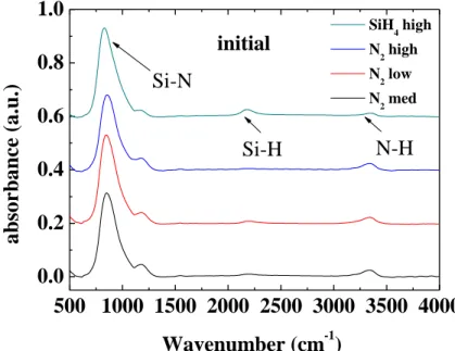
Fig. 2.5 Initial FTIR of N2 rich, N2 med, N2 low, SiH4 rich, and control sample for analyzing the H content. ...31
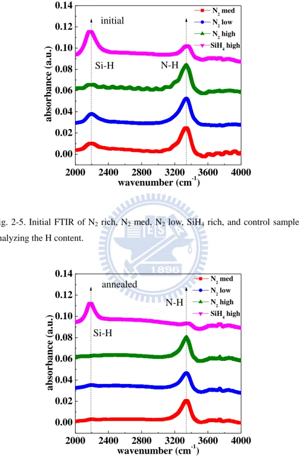
Fig. 2.6 Annealed FTIR of N2 rich, N2 med, N2 low, SiH4 rich, and control sample for analyzing the H content. ...31
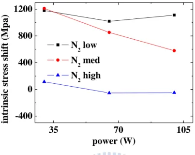
Fig. 2.7 The connection between initial intrinsic stress and power for N2 low, N2 med, and N2 high. ...32
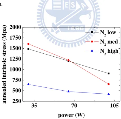
Fig. 2.8 The connection between intrinsic stress after annealing and power for N2
low, N2 med, and N2 high. ...32
Fig. 2.9 The connection between intrinsic stress shift after annealing and power for N2 low, N2 med, and N2 high. ...33
Fig. 2.10 Intrinsic stress characteristics as N2 low for Once-deposition,
Multi-deposition, and Implant treatment. ...33
Fig. 2.11 Intrinsic stress characteristics as SiH4 low for Once-deposition,
Multi-deposition, and Implant treatment. ...34
Fig. 2.12 Gm/Cinv for NMOSFET with different capping layer SiN (1500Å ) in linear
region with channel length equal to 0.4μm. ...34
Fig. 2.13 Initial strain, after annealing strain, and the strain shift by annealing process of different N2 and SiH4 flux. ...35
Fig. 2.14 The traditional thermal poly-Si expansion mechanism. ...35 Fig. 2.15 The new model with the mechanically induced strain mechanism for the
capping layer. ...36 Fig. 2.16 Id-Vg for different SiN at Vg=0.05V characteristics. The inset shows the
subthreshold swing for different SiN. ...36 Fig. 2.17 Charge pumping analysis of all strain samples and the control sample with
frequency of 2 MHz and voltage amplitude 1V. ...37 Fig. 2.18 The connection between intrinsic stress shift and charge pumping
current...37 Fig. 2.19 Gm/Cinv for NMOSFET with silicon gate (2000Å ) with different deposition
temperature in linear region with channel length equal to 0.4μm...38 Fig. 2.20 Charge pumping analysis of strain samples by different deposition
temperature with frequency of 2 MHz and voltage amplitude 1V. ...38 Fig. 2.21 Characteristics of gate leakage were investigated. All strain samples possess
Fig. 2.22 Stress of all capping layers sketched as initial stress and annealed stress in order of magnitude. ...39 Fig. 2.23 Substrate current versus gate voltage for all samples with device size
W/L=10μ /0.35μ . ...40 Fig. 2.24 Threshold Voltage shift as a function of stress time. Devices with
W/L=10μ /0.35 μ were stressed at , and of maximum substrate current. ...40 Fig. 2.25 Charge pumping current with W/L=10μ /0.35μ before and after 5000sec
hot carrier stressing for all samples. ...41 Fig. 2.26 Charge pumping current shift as a function of stress time. Devices with
W/L=10μ /0.35 μ were stressed at , and of maximum substrate current. ...41 Fig. 2.27 Transconductance degradation as a function of stress time. Devices with
W/L=10 /0.35 were stressed at , and of maximum
substrate current. ...42 Fig. 2.28 Charge pumping current characteristics as a function of stress time. Devices
with W/L=10μ /0.35μ were stressed at , and of maximum substrate current. ...42 Fig. 2.29 Schematic illustration of electrons in the channel of NMOS moving in and
out of traps, giving rise to fluctuations in the inversion charge density and drain current consequently. ...43 Fig. 2.30 Schematic setup for flicker noise measurement. ...43 Fig. 2.31 Input-referred gate voltage noise spectral density (SVg) as a function of gate
voltage at Vd=0.05V and f=25Hz. ...44
Fig. 2.32 SVg@25 Hz for all samples under Vg-Vth=0.87V and Vd=0.05V...45
Fig. 2.33 Hydrogen diffuses and passivates the interface state, improving low frequency noise. However, if nitride stress reaches a detrimental level during annealing, it degrades oxide quality and flicker noise behavior. ...45 Fig. 2.34 Band diagram indicating the tunneling transitions of electrons between
conduction band and traps in the gate oxide, (a) direct tunneling and (b) indirect tunneling via interface traps...46
Chapter 3
Fig. 3.1 Transfer characteristics (ID-VG) of n-channel TFTs with different
passivation layers. ...56 Fig. 3.2 Transconductance of n-channel TFTs with different passivation layers. ....56 Fig. 3.3 Output characteristics (the ID-VD curve) of n-channel TFTs with different
passivation layers. ...57 Fig. 3.4 Gate leakage current of n-channel TFTs for all samples. ...57 Fig. 3.5 Transfer characteristics (ID-VG) for N2-high sample with different channel
width. ...58 Fig. 3.6 (a) Cross-section of n-channel TFTs with wider channel widths. The
incomplete trap passivation is also indicated, and is responsible for the double hump phenomenon. ...58 Fig. 3.6 (b) Cross-section of n-channel TFTs with narrower channel widths. The
complete trap passivation appears to suppress the double hump phenomenon. ...59 Fig. 3.7 (a) Variation of subthreshold swing as a function of channel width for
L 10 with different passivation layers. ...59 Fig. 3.7 (b) Variation of threshold voltage as a function of channel width for
L 10μ with different passivation layers. ...60 Fig. 3.7 (c) Variation of field mobility as a function of channel width for L 10μ with different passivation layers. ...60 Fig. 3.8 Threshold voltage shift as a function of stress time for n-channel TFTs under positive gate bias stress as VGS =11V ...61
Fig. 3.9 Threshold voltage shift as a function of stress time for n-channel TFTs under negative gate bias stress as VGS= -10V...61
Fig. 3.10 (a) Dependence of Ion degradation under dc stress on gate voltage for all
samples. ...62 Fig. 3.10 (b) Dependence of Vth degradation under dc stress on gate voltage for all
Fig. 3.10 (c) Dependence of transconductance degradation under dc stress on gate voltage for all samples. ...63 Fig. 3.11 Transfer characteristics (ID-VG) of n-channel TFTs with different
passivation layers after the post annealing. ...63 Fig. 3.12 Transconductance of n-channel TFTs with different passivation layers after
the post annealing. ...64 Fig. 3.13 A mechanism of hydrogen instability induced by post annealing. ...64
Chapter 4
Fig. 4.1 Process flow and split table...74 Fig. 4.2 Schematic diagram of three types of deposition process for TEOS oxide or
SiN based on the same thermal budget. ...75 Fig. 4.3 (a) Variation of threshold voltage as a function of channel width for sample
with L 10μ capped thickness of SiN capping. Fig. 4-3(b) Variation of threshold voltage as a function of channel length for sample with W 10μ capped different thickness of SiN capping. ...76 Fig. 4.4 (a) Variation of mobility as a function of channel width for sample with L 10μ capped different thickness of SiN capping. Fig. 4-4(b) Variation of mobility as a function of channel length for sample with W 10μ capped different thickness of SiN capping. ...77 Fig. 4.5 (a) Variation of threshold voltage as a function of channel width for sample
withL 10μ capped different thickness of TEOS oxide capping. Fig. 4-5(b) Variation of threshold voltage as a function of channel length for sample with W 10μ capped different thickness of TEOS oxide capping. ...78 Fig. 4.6 (a) Variation of mobility as a function of channel width for sample with
L 10μ capped different thickness of TEOS oxide capping. Fig. 4-6(b) Variation of mobility as a function of channel length for sample with W 10μ capped different thickness of TEOS oxide capping...79 Fig. 4.7 (a) Variation of threshold voltage as a function of channel width with
L 10μ for the control sample, the nitride capped sample, and the nitride removed sample. Fig. 4-7(b) Variation of threshold voltage as a function of
channel length with W 10μ for the control sample, the nitride capped sample, and the nitride removed sample. ...80 Fig. 4.8 Fig. 4-8(a) Variation of mobility as a function of channel width with
L 10μ for the control sample, the nitride capped sample, and the nitride removed sample. Fig. 4-8(b) Variation of mobility as a function of channel length with W 10μ for the control sample, the nitride capped sample, and the nitride removed sample. ...81 Fig. 4.9 Output characteristics (the ID-VD curve) of n-channel TFTs with W/L
10μ /10μ for the control sample, the nitride capped sample, and the nitride removed sample. ...82 Fig. 4.10 (a) The minimum current for the control sample, the nitride capped sample, and the nitride removed sample. Fig. 4-10(b) The gate voltage corresponding to minimum leakage current at fixed drain bias for the control sample, the nitride capped sample, and the nitride removed sample. ...83 Fig. 4.11 The activation energies of the drain current for the control sample, the nitride capped sample, and the nitride removed sample. ...84 Fig. 4.12 Dependence of Ion and Gm degradation under dc stress on gate voltage for
the control sample, the nitride capped sample, and the nitride removed sample. ...84 Fig. 4.13 Threshold voltage shift as a function of stress time for the control sample,
the nitride capped sample, and the nitride removed sample with W/L 10μ /10μ under positive gate bias stress as 19 . ...85 Fig. 4.14 Threshold voltage shift as a function of stress time for the control sample,
the nitride capped sample, and the nitride removed sample with W/L 10μ /10μ under negative gate bias stress as −19 . ...85 Fig. 4.15 Measurement of NBTI degradation at different temperatures for the control
sample, the nitride capped sample, and the nitride removed sample with W/L 10μ /10μ . ...86
Chapter 5
Fig. 5-1 Schematic of the proposed process...94 Fig. 5-2 Schematic diagram of MILC process. ...95
Fig. 5-3 Residual stress change in amorphous silicon thin film. ...96 Fig. 5-4 Threshold voltage for samples deposited on oxidized wafers. ...97 Fig. 5-5 The mechanism of the stress impacts induced by backside amorphous silicon...97 Fig. 5-6 Threshold voltage for samples deposited on oxidized wafers with inserted SiN. ...98 Fig. 5-7 Output characteristics of samples deposited on on oxidized wafers. ...98 Fig. 5-8 ∆ FB as a function of time for control sample stressed by different electric field. ...99 Fig. 5-9 ∆ FB as a function of time for samples with and without removing back side layer. ...99 Fig. 5-10 The gate voltage corresponding to minimum leakage current at fixed drain bias for samples deposited on oxidized wafers. ...100 Fig. 5-11 The minimum current of samples deposited on oxidized wafers at different VD. ...100
Fig. 5-12 The minimum current of samples deposited on oxidized wafers with inserted SiN at different VD. ...101
Fig. 5-13 The dependence of the MILC length on the underlying insulating layers...102 Fig. 5-14 The FTIR of Wet Oxide, TEOS oxide, and SiN for analyzing the H content. ...102 Fig. 5-15 Transfer characteristics (ID-VG) of p-channel TFTs with different underlying
insulating layers. ...103 Fig. 5-16 Variation of threshold voltage as a function of channel width for W/L 10μ /10μ . The inset shows the Variation of subthreshold swing as a function of channel width for W/L 10μ /10μ . ...104 Fig. 5-17 Variation of mobility as a function of channel width for W/L 10μ / 10μ . ...104 Fig. 5-18Output characteristics (the ID-VD curve) of n-channel TFTs with W/L
Chapter 1
Introduction
1.1 Background
SiN is one of the promising materials for sealing substrate against the process chemical, the outstanding adhesion, and the application of the gate dielectric or FinFET fabrication [1.1]-[1.3]. Recently, the interest in studying the capabilities of devices capped silicon nitride has been rapidly growing, including the potential of the strain coupling for metal-oxide-semiconductor field-effect transistors (MOSFETs) and the trap passivation by hydrogen radicals for poly-Si thin film transistors.
1.1.1 Strained Channel Technology
Strain techniques has emerged as one of the most promising remedies for boosting the drive current in scaled devices since 1980s [1.4]-[1.5]. When the band structure of material is changed by strain, the band gap, mobility, effective mass, diffusivity of dopants, and oxidation rate is altered simultaneously. The stress induced by local oxidation of silicon and shallow trench isolation was investigated about the impact on electron and hole mobility since 1997. However, the strain from a localized source decays rapidly away from the booster, it was not until deep submicrometer technologies were developed that these effects were observed experimentally [1.6]. For no significant processing cost, the mobility advantage offered by strain technology is a promising technique to meet transistor target as Fig.1-1 [1.7]. The strained thin film Si or Ge capped on strain-relaxed SiGex buffer (SRB) as Fig. 1-2 (a)
can create bi-axial tensile or compressive stress, and the mobility of carrier could be enhanced significantly. Whether or not SRB layer is used underneath will make influence on both misfit and threading dislocations [1.8]. Both electron and hole mobility are enhanced by tensile strain induced in the thin epitaxial Si layer grown on
a relaxed SiGe virtual substrate [1.9]. It is noted that the capping film should be optimized to control the underlying relaxed SiGe layer dislocation penetration and Ge out-diffusion during annealing, or the damaged interface state, gate oxide quality, and even bulk substrate trap would severely degrade device performance, reliability and flick noise characteristics [1.10]-[1.11]. Besides, the high wafer cost and enhancement loss at high vertical field possess significant concern [1.12]. In the 1990s, anther strained channel technology was proposes, uni-axial strain, which is induced by process and free from the aforementioned concerns of bi-axial strain. Compared to biaxial technique, uni-axial strain provides larger enhancement at both low strain and high vertical electric field due to difference in the warping of the valence band.
Uni-axial strain was thoroughly investigated by a large number researcher. Contact etching stop layer (CESL) was employed to generate uni-axial strain as Fig. 1-2(b) [1.13]-[1.16]. This technique can be easily incorporated into conventional process. Depending on the SiN fabrication process, the SiN could possess tensile stress or compressive stress. Dual-SiN stressor could both enhance NMOS and PMOS performance with appropriate CESL adoption, respectively.
The embedded SiGe source drain was adopted for PMOS, and the channel region would meet compressive strain by SiGe S/D stress as Fig. 1-3(a) [1.17]-[1.18]. Thus, the mobility of hole and drive current would enhance. Subsequently, the Si1-yCy
(y=1~2%) was proposed to fabricate tensile strain to promote NMOS performance as Fig. 1-3(b) [1.19]-[1.20]. Although the Ge-outdiffusion is avoided, C precipitation and C-related interface state are a crucial issue.
Recently, stress memorization technique (SMT) was introduced as a promising technique [1-21]-[1.25]. By the capping layer such as SiN or TEOS oxide and spacer confinement, the expanded volume of poly silicon gate would release its volume downward during annealing, and make the channel become vertical compressive as
Fig. 1-3(c). It is noted that the vertically compressive could significantly enhance electron mobility. Since the strain would enter plastic regime, the strain would remain after the capping layer was removed. Besides, the phenomenon of material expansion also plays a critical role in the SMT process. For poly-Si implantation, the deeper the Rp projection range using the same dosage, the more obvious the stress memorization.
More effective recrystallization would thus occur and the volume swelling could be enhanced significantly.
1.1.2 Polysilicon TFT
Polycrystalline silicon thin-film transistors (poly-Si TFTs) have been studied because of their potential application in high performance active matrix thin-film displays on glass substrates and high density vertically components [1.26]. The polysilicon layer is a disordered material with a significant number of defect states. This high density of defects would degrade threshold voltage, subthreshold swing, mobility, and leakage current.
Because the grain boundaries in poly-Si TFTs have a profound influence on device characteristics and degrade carrier transport, developing promising techniques to reduce the trap density is important. Poly-Si has been formed using a variety of techniques, such as direct growth by low-pressure chemical vapor deposition (LPCVD) [1.27], and annealing of amorphous silicon (a-Si) by rapid thermal annealing (RTA) [1.28], laser crystallization (LC) [1.29], and solid-phase crystallization (SPC) [1.30]. Also, Nickel (Ni) based metal-induced lateral crystallization (MILC) of a-Si has been proposed to obtain high performance TFTs. RTA is a high temperature ( >600oC) process, resulting in films with a high defect density [1.31]. By localizing the high temperature to the silicon film, LC can be
considered a “low-T” process. Although it is capable of producing poly-Si films with low defect density, is suffers from high initial setup cost, high process complexity, and unacceptable uniformity. Conventional SPC possesses a relatively inexpensive batch process and a superior uniformity, the process temperature is still high. Moreover, MILC process would encounter the issue of metal residue, leading to unacceptable leakage current [1.32].
Previous research shows that hydrogen plasma treatment and hydrogen-containing nitride film deposition are promising approaches for improving performance [1.33]- [1.35], because hydrogen radicals can effectively passivate the defects of intra-grain, grain boundary, and the gate dielectric [1.33]- [1.34]. Also, O2,
N2 and CF4 plasma have also been found to be effective to enhance the poly-Si TFTs
performance [1.35]- [1.37].
Using the non-hydrostatic stress is another approach for improving the poly-Si TFT performance. A lot of works have been done for clarifying the influence of the mechanical stress, including the stress applied before the crystallization [1.38] or after the crystallization [1.39]. For the stress applied before the crystallization, the tensile stress increases the growth rate of the crystallization, but the compressive stress retards the growth rate of the crystallization. For the stress applied after the crystallization, the tensile stress would increase the electron mobility, but degrade the hole mobility.
1.1.3 Mobility Enhancement Physics
The carrier mobility is given by , where is the mean free time and m* is the conductivity effective mass. With the strain coupling, the changed band
structure of Silicon modulates inter-valley scattering probability as well as effective mass. For NMOS, electron distribute in the six degenerate valleys as the same energy as Fig. 1-4. Compared to four-fold valley, the two-fold valley on (100) wafer along Si/SiO2 interface (transport direction kx) have lower effective mass [1.40]. With the
SiGe biaxial strain coupling, the subband energy difference between four-fold ∆ valley and two-fold ∆2 valley would increase, meaning that ∆ valley would lose electron to ∆2 valley as Fig. 1-5. The curvature of conduction band near the Brillouin
Zone is relatively insensitive to strain [1.41]. Thus, strain-induced mobility enhancement origin from the valley-splitting, and the carrier would almost redistribute in the ∆2 valley possessed lower effective mass. Thus, the mobility would be enhanced by lowering the effective mass generally. Additionally, the inter-valley scattering would also be suppressed by the increased valley splitting between ∆ valley and ∆2 valley [1.42]- [1.43].
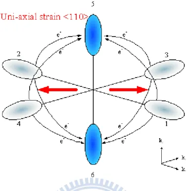
For the uni-axial strain, the sensitivity of band structure to strain is different according to the Si channel direction and orientation the transistor fabricated on. For example, devices along <100> compared to the <110> as Fig. 1-6 possesses higher sensitivity for uniaxial strain, where uniaxial strain is parallel to transport direction [1.42]-[1.43]. From the band structure, strained device along <100> as Fig. 1-7 possesses an anisotropic occupation of four fold valley. Therefore, the anisotropic occupation is responsible for the lower conductivity mass compared to <110> strained device. For the same strain coupling, the bi-axial strain induces largest band splitting and uniaxial <110> strain induces smallest one. For uniaxial strain, the curvature of conduction band near the Brillouin Zone is also relatively insensitive to strain, meaning that the carrier repopulation is the dominant mobility enhancement mechanism.
1.1.4 Hot Carrier Effects
Hot carrier, which was produced by the high lateral electric field near the drain, can generate electron-hole pairs via impact ionization. Subsequently, the hot carrier with high energy would inject into the gate oxide, and the oxide quality and interface state would be degraded [1.44]- [1.45]. Thus, the hot carrier effect would cause threshold voltage shift and degraded subthreshold swing. As the strain technique application, the altered band structure also makes influence on the hot carrier effects [1.46]- [1.48]. The higher carrier mobility in strained channels implies a lower electric field at velocity saturation. Carrier heating in the maximum field near the drain becomes easier, resulting in a higher impact ionization rate and a higher substrate current. Additionally, the band gap would be lower with strain coupling, meaning that lower energy is lost in the creation of an excess electron-hole pair.
1.1.5 Flicker Noise characteristics
The origin of the 1/f noise in MOSFET has been debated for several decades, whether mobility fluctuation noise due to the phonon scattering [1.49]- [1.50] or number fluctuation noise due to traps in the gate oxide [1.51]-[1.52]. McWorther proposed a 1/f noise model based on quantum mechanical tunneling transitions of electron the channel and traps in the gate oxide [1.53]. Since the tunneling time depends on the distance from the channel to trap, the distribution of time constants would produce 1/f noise as Eq. (1-1).
SID q2kTλNt f WLCox2
I2
( g− t)2
… … … … … … (1 − 1)
The frequency component deviates from 1 if the trap density is not uniform in depth ; 1 is observed when the trap density is higher close to the gate oxide/channel interface than that in the interior of the gate oxide and 1 for the opposite condition. The model possesses excellent agreement with experiments for NMOS than PMOS. In addition to inversion charge density fluctuation, it was later proposed that a trapped carrier also affects the surface mobility through coulomb interaction, called as correlated mobility fluctuation as Eq. (1-2). However, the correction factor as constant was criticized for being unphysically, since screening was not accounted for [1.54]- [1.55]. Instead, should be expected to decrease with increasing inversion charge density due to the screening effect.
SID q2kTλNt f WLCox2 (1 +
αμeffCoxI
g )2g2 … … … (1 − 2)
On the other hand, the mobility fluctuation theory considers flicker noise as a result of fluctuation in bulk mobility, due to phonon scattering as Eq. (1-3).
SId I2
qαHμeff
fL2I … … … … … … (1 − )
It is noted that both number fluctuation and mobility fluctuation may fail to accurately describe the LF noise data over the entire bias range. The mobility fluctuation model is often fitting in strong inversion, and the number fluctuation is more useful below and around threshold.
Recently, using SiN to improve device performance has drawn a lot of attention for a number of applications. For single crystal devices, using strain technique is a promising approach. Although using the contact etching stop layer (CESL) to couple strain into the channel is a mature technique, the SiN intrinsic-stress impact on the SMT technique and its mechanism still need clarifications. As the poly-Si pitch shrinks in high-density static random access memory circuits, the thickness of the capping layer that we can use is reduced, meaning that the mobility enhancement would be lowered with each successive generation. Therefore, choosing the appropriate material and taking advantage of the limits to the thickness of the capping layer to create the highest mobility are important issues.
On the other hand, because the grain boundaries in poly-Si TFTs have a profound influence on device characteristics and degrade carrier transport, developing promising techniques to reduce the trap density is important. Besides the involvement of strain, using a plasma deposited SiN layer as a high concentration diffusion source of atomic hydrogen is a promising approach for improving the performance of poly-Si TFTs [1.56]. These hydrogen and nitrogen radicals originating from SiN layer are effective to improve the mobility, threshold voltage, and leakage current. However, the effect of the flow rate of different reactant gases on the deposition of the SiN layer for passivation of poly-Si TFTs has yet to be systematically investigated.
Moreover, post annealing decreases the benefits of using hydrogen radicals by plasma treatment to passivate these defects, indicating that there are limits to thermal cycling after the hydrogenation process. The effects of the post annealing temperature on the poly-Si TFT performance have also been studied experimentally [1.57]. However, the effects of the hydrogen instability induced by post annealing on the passivation of tail states, the passivation of deep states, and the additional defect generation in poly-Si TFTs must be clarified.
Furthermore, the stress originating from SiN not only affects the carrier transportation, but also the crystallization. Thus, besides the hydrogen induced retardation of the crystallization, the influence of stress originating from proximity layer on device performance is very important.
1.3 Organization of the Dissertation
The organization of the thesis is separated into six chapters and organized as follows.
In chapter 1, we presented the introduction of strain techniques related to single-crystal MOSFETs and the trap reduction associated to poly-Si TFTs.
In the chapter 2, we explore a variety of SiN as the capping layer to execute SMT. Based on the material and electrical analysis, a reasonable mechanism connecting the property of SiN to the improvement of mobility would be proposed. In addition to the enhancement of performance, the impacts of SMT on the interface state, gate leakage, hot carrier stressing, and flicker noise were thoroughly studied.
In the chapter 3, this chapter presented the effect of the flow rate of different reactant gases on the deposition of the SiN layer for passivation of poly-Si. Poly-Si TFTs capped with different SiN passivation layers show differences in their performance improvements, since different mechanisms are involved. Additionally, a mechanism to explain the double hump phenomenon induced by incomplete trap passivation was proposed. Also, the immunity to positive gate bias stress, negative gate bias stress, and hot carrier stressing was reviewed in detail.
In the chapter 4, this chapter focused on the passivation efficiency of hydrogen by hydrogen-containing nitride, based on the comparison of different thicknesses of SiN or inserted TEOS oxide. Also, the impacts of hydrogen release on the threshold
voltage, mobility, and leakage were studied. Moreover, the degradation of hot carrier stressing, NBTI, and PBTI for all samples were systematically investigated. The hydrogen release make the poly-Si TFTs exhibit different characteristics of reliability, and two possible mechanisms were proposed to explain the increased pre-existing defects.
In the chapter 5, the impacts of the SiN proximity layer on the poly-Si TFT crystallized by SPC or MILC would be clarified. As a result, SPC exhibits the strong dependence on the stress, the proximity layer, and the crystallization temperature. For MILC, the SiN proximity layer not only retards the MILC growth rate, but also degrades the electrical characteristics. Three possible mechanisms can be used to explain the dependence of MILC on the proximity layer.
In the chapter 6, the results are summarized and organized. Future works will be presented based on the result of the thesis..
Fig. 1.1 2010 ITRS Process integration Devices and structures Logic potential solution
Fig. 1.2 (a) Si capped on SiGe substrate can possess biaxial strain property. (b) Contact etch stop layer induce uni-axial stain.
(a)
(b)
Si substrate oxide D S Poly-Si Tensile or Compressive SiN Relaxed Si1-xGex Si cap oxide S D Poly-Si Si substrate
Fig. 1.3 (a) SiGe S/D possessed larger lattice constant induces compressive uni-axial strain laterally into the channel (b) SiC S/D possessed smaller lattice constant induces tensile uni-axial strain laterally into the channel. (c) The poly gate thermal volume expansion induces strain memorization for SMT application.
(a)
(b)
(c)
Si substrate oxide D S Poly-Si SiN annealing Si substrate Poly-Si Si1-yCy S oxide Si1-yCy D tensile Si substrate oxide Poly-Si Si1-xGex D Si1-xGex S compressiveFig. 1.4 Silicon without strain coupling possesses six- fold degenerate valley. 5 kz kx ky 6 2 4 3 1 e -e -e- e -e- e -e -e -biaxial strain
Fig. 1.6 With <110> uni-axial strain coupling , the carrier would redistribute into ∆2 valley. 5 kz kx ky 6 2 4 3 1 e -Uni-axial strain <100> e -e- e -e- e -e -e
-Fig. 1.7 With <100> uni-axial strain coupling, the E-k relation would transfer into an anisotropic occupation of four fold valley
Chapter 2
Stress of SiN and Stress Memorization in Devices.
2.1 Introduction
Channel-strain engineering is one of the most effective remedies to boost the drive current in scaled devices [2.1].Using biaxial strain, it introduces a relaxed SiGe buffer layer using a complex process with the Ge out-diffusion issue [2.2]- [2.3].For uniaxial strain, including SiGe source/drain, [2.4]research has invented a contact etch stop layer and stress-memorization technique (SMT) [2.5]-[2.6]. Among these techniques, SMT is simpler to fabricate, compatible with conventional processes, and has the potential to combine other strain-technique advantages, owing to its memorization technique.
In recent approaches, several investigations have focused on optimization of the SMT technique by manipulating the geometrical structure and material features to obtain higher mobility. For example, SiNx offers a higher Young’s modulus than SiOx.
Hence, using SiNx as spacer or capping layer could confine an expanded poly-Si gate
firmly and sufficiently suppress lateral expansion to attain higher tensile strain coupling. The phenomenon of material expansion also plays a critical role in the SMT process. For poly-Si implantation, the deeper the Rp projection range using the same dosage, the more obvious the stress memorization [2.7], [2.8]. With a heavier implant source and the amount of dose aid, the poly-gate condition would be more amorphized [2.9]. More effective recrystallization would thus occur, and volume swelling could be enhanced significantly.
However, the SiN intrinsic-stress impact on the SMT technique and its mechanism still need clarifications. As the poly-Si pitch shrinks in high-density static random access memory circuits, the thickness of the capping layer that we can use is reduced, meaning that the mobility enhancement would be lowered with each successive generation [2.10]. Therefore, choosing the appropriate material and taking advantage of the limits to the thickness of the capping layer to create the highest mobility are important issues.
In this chapter, we explore a variety of SiN as the capping layer to execute SMT. We find that the material with the greatest potential is a compressive SiN layer rather than the tensile SiN layer that is typical of the conventional process for CESL and
SMT. Among the intrinsic characteristics of the SiN layer, the key factor is the amount of stress shift rather than the initial or final stress. The corresponding mechanism is also clarified.SMT would degrade gate leakage, but its mechanism did not clarify clearly [2.11]. To our knowledge, a few research reports the impact of initial compressive nitride on gate leakage and interface-state. This chapter also investigates interface-state passivation and the connection between gate-leakage and intrinsic stress characteristics in the SMT process. A previous work adopted Fourier-transform-infrared-spectroscopy (FTIR) for evaluating the hydrogen concentration in different kinds of nitride for SMT application. However, Ortolland presented hydrogen as an interface-state creator [2.12]. In contrast, we found that hydrogen passivation improved the interface-state. Besides performance advantage, the SMT with compressive nitride is superior for interface condition, gate-leakage concern, hot carrier stressing, and flicker noise.
2.2 Experiment
2.2.1 Material Analysis
X-ray photoelectron spectroscopy (XPS) was employed to investigate the SiNx
films as 150nm by PECVD (Plasma Enhanced chemical vapor deposition) with different deposition condition. The detail of deposition condition split was list as table 1 with RF power 100W in 137Pa. For investigating the impact of thermal annealing, all conditions execute nitrogen annealing for 30s at 900°C. The N/Si atomic ratios was obtained from the area of the N 1s peaks and that of the SiN parts of the Si 2p peaks as table 1. We found that N/Si would be higher with the higher diluent gas N2 in
the deposition process. For increasing SiH4 flux, the N/Si would increase first, and
then the ratio would decrease to Si rich SiNx as Fig. 2-1. After RTA process, SiH4 high
and N2 high would release nitrogen in the high temperature, and the N/Si atomic ratios
would decrease consequently. For the density analysis, all samples possess comparable etching rate, except Si high SiNx samples cannot be etch by phosphoric
acid. As sketched in Fig. 2-2, the chemical shifted component was analyzed by XPS. Starting with the a-Si network in which each Si is connected by four other Si atoms as nearest neighbors. As nitrogen couple into the network, an increasing number of homopolar Si-Si bonds are replaced by heteropolar Si-N bonds, meaning that the charge would transfer from Si to the more electronegative N leaves a positive charge
on the Si atom. Therefore, the Si core level would shift from 99.6eV in a-Si toward the higher binding energy, such as 102.8 as SiN1.5 [2.13]. By modulating the diluent
gas N2, composition of the peaks in the as-deposited films do not change substantially.
However, after the RTA process, the peak of lower binding energy Si 2p formed, meaning that the lower x of SiNx would form in the process with nitrogen loss.
Moreover, Fourier transform infrared spectrometer (FTIR) was adopted for investigating differences among all conditions as Fig. 2-3 and Fig. 2-4. From the area of Si-N bonding comparison, no significant difference can be detected by FTIR. After annealing, Si-N detected by FTIR would increase, and the FWHM (full width at half maximum) would get higher for all N2 modulation samples. It is noted that the
FWHM of the band reflect the overall disorder of the network topology [2.14]. Therefore, the higher FWHM reveals that the range of bond angle distortion and the absorption band would be broader. However, the FWHM of SiH4 sample would
decrease after annealing, and it is consistent with a previous report [2.14], indicating that a thermally activated reordering of the network for the nitrogen rich composition. Additionally, modulation of diluent gas makes impact on the Si-H and N-H bonding as Fig. 2-5 and Fig. 2-6. The higher the diluents gas, the lower Si-H bonding as-deposited possesses. Besides, the film deposited by lower diluent gas would break higher quantity of Si-H during annealing. However, the N-H bonding doesn’t reveal a clear dependence on the flux of diluents gas. Additionally, the SiH4 high as deposited
has the highest Si-H band among all samples and largest broken Si-H after annealing process.
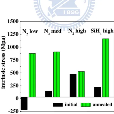
Furthermore, the characteristics of intrinsic stress are very important for device application, such as CESL and SMT process [2.15]- [2.16]. By modulating diluent gas and RF power in 137Pa, different SiNx samples deposited on 4-inch wafer were
investigated. The stress measurement was performed on a Tencor FLX-2320 system. This system evaluates the stress by measuring the change in curvature of the silicon substrate before and after process. The lower RF power performs in the deposition process, the higher tensile quantity the film possesses as demonstrated in Fig. 2-7. Besides, it is quite obvious that deposition with higher diluent gas can create higher tensile film. It is well know that the quantity of hydrogen in nitride makes influence on the intrinsic stress properties [2.17]-[2.18]. We found that nitride with lower hydrogen quantity could become more tensile in our experiment. Recently, both the intrinsic stress after annealing and intrinsic stress shift are extremely important in the
SMT fabrication process as Fig. 2-8. We observed that all samples become more tensile after RTA process. Nitride Deposited with lower RF power can achieve higher stress after RTA 900℃ for 30s;However, the film deposited by lower diluent gas with lower initial intrinsic stress achieves higher annealed stress shift as Fig. 8. In other word, the lower diluents gas N2 in the deposition process labeled as N2 low can
achieve higher stress shift potential after RTA as Fig.2-9. The H component in nitride film may play a significant role in determining the stress shift quantity, since the film with higher stress shift always possesses higher H quantity in our experiment. Finally, the impact of implantation and multi-deposition on the stress process are investigated as Fig. 2-10 and Fig. 2-11. With the RF power as 100W in 137Pa the N2 low and SiH4
high were deposited by PECVD on highly doping 4-inch wafer. Multi-deposition samples with deposition of 500Å SiN and cooling process executed three times are fabricated to compare to Once-deposition as 1500Å . For investigating implant impact, some of Once-deposition samples would also execute implantation treatment with As+(80keV with 1E15/cm2), which labeled as Implant-treatment. As a previous report [2.19], if the deposition process divides into several times, the final intrinsic stress would get higher, due to relaxation effect of the nitride. However, the Multi-deposition does not present a high intrinsic stress compared to Once-deposition in this experiment. Multiple depositions would decrease initial stress, annealed stress, and stress shift quantity for N2 low comparison;However, the stress characteristics of
SiH4 high possess slight difference. For the implantation treatment investigation, the
stress as deposited film would decrease, whether the initial stress is tensile or not. It’s consistent with the previous report, which proposed that implantation is a promising method to minimize the impact of tensile SiN on PMOS performance. Additionally, with the implantation treatment, the potential of stress shift of SiH4 could be
enhanced.
2.2.2 Device Fabrication
After RCA cleaning process, 3nm gate oxide was thermally grown on 6-in wafers in a vertical furnace. Undoped poly-Si gate (2000 Å ) was deposited, and As+(50keV with 5E15/cm2) was adopted to enable the maximum Poly Amorphorization Implantation (PAI) effect. After extension and spacer formation, four different silicon nitride (SiN) capping layers (1500 Å ) were deposited by PECVD, modulating the
flow-rate of N2 or SiH4 to confine the poly-Si gates. The power was set at 100W,
pressure was 137 Pa, and temperature was 300°C. To obtain a different intrinsic stress of SiN, the flow-rates of the N2 were set to 50, 100, and 1000 sccm with NH3 = 6
sccm and SiH4 = 50 sccm across all three. The samples were labeled N2-low, N2-med,
and N2-high, respectively. In addition, a SiH4-high sample in which the flow-rate of
SiH4 was 100 sccm, but the NH3 and N2 were 6 and 50 sccm, respectively, was
prepared for comparison. For investigating the impact of poly grain size on SMT, poly gate would deposit in different temperature effect as 550°C, 580°C, and 600°C, respectively. Later, after PAI treatment and spacer formation, the samples with silicon gate deposited by different temperature would cap by N2-med nitride. After RTA at
900°C for 30s, the source/drain and poly-Si gate were activated and the channel strain induces simultaneously. Subsequently the capping layers were removed, leaving residual strain in the channel, and standard MOSFET fabricating steps were followed to complete the final devices with channel lengths of 0.4m and 0.35m.
2.3 Results and Discussions
2.3.1 Device Performance
Figure 2-12 illustrates the value of transconductance divided by capacitance, to make the strain contribution to mobility clearer. We found that the N2-low split shows
the highest enhancement, 27%, while the N2-high split exhibits the lowest
enhancement, 10%. In addition, the SiH4-high sample also shows a 23% improvement.
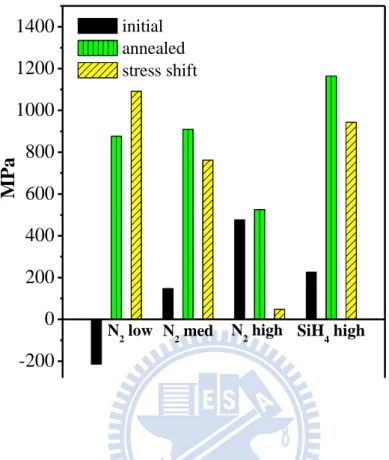
Figure 2-13 demonstrates the stress characteristics of all capping layers on 6-inch wafer for comparison as initial-stress, final-stress, and stress shifts (defined as final-stress – initial-stress). The different SiN splits have a comparable etching rate in hot H3PO4 solution, and thus the films have analogous density.
This investigation was focused on a compressive SiN layer rather than TEOS oxide or tensile SiN layer was used to execute SMT. After the annealing process, all SiN splits became more tensile. As shown in Figure 2-12, the compressive SiN, N2-low, that we used offered the greatest enhancement of mobility, instead of the
highest tensile capping layer as is conventionally used. This result is contradictory to the usual practice of optimizing the tensile capping layer to enhance NMOS mobility. Based on the experimental results, we postulate a model to clarify the mechanism.
Previous research shows that we should use a material with a higher Young's Modulus as a spacer to confine the expanded poly gate, and use the PAI technique to make the grain recrystallize effectively. In this experiment, we thoroughly investigate the capping layer and postulate another mechanism for enhancing mobility. N2-high and
N2-low possesses Young’s modulus as 166.562Gpa and 149.386Gpa, respectively. In
conventional SMT as shown in Figure 2-14, the poly-Si gate in the RTA process expands its volume by an abrupt increase in temperature, and tends to be more compressive due to confinement of volume by the spacer and capping layer wrapping. Subsequently, the poly Si gate expands its volume into the channel region during annealing process. The channel eventually becomes vertically compressive and subsequently tends to be tensile. However, N2-high doesn’t show a higher mobility
than that of N2- low one, which is not consistent when Young’s modulus considered
solely. Our experiment results show that the capping layer also plays an obvious role, in addition to the poly-Si thermal expansion condition. Since N2-low and SiH4-high
splits possessing higher stress shift have higher mobility, the benefit of mobility enhancement is the split with the highest stress shift instead of the original or final, most tensile, capping layer. It is found that the film with the highest stress shift tends to compress the channel more during the annealing process as shown in Figure 2-15. This is consistent to the model that the larger the shift of stress, the higher the vertical stress shift [2-5]. The highest stress shift in vertically results in the largest compressive strain gain vertically, making the channel become more tensile horizontally, and enhancing the electron mobility in return. Consequently, not only the volume confinement during annealing as traditional viewpoint, but also the intrinsic stress shift of capping layer make influence on the SMT technique.
The mechanisms we explore, along with the results we have obtained, indicate the existence of a greater variety of choice for the optimization of SMT. Since the compressive SiN layer we use possesses the greatest stress shift potential, the choice of materials for optimization is now broader. Figure 2-16 shows the IDS-VGS
characteristics. All devices display a similar subthreshold swing in the Vg=0.05V
condition, which implies an identical interface at the oxide/substrate for capping layer optimization.
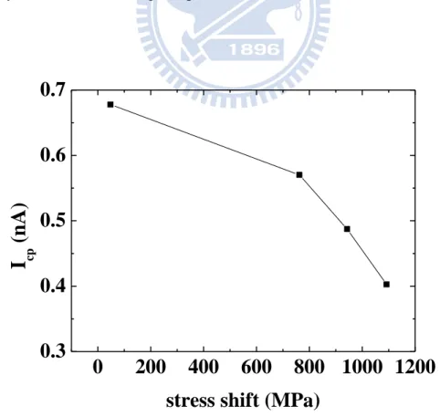
Figure 2-17 shows the measured charge-pumping current of different samples. All samples made using the SMT process show a more reduced interface-state than the control sample. To investigate the interface-state passivation as shown in Figure
2-17, we measured initial and annealed samples using FTIR (Figure 2-5and 2-6). The initial FTIR spectrum (Fig. 2-5) shows that the SiH4-high sample exhibits a high Si–H bond, while the N2-low, -med, and -high samples show a high N–H bond. The higher the N2 flow-rate during deposition, the lower the amount of H coupled into the capping layer. The initial quantity of hydrogen in the deposited capping layer plays an important role for passivating the interface-state;[2-20]-[2-21] However, Ortolland proposed that hydrogen is an interface-state creator for SMT investigation [2-12]. Stathis investigated the impact of hydrogen diffusion on different oxide condition and proposed that hydrogen would either induce interface-state or passivate the interface-state, depending on the initial interface property. At oxide interface, there is a single variety of silicon dangling bond defect, the Pb center. Pb centers are generated by Ho in a sample with initial low Pb density and reduced (passivated) if the initial Pb density is high [2-22].We investigated the impact of hydrogen on silicon dioxide rather than the impact of hydrogen on oxynitride and high-k materials as Ortolland’s work [2-12]. As a result, the impact of hydrogen diffusion in SMT on interface-state condition depends on the initial oxide condition. Figure 2-6, which shows decreased concentrations of Si–H and N–H compared to initial composition, reveals that the annealing process had significant impact on the H-component. Higher N2 flow also affects the quantity of hydrogen release during annealing. We believe
that the Si–H and N–H break release hydrogen into the channel during the annealing process. The released hydrogen passivates the dangling bonds in the annealing process, in addition to passivation by hydrogen coupling during the deposition process. For the standard SMT process, the device with a capping layer undergoes high temperature annealing during strain memorization, and the released hydrogen of this capping layer further passivates the interface-state. Consequently, the amount of passivated dangling bonds depends not only on the initial capping layer component but also on the amount of hydrogen released during the annealing process.
Besides, we found that the intrinsic stress shift of nitride also has strong dependence on the ability of passivating dangling bonds as Fig. 2-18. The film with higher hydrogen released, which always possesses higher intrinsic stress shift, could further passivate the interface states. Thus, the passivation ability is partly responsible for clarifying the connection between the intrinsic stress shift and mobility gain.
Beside the mechanism of different capping layer, the composition of poly gate also play a key role for determining the strain coupling based on different