國 立 交 通 大 學
電子工程學系電子研究所
碩 士 論 文
應用於 Serial ATA 之全數位展頻時脈產生器
及數位可程式化之高斯時脈產生器
All Digital Spread Spectrum Clock Generator
for Serial ATA Application
& Digital Programmable Gaussian Clock Generator
研 究 生:莊 立
指導教授:周 世 傑
應用於 Serial ATA 之全數位展頻時脈產生器
及數位可程式化之高斯時脈產生器
All Digital Spread Spectrum Clock Generator
for Serial ATA Application
& Digital Programmable Gaussian Clock Generator
研 究 生:莊 立 Student:Li Chuang
指導教授:周世傑 Advisor:Prof. Shyh-Jye Jou
國 立 交 通 大 學
電子工程學系 電子研究所碩士班
碩 士 論 文
A Thesis
Submitted to Department of Electronics Engineering & Institute of Electronics
College of Electrical and Computer Engineering National Chiao Tung University
in Partial Fulfillment of the Requirements for the Degree of
Master of Science In
Electronics Engineering March 2010
Hsinchu, Taiwan, Republic of China
應用於
Serial ATA
之全數位展頻時脈產生器
及數位可程式化之高斯時脈產生器
研 究 生 : 莊 立 指 導 教 授 : 周 世 傑 博 士
國立交通大學
電子工程學系 電子研究所碩士班
摘要
在這篇論文中,我們聚焦於利用輸入調變方式的全數位時脈展頻電路.為了產 生較快頻率以及較小頻率展頻量的調變時脈,我們提出了一個新的 Domino 調變 方式.我們產生出來的調變時脈.可以提升至 100MHz 以及 5000ppm 的展頻量.相比 之下,之前發表的論文其調變時脈只有 23MHz 以及 3%.在架構設計上,我們也提 出一個新的粗細混何的數位延遲線.此架構相可以節省 330%以及 383%的功率消 耗及面積.我們提出的數位展頻時脈產生器(AD-SSCG)有成為矽智財(IP)的潛力. 因為其電路都是由數位電路所設計的.這個 AD-SSCG 矽智財被用來與一 個 1.2GHz 以及一個 3GHz 的 PLL 在做模擬,都可以成功產生展頻.最後我們把 AD-SSCG 與一個 3GHz 的 PLL 利用 UMC 90 奈米 1P9M 的製程實現.AD-SSCG 所佔的 面積是 335um × 105um 其功率消耗是 2.9mW.利用 hspice post-sim 模擬 3GHz 的 EMI 下降量為 22dB.最後,我們提出的一個數位高斯時脈產生電路,它是設計給 CDR 作測試使用. 高斯時脈生器使用了高斯雜訊產生器,並把這個雜訊轉換成一個高斯時脈.產生
的高斯時脈有著調整它 jitter 大小的能力,以用來驗證 CDR 在不同環境的需要. 我們將提出的高斯時脈產生器合成於 FPGA 發展板.我們可以將資料驗証量提升 到 1012
All Digital Spread Spectrum Clock Generator
for Serial ATA Application
& Digital Programmable Gaussian Clock Generator
Student:Li Chuang Advisor:Prof. Shyh-Jye Jou
Department of Electronics Engineering
Institute of Electronics
National Chiao Tung University
ABSTRACT
In the thesis, we focus on the AD-SSCG (All Digital Spread Spectrum Clock Generator) modulation method with input reference. In order to achieve higher frequency and less frequency deviation, we propose a new Domino modulation method. We can improve the modulated clock to 100MHz and 5000ppm of frequency deviation as compared to 23MHz modulated clock and 3% of frequency deviation is published before. In the architecture design, we propose a novel Coarse-Fine DDLi (Digital Delay Line) structure, it improve the power and area by 330% and 383% than traditional structure. The AD-SSCG has the potential to become an IP because all of the circuits are deigned by digital circuit. This IP is used to work with a 1.2GHz and a 3GHz PLL, and both of them can spread spectrum successfully. Finally, our AD-SSCG and a 3GHz PLL are implemented with UMC-90-CMOS 1P9M process.
The area and power of AD-SSCG are respectively 335um × 105um and 2.9mW, and the EMI reduction of 3GHz PLL is 22dB by hspice post-sim simulation.
Finally, a proposed digital programmable Gaussian clock generator is designed for CDR (Clock and Data Recovery Circuit) testing. The Gaussian clock generator uses Gaussian noise generator to transforms a clock to a Gaussian clock. The generated Gaussian clock has the ability of controlled jitter to verify CDR with different environments. By using the proposed Gaussian clock generator on a FPGA board, we can easily verify the performance of the CDR to 1012 data to check the Bit ERROR Rate (BER).
致謝
謝謝這幾年周世傑老師對我的指導以及照顧,老師是一個對自己要求嚴格的, 總是讓我可以學到許多態度,希望老師未來可以激發出更多交大人的潛能,並且 能夠健康快樂的工作、生活。除此之外,也非常感謝李鎮宜教授、蘇朝琴教授以 及黃錫瑜教授能夠來參加我的畢業口試,給予我論文更多的幫助以及指導。 要感謝的人非常的多,首先感謝的是 TOTORO 學長,學長對我在作研究上很大 方的幫助,除此之外也很感謝明賢學長、誠文學長、庭楨學長、紹維學長、spice 學長、阿樸學長,也很感謝跟我同屆的同學舒榮、ABC、祥甡、運祥,也很開心 因為認識范姜、阿九以及奕瑋,使我在實驗室又有更多的樂趣。最後也很感謝其 他實驗室的朋友勖哲、篤雄、致煌、至中、魏胖、阿光,有了大家研究所的生活 可是又開心又充實。 當然我要謝謝父母奶奶弟弟,家人對我的支持,在這一路上不斷的栽培及鼓勵 我,使我一路可以專心讀書,也才有機會考上交通大學,更有機會得到這個交大 碩士的學位,之後出社會,會把從交大這邊學到的態度,繼續往前走。 莊立 新竹交大 2010.3.10Contents
Chapter 1 Introduction ...
1
1.1 Backround ... 1
1.2 Motivations and Goals ... 2
1.3
Thesis Orgination
...
3Chapter 2 Basic Concept of Spread Specteum Clock Generator ... 4
2.1 The Backround of EMI Problem ... 4
2.2 Concept of Spread Spectrum Clock ... 5
2.3 Sread Sprectum Parameters ... 6
2.3.1 Spread Spectrum Modes and Amounts ... 6
2.3.2 Modulation Profile ... 7
2.3.3 Modulation Frequency ... 8
2.3.4 Timing Impacts ... 9
2.4
Different Types of Spread Spectrum Clock Generator
...
11Chapter3 Proposed All Digital Spread Spectrum Clock Generator ... 16
3.1 Introducation ... 16
3.2 The Concept of Domino AD-SSCG ... 17
3.3 The Design of Domino AD-SSCG ... 22
3.3.1 The Design of Modulated Clock ... 22
3.3.2 The Solution to Overcome Infinite Digital Delay Line ... 25
3.3.3 The Dummy Delay Line Structure ... 28
3.4 The Formula for Domino AD-SSCG ... 29
3.5 Specifications of Domino AD-SSCG... 31
3.6 The Behavior Simulations of AD-SSCG +1.2GHz PLL
...
323.6.2 Down Spread Mode ……….35
3.6.3 Up Spread Mode ….……….39
3.7 The Parameters Optimaztion of Domino AD-SSCG
...
423.8 The Performance Comparision
...
48Chapter 4 The Circuit Implemenatation of AD-SSCG ... 54
4.1 The Pseudo SSCG Square Wave ... 54
4.2 The Algorithm of AD-SSCG ... 56
4.3
Proposed Novel Coarse-Fine Delay Line Struture
...
584.4 The PVT Immunity Design Method ... 61
4.5 Architecture and of AD-SSCG ... 64
4.5.1 Control Implementation ... 65
4.5.2 DDLi and dummy DDLi implementation ... 67
4.6 The Glitch Issue ... 70
4.7 Experimental Results ... 73
4.7.1 Circuit Simulation ... 73
4.7.2 Layout ... 82
4.7.3 Measurement Enviroment Setup ... 83
4.8 Comparison an Conslusion ... 84
Chapter 5 All Digital Programmable Gaussian Clock Genertor ... 88
5.1 Introduction ... 88
5.2 The Concept of Digital Programmable Gaussian Clock Generator ... 89
5.3 Gaussian Noise Generator... 92
5.3.1 Gaussian Algorithm of Box-Muller ... 92
5.3.2 The Modified Box-Muller Algorithm for CDR Application ... 95
5.3.3 Hardware Implemntation of Gaussian Noise Generator ... 96
5.5 Circuit Implementation of Programmable Gaussian Clock Generator ... 101 5.6
Experimental Measurement
... 105
List of Figures
Fig. 2.1 FFC EMI peak limit [1] ………4
Fig. 2.2 Spectrum of (a) un-spread spectrum signals (b) spread spectrum signals…..5
Fig. 2.3 (a) Central-spread (b) Up-spread (c) Down-spread……….6
Fig. 2.4 Spectrum of (a) Sinusoidal profile (b) Triangular profile……….8
Fig. 2.5 Spread spectrum with different modulation frequency……….9
Fig. 2.6 Time domain behavior………9
(a)Un-spread spectrum signals (b) Spread spectrum signals Fig. 2.7 Cycle-to-cycle jitter………10
Fig. 2.8 Long-term jitter………11
Fig. 2.9 SSCG of modulation on VCO………..12
Fig. 2.10 SSCG of modulation on divider………...12
Fig. 2.11 SSCG of phase selection………..13
Fig. 2.12 SSCG of modulation on input reference………14
Fig. 3.1 The modulation method of paper [12]………..17
Fig. 3.2 The proposed Domino AD-SSCG………...18
Fig. 3.3 Digital Delay Line (DDLi)……….22
Fig. 3.4 Modulated clock with wider period………23
Fig. 3.5 Modulated clock with narrower period………..24
Fig. 3.6 The DDLi with delay time which is little more than one period…………...25
Fig. 3.7 (a) “next Clock” and “present clock” on DDLi………..27
(b) “present Clock” and “previous Clock” on DDLi Fig. 3.8 DDLi and rising edge detecting circuit ………..27
Fig. 3.10 DDLi and dummy DDLi with uniform delay cell……….29 Fig. 3.11 (a) Simulink model of AD-SSCG+PLL……….32 (b) Simulink model of AD-SSCG
Fig. 3.12 Two pulse signals to complete a modulated clock………..33 Fig. 3.13 The time diagram of modulated_CLK when “Carry=0 and 1”…………..34 Fig. 3.14 Frequency of 1.2GHz VCO………35 Fig. 3.15 (a) Frequency of VCO with 5000ppm and down mode……….36 (b) Spectrum of VCO with 5000ppm and down mode
Fig. 3.16 (a) Frequency of VCO with 10000ppm and down mode………37 (b) Spectrum of VCO with 10000ppm and down mode
Fig. 3.17 (a) Frequency of VCO with 15000ppm and down mode………38 (b) Spectrum of VCO with 15000ppm and down mode
Fig. 3.18 (a) Frequency of VCO with 5000ppm and up mode……….39 (b) Spectrum of VCO with 5000ppm and up mode
Fig. 3.19 (a) Frequency of VCO with 10000ppm and up mode………..40 (b) Spectrum of VCO with 10000ppm and up mode
Fig. 3.20 (a) Frequency of VCO with 15000ppm and up mode………41 (b) Spectrum of VCO with 15000ppm and up mode
Fig. 3.21 The modulation scheme of different N and M………..43 (a)N=2 M=8 (b) N=4 M=4 (c) N=8 M=2
Fig. 3.22 Re-combination of modulation_CLK when N=2 M=8………43 Fig. 3.23 The modulation scheme of assuming N×M =64……….44
(a) N=8 M=8 (b) N=16 M=4 (c)N=32 M=2
Fig. 3.24 Frequency of VCO with down spread mode and 10000ppm frequency deviation (a) N=M=40 (b) N=80 M=20 (c) N=160 M=10 ………45
Fig. 3.25 Spectrum of VCO with down spread mode and 10000ppm frequency
deviation (a) N=M=40 (b) N=80 M=20 (c) N=160 M=10………...47
Fig. 3.26 Simulink model of AD-SSCG of paper [12]………49
Fig. 3.27 Frequency of VCO with down spread mode and 10000ppm frequency deviation (a) paper [12] with 40 steps (b) proposed method with 40 steps (c) paper [12] with 10 steps ………...50
Fig. 3.28 Spectrum of VCO with down spread mode and 10000ppm frequency deviation (a) paper [12] with 40 steps (b) proposed method with 40 steps (c) paper [12] with 10 steps………52
Fig. 4.1 Conventional PFD circuit……….55
Fig. 4.2 Comparison of modulated clock and pseudo modulated clock………55
Fig. 4.3 Comparison of modulated_CLK and pseudo modulated_CLK………55
Fig. 4.4 The algorithm of AD-SSCG……….57
Fig. 4.5 (a) Uniform DDLi structure………..59
(b) Coarse-Fine DDLi structure Fig. 4.6 (a) Clock rising edge on DDLi with PVT variation in down mode………...61
(b) Clock rising edge on DDLi with +/- 15% PVT Variation in down mode Fig. 4.7 DDLi and dummy DDLi in down mode………..62
Fig. 4.8 (a) The clock rising edge on DDLi with PVT variation in up mode……….62
(b) The clock rising edge on DDLi with +/- 15% PVT variation in up mode Fig. 4.9 DDLi and dummy DDLi in up mode………63
Fig. 4.10 Overall architecture of DDLi and dummy DDLi………63
Fig. 4.11 The overall architecture of AD-SSCG………65
Fig. 4.12 The circuit of control………66
Fig. 4.14 Simulation of control circuit of case2 (pre-sim)………67
Fig. 4.15 The circuit of DDLi and dummy DDLi……….68
Fig. 4.16 (a) The circuit of C_BUF (b) The circuit of TRI_INV………68
Fig. 4.17 The delay dime of F_BUF (post_sim)……….69
Fig. 4.18 (a) The delay waveform of C_BUF (post_sim)………69
(b) The delay time of C_BUF (post_sim) Fig. 4.19 (a) Phase switching from “leading phase” to “lagging phase”………70
(b) Phase switching from “lagging phase” to “leading phase” Fig. 4.20 The delay path to from “Position Decision” to “Decoders”……….71
Fig. 4.21 The unstable value output of “Position Decision”………72
Fig. 4.22 The solution for glitch of unstable output value………...72
Fig. 4.23 The architecture of revised AD-SSCG……….73
Fig. 4.24 Frequency of 3GHz VCO……….74
Fig. 4.25 (a) Frequency of 3GHz VCO with 5000ppm and down mode……….75
(b) Spectrum of 3GHzVCO with 5000ppm and down mode Fig. 4.26 Vc lock-in simulation of 3GHz PLL (post-sim)………77
Fig. 4.27 The full-swing output of 3GHz PLL (post-sim)………77
Fig. 4.28 The output of 3GHz BUF (post-sim)……….78
Fig. 4.29 Peak-to- peak jitter of 3GHz PLL (post-sim)……….78
Fig. 4.30 Vc of 3GHz PLL with triangular profile (post-sim)………...79
Fig. 4.31 Peak-to-peak jitter of 3GHz PLL with spread spectrum (post-sim)………79
Fig. 4.32 The spectrum of 3GHz PLL with and without spread spectrum (post-sim).80 Fig. 4.33 Spectrum of 100MHz AD-SSCG square waveform and 100MHz square waveform (post-sim)………80
Fig. 4.35 Layout of AD-SSCG……….82
Fig. 4.36 Test environment setup……….83
Fig. 5.1 (a) higher frequency clock (b) normal divided clock with 50% duty cycle,..90
(c) divided clock with assigned number is #63 (d) divided clock with assigned number is a Gaussian random variable. Fig. 5.2 The brief architecture of programmable Gaussian clock generator…………91
Fig. 5.3 150000 samples with non-uniform LUT Box-Muller algorithm …...………94
(a)w.o. and(b) w.i. Central Limit Theorem. Fig. 5.4 Overall architecture of Gaussian Noise Generator……….97
Fig. 5.5 The relative position of clock rising edge with different value……….97
Fig. 5.6 (a) N-2N Decoder (b) The “Decoder Pulse” of N-2N Decoder………99
Fig. 5.7 The connection between N-2N Decoder to 2N shift-register………99
Fig. 5.8 An example of pulse signal with different input of Decoder Input ………...99
Fig. 5.9 (a) Pulse signal and clock signal………100
(b) Pulse to clock recovery circuit (c) The time diagram of pulse to clock recovery circuit Fig. 5.10Overall architecture of Gaussian clock generator circuit………102
Fig. 5.11 Gaussian CLK example with different division ratio……….102
(a) higher frequency CLK (b)Gaussian clock with division 8 (c) Gaussian clock with division ratio 16 Fig. 5.12 Gaussian Clock Generator with embedded verification circuit………….104
Fig. 5.13 Gaussian CLK (a)
σ
c = 0.04UI (b)σ
c = 0.02UI (c)σ
c = 0.01UI……104Fig. 5.14 Test environment setup……….106
List of Tables
Table 2.1 SATA-2 specifications [1]………..…………5
Table 3.1 BUF delay in different clock frequency and frequency deviation…………19
Table 3.3-1 The specification of 1.2GHz PLL [13]………34
Table 3.3-2 The simulation result of 1.2GHz PLL [13]………35
Table 4.1 The parameters of 3GHz PLL [15]………74
Table 4.2Design summary of proposed AD-SSCG+3GHz PLL………..81
Table 4.3 Design summary of proposed AD-SSCG……….81
Table 4.4 Comparison of SSCG with different modulation method………85
Table 4.5 Comparison of SSCG with input reference modulation………87
Table 5.1 Parameters of Gaussian random variable N………..96
Table 5.2 Different hardware structures with different division………96
Table 5.3 Different hardware structures with different division ratio………103
Table 5.4Different standard deviation Gaussian CLK with relative coefficient……103
Chapter 1
Introduction
1.1 Background
Technology scaling has dramatically increased the amount of computation. The
increased computation of digital circuit in SOC will require higher bandwidth to
transmit signal. As a result, the design of chip I/O has became increasingly
sophisticated, with multi-Gb/s bandwidth to provide higher computation mount of
systems and networks. The higher speed serial link is composed of (1) transmitter, (2)
channel, and (3) receiver. The transmitter use high speed PLL with multi-phase to
transmit high bandwidth signal. When the signal passes through the channel which
often has poor frequency response at high frequency, the signal will decrease at the
part of high frequency. In the receiver end, we could use equalizer to compensate the
loss due to the channel. The equalized signal will pass through CDR (clock data
recovery circuit) to recover correct data which is the original bitstream from
transmitter end. The consideration of system design includes the noise of transmitter
signal, channel design, package design, signaling method, equalization, and CDR
specification. Another important issue shall be highlighted. When PLL generates
higher frequency clock, it often brings more EMI (electron magnetic interference)
problem. The solution to implement of high speed PLL, we can spread this high speed
bandwidth to reduce EMI problem. The specification of SATA [1] also sets the
limitation that the EMI reduction needs to be larger than 7dB. However, the new
challenge will be generated both in transmitter and receiver at the same time because
the CDR must recover the data with intrinsic deterministic jitter due to that the
transmitter use spread clock to transmit the signal.
1.2 Motivations and Goals
There is a publication [12] of SSCG with input reference modulation on JSSC 2007.
The paper names “All Digital Spread Spectrum Clock Generator” because all of the
circuits are designed by digital circuits. This modulation method has significant
difference among SSCG modulation methods. All of the other modulations do the
modulation profile in PLL loop with analog approach. But paper [12] only uses digital
approach outside of the PLL loop to generate spread spectrum clock. After reading
this paper [12], we think this kind of modulation method can be implemented as an IP
(Intellectual Property). Thus, firstly we want to implement our AD-SSCG (all digital
spread spectrum clock generator) which can have different spread modes, like up and
down, and have different frequency deviation for different required specifications.
Secondly, we think the frequency of the generated modulated_CLK of paper [12] is
too slow, our goal is to increase the frequency of the modulated_CLK. Thirdly, for
SATA applicat ion, the frequenc y deviat ion is less than paper [12], so we
need to present a solution to achieve less freque ncy deviation.
Besides the research of AD-SSCG, we also interest in the topics o f CDR testing.
Often, the BER (Bit Error Rate) will be estimated by two methods (1) after chip
tape-out, we use equipment BERT to generate high speed clock with Gaussian noise
the BER of CDR. The method (2) will verify the system robustly but the verification
platform is implemented on computer. It is limited by hardware capacity and limited
memory so the testing data amount only can achieve around 106. In order to solve the
problem of testing in pre-tape out procedure, we use Gaussian noise generator and
some digita l circuits to construct a Gaussian noise clock generator with the
controllability of different jitter. All of these circuits are designed by digital circuits so
it can be implemented on FPGA developed board. We use this new testing platform to
breakthrough the amount of testing data.
1.3 Thesis Organization
Chapter 2 will introduce the basic concept of SSCG and four main kinds of
modulation methods. Chapter 3 will analyze the SSCG with input reference method
and make comparisons between paper [12] and ours. We will construct simulink
model to compare the performance. Chapter 4 will introduce the implementation
method of our AD-SSCG and design consideration. Then, the experimental results
and SSCG performance comparisons are also in this chapter. Chapter 5 will show the
Chapter 2
Basic Concept of Spread Spectrum Clock
2.1 The Background of EMI Problem
Today, electrical devices have more Electromagnet ic Inter ference (EMI) at
operational frequency. EMI will pollute radio spectrum which is caused by the
radiation of unwanted radio frequency signals. EMI will occur in those electronic
systems that change voltages and current rapidly. Thus, the Federal Communications
Commission (FSS) in the United States has regulation rules about the maximum
power of EMI [1] as shown in Fig. 2.1. The regulation rules focus on the peak power,
not on the average power.
Fig. 2.1 FFC EMI peak limit [1]
The required high speed clock will have high frequency component. The metal line in
chip will suffer from the EMI phenomenon. In the field of serial link, the specification
of SATA-2 [2] also defines the EMI requirement. Table 2.1 shows the SATA-2
specification. The EMI has to be reduced by 7dB at least. Then, the SATA-2
specification also defines the spreading mode, amount and modulation frequency.
Table 2.1 SATA-2 specifications [2]
Parameter Value
EMI reduction >7 dB Spread spectrum mode Down Mode
Spread amount 5000 ppm Modulation frequency 30 ~ 33 KHz
2.2 Concept of Spread Spectrum Clock
The basic idea of the spread spectrum clock is to slightly modulate the frequency of
clock signals and the energy of the signals will be scattered to a controllable wide
range. The energy is distributed by modulating the signal slowly between two
frequency boundaries. The peak energy of every harmonic component in the spectrum
is decreasing after spreading spectrum. Fig.2.2 shows the signal with and without
spread spectrum [3].
2.3 Spread Spectrum Parameters
2.3.1 Spread Spectrum Modes and Amounts
There are three main kinds of spread spectrum modes, center-spread, down-spread,
and up-spread.
We define the parameter firstly. The parameter fn is the central frequency. The parameter δ is the total amount of spreading as a relative percentage of fn. For central-spread modulation, the frequency starts at fn, and the frequency varies from f (1n 1δ)
2
to f (1n 1δ) 2
as shown in Fig. 2.3 (a). For the up- spread modulation, the frequency varies from fn to
f (1 δ)
n
as shown in Fig. 2.3 (b). For the down-spread modulation, the frequency varies from fn to f (1 δ)n as shown in Fig. 2.3 (c). In Fig. 2.3, we will find parameterf
mwhich is defined as modulationFig. 2.3 (a) Central-spread (b) Up-spread (c) Down-spread
For SATA- 2 exa mp le, δ =5000ppm wit h down- spread mod ulat ion, a nd
m
f
=30~33KHz. Thus, if we usef
n with 1.2GHz, the frequency of modulated clock varies from 1.2GHz to 1.194GHz. The modulation period is the inverse of 30KHz to33KHz, that is, 33.33us to 30.30us.
2.3.2 Modulation Profile
The modulation profile is one of the important parameters that affect the
performance of spread spectrum. The shape of mod ulation profile determines the
distribution of energy. In other words, the modulation profile in time domain
determines the shape of power energy in frequency domain.
Fig. 2.4 shows two common modulation profiles. For the sinusoidal modulation,
we can find out that the peak in two sides of spectrum is larger than central spectrum.
For the triangular modulation, the peak in two sides is larger than central spectrum,
but the difference of spectrum height between two sides and central point is less than
that of sinusoidal modulation. We can observe that in the sinusoidal modulation, the
location time of more maximum and minimum frequency is longer than triangular
modulation. In EMI standard, we care about the peak of spectrum, not average power.
Fig. 2.4 Spectrum of (a) Sinusoidal profile (b) Triangular profile
2.3.3 Modulation Frequency
The modulation frequency is an important factor that will affect the EMI reduction
performance. In the main stream, the modulation frequency is between 30 to 50KHz.
The higher modulation frequency will have better EMI reduction performance as
shown in Fig. 2.5 for Matlab simulation. Although the higher modulation frequency
will have more EMI reduction, the modulation frequency is limited due to the timing
jitter of the clock source and the tracking capability of the timing recovery in the
Fig. 2.5 Spread spectrum with different modulation frequency
2.3.4 Timing Impacts
In a SSCG system, the frequency varies with time as shown in Fig. 2.6 (b). For
serial link application, we will use spread spectrum clock in transmitter and receiver.
We must know the tolerance of the system for changing of clock. So, we need to
know some important parameters, like cycle-to-cycle jitter and long term jitter [3].
Fig. 2.6 Time domain behavior
(a)Un-spread spectrum signals (b)Spread spectrum signals
A. Cycle-to-Cycle Jitter
When we use spread spectrum clock, the frequency will vary with time. The
period of every clock will increase or decrease continuously. So, every clock has
different period. The definition of cycle-to-cycle jitter is the difference between
Fig. 2.7 Cycle-to-cycle jitter
We will use a formula to calculate cycle-to-cycle jitter [4] for down spread mode
which is the case for SATA-2 specification. Firstly, we calculate the period difference
between normal frequency and maximum modulation frequency in Equation (2.1).
total n n n 1 1 δ = -(1-δ)f f f ΔT (2.1) Then, we calculate the number of clocks in half time modulation. The frequency
changes from
f
n tof (1-δ)
n in half t ime modulat ion. Equat ion (2.2) will calculate the number of clocks in half time of the modulation cycle.avg m avg m f 1 1 2f f 2f N= (2.2) where
f
m andf
avg are the modulation and average frequency of the spread spectrum clock. We adopt the triangular modulation profile to calculate the averagefrequency as shown in Equation (2.3).
n
avg=(1-0.5 ) f
f
δ
(2.3) Therefore, the cycle-to-cycle jitter can be expressed as shown in Equation (2.4).total m c-c n n m 2 n ΔT δ 2f ΔT = = × N f (1-0.5δ)f 2f δ = (1-0.5δ)f (2.4)
For a 1.2GHz spread spectrum clock with 5000ppm frequency deviation and
31KHz modulation frequency, the cycle-to-cycle jitter is shown in Equation (2.5).
3 16 c-c 9 2 2 31 10 0.5% ΔT 2.15 10 (1 0.5 0.5%)(1.2 10 ) = 0.215 fs (2.5)
B. Long-Term Jitter
Long-term jitter defines the maximum cycle change form its ideal position as
shown in Fig. 2.8. Equation (2.6) shows the long-term jitter of clock 1.2GHz with
5000ppm frequency deviation [4].
Fig. 2.8 Long-term jitter
12 total 9 nom δ 0.5% ΔT 4.166 10 f 1.2 10 4.2 ps (2.6)
2.4 Different Types of Spread Spectrum Clock Generator
A basic PLL is comprised of PFD, CP, LPF, VCO and Divider. Due to EMIproblem, PLL need to have spread spectrum function. There are four common
modulation methods [4]: (1) modulation on VCO, (2) modulation on Divider, (3)
phase selection of multiphase VCO, and (4) input reference modulation.
Fig. 2.9 shows the SSCG of modulation on VCO. In this method, we often need
another CP to generate voltage of triangular voltage on Vctrl as modulation profile.
Because we know the relation between the Vctrl and frequency of VCO, we could
know the required voltage profile to add. The paper [5-7] adopt this modulation
method. However, this modulation method will be serious distorted with process
variation. For example, the Kvco curve and the current amount of CP will be changed
Fig. 2.9 SSCG of modulation on VCO
Fig. 2.10 shows the SSCG of modulation on Divider. The mechanism is that the
Divider changes the divider ratio, and the frequency of VCO will change from
original frequency to spreading spectrum frequency. Often, there are many steps
between original divider ratio (N) and spreading spread divider ratio (N+n). More
steps of division ratio will make the triangular profile like an ideal one and have better
EMI reduction. Paper [8] and [9] use fractional delta-sigma multi- modulus divider
and FDMP (Frequency Dual-Modulus Prescaler) to increase the steps. The feature of
this method needs to have a Divider with large division modulus. The divider ratio has
an impact on the loop characteristic of the PLL. Thus, it is difficult to have N that is
shooting for both the specification of PLL and SSCG.
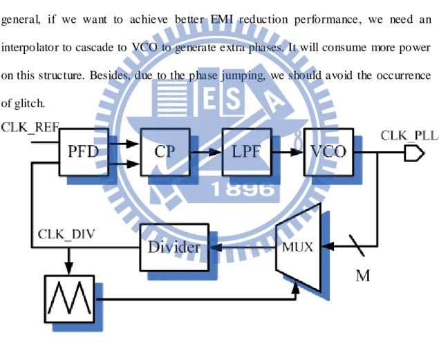
Fig. 2.11 shows the SSCG of phase selection of multi-phase VCO. It needs a
MUX to connect the multi-phase clock of VCO. We can design the numbers of cycles
to jump one phase to determine frequency spread spectrum amount. The mechanism
is that when MUX jump to the next phase, it will let the Divider be triggered fast.
When PFD will find the feedback CLK_DIV is faster than CLK_REF, PFD will show
DW signal to reduce the frequency of VCO. The gradual jumping phase will make
PLL have spread frequency function. Paper [10] and [11] adop t this modulation
method. The structure of this modulation method needs a multi-phase VCO. In
general, if we want to achieve better EMI reduction performance, we need an
interpolator to cascade to VCO to generate extra phases. It will consume more power
on this structure. Besides, due to the phase jumping, we should avoid the occurrence
of glitch.
Fig. 2.11 SSCG of phase selection
Fig. 2.12 shows the SSCG with input reference modulation. Firstly, the reference
clock signal (CLK_REF) passes through a SSCG block and SSCG generates
modulated_CLK. A PLL is used to track this modulated_CLK and will have spread
dec ided by t he SSCG. Paper [12] s hows t hat the PLL tracks a 23M Hz
modulated_CLK and finally the 148.5MHz VCO has 13dB EMI reduction with 3%
frequency deviation. In this SSCG modulation method, PLL designer can focus on the
design of PLL, and don‟t need extra effort to consider spread spectrum function. The
only concern of the PLL is to have the ability to track the modulated_CLK. Moreover,
due to the operation of SSCG is on Freq_REF which is much smaller than Freq_PLL, this
SSCG can be designed by all digital circuit approach (AD-SSCG).
Fig. 2.12 SSCG of modulation on input reference
The thesis will focus on the method of modulation on input reference and design
this SSCG by all digital circuits (AD-SSCG). Besides, we will improve the
performance compared to paper [12], for example, we could generate higher
frequency modulated_CLK with less frequency deviation. The AD-SSCG will
become an essential IP for PLL. Firstly, the AD-SSCG is implemented by digital
circuit shall have programmable capability. For example, we can design different
(1)frequency deviation, (2)modulation frequency, (3)frequency of modulated_CLK,
be used to any PLL only if the CLK_REF frequency of PLL is the same as
modulated_CLK frequency. Thirdly, the AD-SSCG can be portable to the next
generation process because the circuit is implemented by digital circuit. Finally, the
design of PLL will have more challenge in advanced process. PLL designers will
make more effort to ensure their PLL will work on every process corner. If PLL
designers need to add spread spectrum function to the PLL, it will need more design
time. It will reduce the time to market and difficulty of designing PLL. This
AD-SSCG IP can solve the problem.
Our goal is to design a programmable AD-SSCG. In one of the operation modes, it
is designed for SATA-2 specification. The modulated_CLK of paper [12] is 3%
frequency deviation. Obviously, it isn‟t used for SATA-2 because the frequency
deviation is not small enough. Our AD-SSCG is designed with multi- frequency
deviation, that are 5000ppm, 10000ppm, and 15000ppm, and multi- spread modes, that
are up and down spread modes. The down spread spectrum with 5000ppm frequency
Chapter 3
Propose All Digital
Spread Spectrum Clock Generator
3.1 Introduction
We will introduce the SSCG method of input reference modulation. In this kind of
SSCG, we will design a block in front of the PLL. When the CLK_REF passes
through this block, the CLK_REF will be modulated. Then the modulated_CLK will
be used as CLK_REF to the input of PLL. The PLL will track modulated_CLK and
have spread spectrum functio n. The feature of spread spectrum clock of PLL is
decided by this block. Because this block is designed by all digital circuits, so we call
it “ AD-SSCG” (All Digital Spread Spectrum Clock Generator).
In section 3.2, we will describe and analyze the SSCG method of input reference
modulation of JSSC 2007 [12]. Then, we try to use the modulation method to meet
our design specification, that is, modulated_CLK is 100MHz with 5000ppm
frequency deviation. However, the modulation method [12] has some timing
limitations on chip implementation. So we propose a new modulation method to
achieve our target. In section 3.3, we will introduce the realization method of
AD-SSCG. In section 3.4, we will build up a formula for the proposed SSCG
end of this section, we show an example of our design. In section 3.5, we make
summary of our specification. In section 3.6, we will build the AD-SSCG behavior
model in Simulink platform and show the spread spectrum performance of the
proposed AD-SSCG. In section 3.7, we will use MATLAB simulation to decide the
optimized parameters of proposed modulation to achieve optimized EMI reduction.
Finally, in section 3.8, we compare the EMI reduction and modulation profile of paper
[12] and ours.
3.2 The Concept of Domino AD-SSCG
According to paper [12], the method to generate modulated_CLK is that every N
clock has the same frequency. There are 2M groups which have N clocks, and the
number of steps in frequency deviation is M which doesn‟t include the original
frequency, that is fn. The modulated frequency is fromfn, fn+Δf, fn+ 2Δf, …, to
n
f + MΔf, then tofn+(M-1) Δf,…., tofn+2Δf,fn+Δf. The modulation method is
shown in Fig. 3.1.
In [12] the reference clock is 27MHz. The period of reference clock is around 37037ps. The period of spread spectrum clock with down spread and 3% frequency
deviation is 38182ps. The delay time of each delay BUF is 200ps. It uses phase
switching to generate different frequency clock. If the modulated frequency is fn+
1×Δf, the amount of phase switching is 1, and so on. Based on the modulation method
of paper [12], the number of steps in frequency deviation is 6 as shown in Equation
(3.1). 27MHz(1-3%) 27MHz Period -Period =38182ps-37037ps=1145ps 1145ps 1145ps Number of Frequency= = 6 BUF 200ps (3.1)
SSCG block can generate 7 modulation frequency including reference clock
frequency, that are, 27MHz, 27×(0.995) MHz, 27×(0.990) MHz, 27×(0.985)MHz,
27×(0.980)MHz, 27×(0.975)MHz, and 27× (0.970) MHz.
Firstly, we adopt this modulation method to generate higher frequency clock which is 100MHz with 3% frequency deviation and have the same number of frequency
steps. From Equation (3.2), we need a 50ps delay BUF.
100MHz(1-3%) 100MHz Period -Period =10309ps-10000ps=309ps 309ps 309ps BUF= = 50ps Number of Frequency 6 (3.2)
Secondly, we use this modulation method to generate 100MHz modulated_CLK
with 5000ppm frequency deviation to meet SATA-2 specification. The requirement of
the frequency deviation is severer because 5000ppm (0.5%) is smaller than 3%. If the
numbers of frequency steps is also 6. From Equation (3.3), we need a 8.3ps delay
BUF. 100MHz(1-0.5%) 100MHz Period -Period =10050ps-10000ps=50ps 50ps 50ps BUF= = 8.3ps Frequency Step 6 (3.3)
Table 3.1 summaries the parameters of the modulated_CLK with this modulation
method. We can find three things. Firstly, if we want to make higher frequency
modulated_CLK, the required delay BUF is smaller. Secondly, if we want to have
modulated CLK with less frequency deviation, the required delay BUF is also smaller.
Thirdly, if we want to more frequency steps, the required delay of BUF is smaller too.
These three conditions will set the delay BUF too difficult to design. For example, in
UMC 90nm CMOS process, the minimum delay time of BUF is around 30ps. If we
want to use this method to generate modulated_CLK which is 100MHz with 5000ppm
frequency deviation, we need a 8.3ps delay BUF. We have to use advanced process to
generate delay BUF with smaller delay, like 65nm or 40nm process, because the RC
constant in advanced process is smaller. We think this modulation method is only
suitable for low frequency modulated_CLK and large frequency deviation. In order to
meet the goal of 100MHz with 5000ppm frequency deviation in 90nm CMOS
process, we have to propose a new modulation method.
Table 3.1 BUF delay in different clock frequency and frequency deviation modulated_CLK frequency Frequency deviation Steps of frequency BUF 23MHz 3% 6 200.0ps 100MHz 3% 6 50.0ps 100MHz 0.5% 6 8.3ps
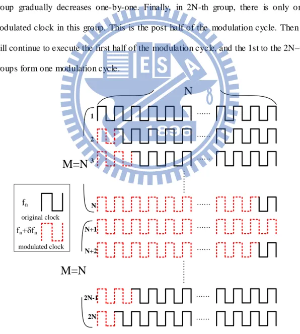
Our proposed new modulation method is shown in Fig. 3.2. We use two different
frequency clocks to achieve modulated_CLK. One is the original clock which is
CLK_REF (fn), and the other one is modulated clock with maximum frequency (fn δfn). Here, we call every N clock in Fig. 3.2 as a group and there are 2M groups in a modulation cycle. For the ease of developing the behavior, we make M=N
2nd group, only one clock is replaced by the modulated clock. In the 3rd group, two
clocks are replaced by the modulated clock. The number of modulated clocks
gradually increases one-by-one in every succeeding group. In the N-th group, N-1
original clocks are replaced by the modulated clocks. This is the first half modulation
cycle. We call this “Domino modulation method” since it like the Domino that after N
cycles, one more clock becomes modulated clock. This is the first half of the
modulation cycle. In the N+1-th group, all of the original clocks are replaced by the
modulated clocks. From N+2-th to 2N-th groups, the number of modulated clocks in a
group gradually decreases one-by-one. Finally, in 2N-th group, there is only one
modulated clock in this group. This is the post half of the modulation cycle. Then it
will continue to execute the first half of the modulation cycle, and the 1st to the 2N–th
groups form one modulation cycle.
M=N
M=N
… … … …… …… …… …… …… …… …… …… … … …N
fn fn+δfn original clock modulated clock 1 2 3 N N+1 N+2 2N-1 2NWe can observe this modulation scheme from another point of view. We calculate
the average frequency of each group. The first group is fn. The second group is
n n
1 δ N
f f . The t hird gro up is n 2 δ n
N
f f . The a vera ge freq ue nc y o f modulated_CLK in the 1st to the N+1-th groups is from fn to fnδfn. Then, the average frequency in the N+2-th to the 2N-th group is from n N-1 δ n
N f f to n n 1 δ N
f f . The total frequency deviation is δfn. The average frequency o f modulated_CLK is from fn to fn+δfn, then to fn to form a cycle, and the increasing or decreasing step of average frequency in each group is 1 δ n
N f . This
modulation profile is a triangular function.
When the δfn is positive, the modulated_CLK will perform up spread spectrum function. Then, when the δfn is negative, the modulated_CLK will perform down spread spectrum function.
The concept of the proposed Domino modulation scheme is a little like the SSCG
of phase selection of multi-phase VCO (in chapter 2, Fig. 2.11). The phase selection
modulation uses phase selection to subtract a phase from the VCO clock and the
generated CLK_DIV is a modulated_CLK. The PFD will find out t he difference
between CLK_DIV and CLK_REF. Then, Charge Pump will generate extra current to
change the voltage control node of VCO, the n frequency of VCO will change. On the
contrary, we use CLK_REF to subtract or add a phase to generate modulated_CLK
which is the output of AD-SSCG. and the frequency of CLK_DIV is fixed. Then, the
PFD will find out the difference between modulated_CLK and CLK_DIV, and finally
VCO will also achieve spread spectrum function. When the AD-SSCG block turn on
the spread spectrum function to generate modulated_CLK, PLL will track the
modulated_CLK. For example, when the division ratio is 12, and modulated
modulated_CLK is 100MHz with 0.5% frequency deviation and 30KHz modulation
frequency. The PLL will have 0.5% frequency deviation with 30KHz modulation
frequency but the frequency is 1.2GHz.
Finally, the proposed Domino modulation scheme relaxes the requirement of delay
BUF as compared with [12]. For example, if we design a 100MHz modulated_CLK
with 0.5% frequency deviation. The required delay BUF based on paper [12]
modulation is 8.3ps. However, the required delay BUF based on our Domino
modulation method is just 50ps
3.3 The Design of the Domino AD-SSCG
3.3.1 The Design of Modulated Clock
In this section, we will generate the modulated clock that we need in Domino
modulation method. In all digital circuit approach, the simple method to adjust the
width of clock is phase switching. So we need to design a multi-phase delay line. We
connect delay BUF to perform a DDLi (Digital Delay Line) as shows in Fig. 3.3. The
delay time of every delay BUF isTBUF.
Fig. 3.3 Digital Delay Line (DDLi)
In order to have up and down spread spectrum function, we need two kinds of
modulated clocks. In the following content, we discuss how to complete these two
modulation clocks which have wider and narrower period.
Case 1: The modulated clock with wider period
has different phase. Every node has a TBUF timing difference as shown in Fig. 3.3.
We connect 8 nodes to a 8-1 MUX, and we assume the delay time of the 8-1 MUX is
zero. In case 1, the phase selection starts at phase 1, and the direction of phase
switching is from phase 1 to phase 8. The timing of phase switching is that when we
find out a rising or a falling edge at present node, we will switch to next phase. As
shown in Fig. 3.4, the thick line is our phase selection path. After 7 switching times,
we can get modulated clock with wider period. The wider modulated clock is the
summation of thick line of as shown in Fig. 3.4.
Fig. 3.4 Modulated clock with wider period
There is a design consideration. Because the phase switching is from a “leading
phase” to a “lagging phase”, the instant phase switching after finding out a rising or a falling edge will generate glitch. As shown in Fig. 3.4 when we find out a rising or
falling edge, we need to delay TEXTRA to switch to next phase to avoid glitch. The glitch will not happen when TEXTRA is larger than TBUF.
Case 2: The modulation clock with narrower period
In case 2, the phase selection starts at the phase 8. And the direction of phase
switching is from phase 8 to phase 1. In the same way, when we find out a rising or a
falling edge, we switch to next phase. There is no glitch in this case because the phase
switching is from “lagging phase” to “leading phase”. As shown in Fig. 3.5, the coarse
line is our phase selection path. After 7 switching times, we can get modulated clock
wit h nar rowe r per iod. The mod ula ted c lock is t he s umma t io n o f t hick
line as shown in Fig. 3.5.
The modulated clock can be generated by phase switching. When we design case 1,
we still need to avoid occurring glitch. However, we need a lot of modulated clock in
the procedure of one cycle of Domino modulation method. It means we need infinite
phase to let us have next phase to switch continuously. In order to generate infinite
phase, we connect infinite BUFs to complete a DDLi. This implementation method of
DDLi is not practicable on chip, so we need solve this proble m. We adopt the idea
from paper [12], and discuss this structure in next section.
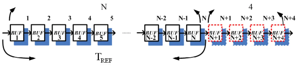
3.3.2 The Solution to Overcome Infinite Digital Delay Line
A DDLi with infinite delay is not a practical way to implement on chip. Based on
paper [12], there is a method to achieve the required DDLi. We also use this method
to implement our AD-SSCG. Firstly, we connect N BUFs for first part of DDLi and
the delay length is TCLK_REF. TCLK_REFis a period of CLK_REF, that is, the input
clock of AD-SSCG. Then, the second part of the DDLi is just several BUFs. We
connect these two parts to form complete DDLi. Thus, the delay length of the DDLi is
little more than one period (TCLK_REF). The delay of each BUF is TCLK_REF N . Fig.
3.6 shows the DDLi we describe. Here, we use 4 extra BUFs for the second part of
DDLi as an example to explain the behavior.
Fig. 3.6 The DDLi with delay time which is little more than one period
wider modulated clock. In this mode, the direction of phase switching is from left to
right. We assume that we start at phase 1. After many times of phase switching, when
we switch to phase N+4, that is, the last phase of DDLi. We have no phase to switch.
However, the designed DDLi is little more than one period of CLK_REF, there will be
two clock rising edges on the DDLi at the same time as shown in Fig. 3.7 (a). The
“next clock” will appear at phase 4 and the distance between “present clock” and “next clock” is TREF. The “present clock” can be replaced by the “next clock”. We can treat “next clock” as “present clock” with different position. Right now, the
switching phase is changed from N+4 to 4, and we have next phase to switch. The
position of phase selection is from the end of the DDLi to the head of the DDLi.
In the same concept, when we operate AD-SSCG in up spread spectrum mode,
we need to generate narrower modulated clock. In this mode, the direction of phase
switching is from right to left. We assume that we start at phase N+4 and the phase 1
is the last phase to switch. After N+3 times of phase switching, the phase 1 is selected,
and there is no phase to switch. However, we will find that another clock rising edge
appears on the DDLi at phase N+1 as shown in Fig. 3.7 (b). The distance between
“present clock” and “previous clock” is also TCLK_REF. We replace “previous clock ”
to “present clock”. Right now, the switching phase is changed from phase 1 to phase
N+1, and we have next phase to switch. The position of phase selection is from the
head of the DDLi to the end of the DDLi.
We summarize the concept of the procedure. In normal condition, that is we have
phase to switch, we just switch to next phase. However, in no switching phase
condition, we will find another clock rising edge on special designed DDLi. We can
detect the position of another clock rising edge, and switch to the position of new
Fig. 3.7 (a) “next clock” and “present clock” on DDLi (b) “present clock” and “previous clock” on DDLi
In order to find another clock rising edge, we need a circuit to do the action. We
can use DFFs to detect the rising edge. As shown in Fig. 3.8, DFFs are connected to
BUFs which locates at two sides of the delay line. The D input of DFFs is connected
to the output of BUFs. We can use the output of the selected phase as the clock of
DFFs. In Fig. 3.8, the selected phase is N. In the situation of no phase to switch, the
new clock rising edge will appear in left or right side of DDLi. So we add extra
DFFs only at two sides of DDLi.
3.3.3 The Dummy Delay Line Structure
The DDLi originally has two functions. One is to be used as a multi-phase DDLi
to execute phase switch, and the other one is providing edge detection circuit. Here,
we separate these two functions into two parts as shown in Fig. 3.9. Because (1) if the
nodes of DDLi connect too many circuits, the required delay of TBUF isn‟t easy to
complete. In practical circuit, each node of DDLi also will connect to a (N+4)-to-1
MUX. We don‟t want DFFs to increase loading. Because the detection function is
only used when there is no phase to switch, the detection circuit of DDLi can be
separated. And the CLK_REF only passes through the dummy DDLi used for
detection circuit when we require. (2) It can save power consumption. Because of
above two reasons, we adopt DDLi and dummy DDLi structure. The DFFs which are
connected to two sides of dummy DDLi are the edge detection circuit. The left side
DFFs are designed for down spread spectrum, and the right side DFFs are for up
spread spectrum. The dummy DDLi is only used when there is no phase to switch. So,
we will design a power saving mechanism for dummy DDLi to decide the turn on
t i me o f d u m m y D D L i. I n no r ma l c o nd i t io n, C LK _ R EF w i l l no t
pass through dummy DDLi.
Fig. 3.9 has one problem due to unbalanced loading. The delay BUF of dummy
DDLi should be the same as DDLi. However, the output loading of each delay BUF is
not the same on the dummy DDLi due some nodes are connected to DFFs. It will
cause the delay time of each BUF is not uniform. In order to solve problem of unequal
output loading, Fig. 3.10 is our solution. Each delay BUF connects to two series
“INV”. Because each delay BUF has the same loading, the delay of each BUF is uniform.
Fig. 3.10 DDLi and dummy DDLi with uniform delay BUF
3.4 The Behavior of Domino AD-SSCG
In this section, we will analyze the behavior for our AD-SSCG structure. Basically,
we call the input reference clock of PLL as CLK_REF. This AD-SSCG can be
designed for different specifications. There are three main parameters that we can
decide. They are (1) frequency of modulated_CLK, (2) modulation frequency, and
Recalling Fig 3.2 in section 3.2, our Domino modulatio n method has parameter
“N” and “M”. It will decide how many clocks in one time modulation. Here, we set parameter “M” is equal to “N ” to achieve optimized EMI reduction, the reason will be
discussed in section 3.7. The numbers of clocks in one time modulation is (2×N)×N.
In the formula, we define the parameters as follows fCLK_REF is the frequency of CLK_REF, is frequency deviation in ppm, and f is modulation frequency. m
Firstly, we need to estimate how many clocks in one period of modulation cycle.
The average frequency of modulated_CLK is CLK_REF 1
2 f (1+ δ)( max min avg f +f 2 f ).
The time of one period modulation is1/fm. The numbers of clocks (N ) in one C
m 1/f period is C m C L K _ R E F m C L K _ R E F T h e t i m e o f o n e p e r o i d m o d u a l t i o n N T h e a v e r a g e p e r i o d o f m o d u a l t e d _ C L K 1 / f 1 δ = f ( 1 + ) δ f 2 1/f (1+ ) 2 (3.4)
Secondly, The numbers of clocks (Nc) in one period of modulation is (2×N)×N.
C
N =(2 N) N (3.5) Let equation (3.4) is equal to equation (3.5), and then we can derive the parameter N.
For example, our AD-SSCG is designed to meet SATA-2 specification. The
frequency modulation is 30KHz to 33KHz. The frequency deviation is 5000ppm, and
it is down spread mode. The frequency of CLK_REF and modulaied_CLK is
100MHz and 99.5MHz respectively. We use the middle value of modulation
frequency which is 31.5KHz. We decide these parameters in equation (3.4) and (3.5),
3.5 Specifications of Domino AD-SSCG
Our goal is to generate a 100MHz modulated_CLK with 5000ppm frequency
deviation. We use 50ps TBUF to construct the DDLi. Besides 5000ppm frequency
deviation, we can also achieve 10000ppm and 15000ppm frequency deviation. The
method of implementation is that the amount of phase switching is 2 and 3, it will
make the effective TBUF is 100ps and 150ps. There are two kinds of modulated
clocks which are narrower and wider modulated clocks in our Domino modulation
method. So, we have up and down spread spectrum mode. Besides spread spectrum
modes, AD-SSCG can also be operated in non-spread spectrum mode by fixing the
phase of DDLi. The DDLi can be regarded as a delay cell. The output wave form of
AD-SSCG is the same as CLK_REF.
To summarize, there are totally 7 modes in the proposed Domino AD-SSCG as
shown in Table 3.2.
Table 3.2 The specification of the proposed Domino AD-SSCG
Frequency of modulated_CLK
Spread spectrum mo de Frequency deviation
100MHz down 5000ppm 100MHz down 10000ppm 100MHz down 15000ppm 100MHz up 5000ppm 100MHz up 10000ppm 100MHz up 15000ppm 100MHz non 0ppm
3.6 The Behavioral Simulations of AD-SSCG and 1.2GHz PLL
3.6.1 Behavioral Model of AD-SSCG
AD-SSCG generates modulated_CLK as the CLK_REF of PLL and Fig. 3.11 (a)
is an overall model. Fig 3.11 (b) is AD-SSCG model.
Fig. 3.11 (a) Simulink model of AD-SSCG and PLL (b) Simulink model of AD-SSCG
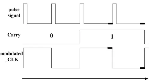
We introduce the basic mechanism of AD-SSCG model. The “Pulse Generator”
generates a pulse signal, and this pulse signal will go into the “Close-Loop Delay
Line”. The delay time of “Close-Loop Delay Line” is half period of CLK_REF. The
“Div-2” will be triggered two times by pulse signal, and generates a clock whose period is TCLK_REF as shown in Fig. 3.12. We can adjust the delay t ime o f
“Close-Loop Delay Line” block to generate wider or narrower modulated clock The “2-1 MUX” in “Close-Loop Delay Line” provides two different paths which have different delay time. When “Carry” of Delta-Sigma modulator is “0”, the pulse signal
will run the original path whose delay time is TCLK_REF/2 in “Close-Loop Delay
Line”. But when “Carry” of Delta-Sigma modulator is “1”, the pulse signal will run
anther path which is “Path2” of “2-1 MUX”, and the delay time is TCLK_REF/2 +TMUX. If the additional TMUX is positive, the delay time of “Close-Loop Delay Line” is increased to generate wider modulated clock. And if the additional TMUX is negative, the delay time of “Close- Loop Delay Line” is decreased to generate narrower
modulated clock. Fig. 3.13 shows modulated_CLK with one wider modulated clock
when “Carry” is “0” and “1”.
Fig. 3.13 The time diagram of modulated_CLK when “Carry=0 and 1”
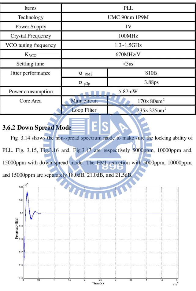
The parameters of PLL are provided by out previous design [13]. Table 3.3 shows
all the parameters we use to do the simulation. The key specifications of PLL also
listed in Table 3.3.
Table 3.3-1 The parameters of 1.2GHz PLL [13]
KVCO 700MHz/V Ip 50 uA loop filter parameters C1 70pf C2 4.6pf R1 4.5kΩ R2 1.8 kΩ C3 1.8pf N(divider ratio) 12 Input Frequency 100MHz Output Frequency 1.2GHz
Table3.3-2 The simulation results of 1.2GHz PLL [13]
Items PLL
Technology UMC 90nm 1P9M
Power Supply 1V
Crystal Frequency 100MHz
VCO tuning frequency 1.3~1.5GHz
KVCO 670MHz/V
Settling time <3us
Jitter performance σ RMS 810fs
σ p2p 3.88ps
Power consumption 5.87mW
Core Area Main circuit 2
80um 170 Loop Filter 2 um 325 235
3.6.2 Down Spread Mode
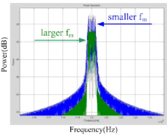
Fig. 3.14 shows the non-spread spectrum mode to make sure the locking ability of
PLL. Fig. 3.15, Fig.3.16 and, Fig.3.17 are respectively 5000ppm, 10000ppm and,
15000ppm with down spread mode. The EMI reduction with 5000ppm, 10000ppm,
and 15000ppm are separately 18.0dB, 21.0dB, and 21.5dB.
Fig. 3.15 (a) Frequency of PLL with 5000ppm and down mode (b) Spectrum of PLL with 5000ppm and down mode
Fig. 3.16 (a) Frequency of PLL with 10000ppm and down mode (b) Spectrum of PLL with 10000ppm and down mode
Fig. 3.17 (a) Frequency of PLL with 15000ppm and down mode (b) Spectrum of PLL with 15000ppm and down mode
3.6.3 Up Spread Mode
Fig. 3.18, Fig.3.19 and, Fig.3.20 are respectively 5000ppm, 10000ppm and,
15000ppm with up spread mode. The EMI reduction with 5000ppm, 10000ppm, and
15000ppm are respectively 18.1dB, 20.0dB, and 21.7dB.
Fig. 3.18 (a) Frequency of PLL with 5000ppm and up mode (b) Spectrum of PLL with 5000ppm and up mode
Fig. 3.19 (a) Frequency of PLL with 10000ppm and up mode (b) Spectrum of PLL with 10000ppm and up mode
Fig. 3.20 (a) Frequency of PLL with 15000ppm and up mode (b) Spectrum of PLL with 15000ppm and up mode
3.7 The Parameters Optimization of Domino AD-SSCG
In this section, we will discuss the reason that we set parameter “M=N” to achieve
optimized EMI reduction. Here, N defines how many clock in a group, and M defines
how many groups in the half of the modulation cycle. We will discuss the condition of
that when (1) “N=M”, (2)”N>M”, and (3) “N<M”. Then, we will find the sequence of (2) and (3) will be the same. So, we just compare the condition of N=M and N>M. We
will show a simple example when N is equal to different M, and we will get rough
understanding of different modulation scheme. Then, we use simulink model to verify
our thinking to make sure the “N=M” is the best choice for this modulation method. Our modulat ion method is that we use two kinds of clock to generate
modulated_CLK. The first group of all clocks is derived from CLK_REF. And when
the modulated_CLK has maximum frequency deviation, all clocks in that group is
replaced by modulated clocks. The average frequency of that group isfn δfn. The modulation method of (a) “N<M”, (b)”N=M”, and (c) “N>M” is shown in Fig. 3.21.
We assume N×M=16 to simply the plot. Then, we combine the first four rows and the
second four rows together of modulatio n scheme (a), and the sequence of
modulated_CLK is shown in Fig. 3.22. It will shows that the modulation scheme (a)
and (c) have one same feature of that there are four clocks will be replaced in the first
group and eight clocks will be replaced in the second group, but the modulated clocks
will appear at different positions between (a) and (c). But when we implement the
AD-SSCG, we will use 1st-ΣΔ modulator to randomize the modulated clock. Thus, the
modulated_CLK of (a) and (c) will be the same, that is, the modulated clocks will
appear in the same positions. So, we only need to compare the modulation scheme
Fig. 3.21 The modulation scheme of different N and M. (a) N=2 M=8 (N<M) (b) N=4 M=4 (N=M) (c)N=8 M=2 (N>M)
Fig. 3.22 Re-combination of modulation_CLK of (a) N=2 M=8.
Here, we assume N×M =64 to show three different modulation methods. In our
AD-SSCG, the “N×M =1600”, it is difficult to explain the behavior with different
modulation methods. So we set N×M =64 as a simple example to explain here. They
are respectively (a) N=M=8, (b) N=16 M=4, and (c) N=32 M=2 as shown in Fig. 3.23.
We can observe the average frequency of the first group of modulation scheme (a) is
n n
1 f δf
8
, then the second group is n n
2 f δf
8
frequency of the first group of modulation scheme (b) is fn 1δfn 4
, then the second is fn 2δfn
4
, and so on. We observe the average frequency of modulation scheme (c) the first group is fn 1δfn
2
, and then the second group is fn 2δfn 2
. The difference of modulation scheme is that the step numbers in frequency deviation. If there are
more steps, the modulation profile will be more like ideal triangular profile. When
PLL tracks the modulated_CLK, the spread frequency of PLL will be similar to ideal
triangular profile. The peak power of PLL will be dissipated effectively on the spread
spectrum bandwidth. Here, we think when “N=M” will be the best choice for EMI reduction because the “N=M” modulation scheme have the most steps in maximum
frequency deviation. The next paragraph will use simulink model to verify further.
Fig. 3.23 The modulation scheme of assuming N×M =64. (b) N=8 M=8 (b) N=16 M=4 (c)N=32 M=2
model of AD-SSCG and PLL in section 3.6 but with different setting of parameters N
and M. In this simulation, AD-SSCG is operated in down spread mode with
10000ppm frequency deviation. In our design, “N×M = 1600”, and three kinds of modulation scheme are used respectively (a) N=M=40, (b) N=80 M=20, and (c)
N=160 M=10. Firstly, Fig. 3.24 shows modulation profile (a) is better than (b).
Moreover, in the modulation scheme of (c), the triangular modulation profile is
distorted severely because the steps of numbers in frequency deviation are not enough.
Secondly, the EMI reduction of these three schemes is shown in Fig. 3.25, they are
respectively (a) 21.5dB, (b) 21.5dB, and (c) 18.5dB. According to the verification of
simulink model, the parameter of “N”and ”M” in the proposed Domino modulation method should be the same to achieve the optimized EMI reduction.
Fig. 3.24 Frequency of PLL with down spread mode and 10000ppm frequency deviation (a) N=M=40 (b) N=80 M=20 (c) N=160 M=10
![Fig. 2.1 FFC EMI peak limit [1]](https://thumb-ap.123doks.com/thumbv2/9libinfo/8463831.183284/20.893.140.765.443.1056/fig-ffc-emi-peak-limit.webp)
![Table 2.1 SATA-2 specifications [2]](https://thumb-ap.123doks.com/thumbv2/9libinfo/8463831.183284/21.893.128.750.349.1048/table-sata-specifications.webp)
![Fig. 3.1 The modulation method of paper [12]](https://thumb-ap.123doks.com/thumbv2/9libinfo/8463831.183284/33.893.136.766.445.1110/fig-modulation-method-paper.webp)