應用於平台式晶片系統之溫度認知功率管理的軟體矽智財設計
59
0
0
全文
(2) A Thermal-Aware Power Management Soft-IP for Platform-based SoC Designs Student. Chin-Hung Chan. Advisor. Dr. Herming Chiueh. A Thesis Submitted to Department of Communication Engineering College of Electrical Engineering and Computer Science National Chiao Tung University in Partial Fulfillment of the Requirements for the Degree of Master of Science in Communication Engineering July 2004 Hsinchu, Taiwan.
(3) (Platform-Based SoC Design) (Thermal-Aware Power Management Soft-IP Design). TSMC 0.25um 1P5M CMOS [1] (Prototype Soft-IP). i.
(4) A Thermal-Aware Power Management Soft-IP for Platform-based SoC Designs Student: Chin-Hung Chan. Advisor: Dr. Herming Chiueh. Department of Communication Engineering National Chiao Tung University Hsinchu, Taiwan. Abstract A novel thermal-aware power management (TAPM) Software Intellectual Property (Soft-IP) for modern platform-based SoC designs is presented in this thesis. This research proposes a system-level architecture of thermal-aware power management, which includes a Power Management Bus (PMB), TAPM Soft-IP and interface circuitry for proposed PMB. Each component of proposed design is encapsulated to a Soft-IP. With above design, system architects are able to incorporate on-chip power-controls and sensors to achieve nominal power dissipation and ensure the targeting system working within specification. The design yields intricate control and optimal management with little system overhead and minimum hardware requirements, as well as provides the flexibility to support different management schemes. The proposed system and its components are designed, implemented and verified by a prototype chip, which was fabricated in a TSMC 0.25um 1P5M standard CMOS technology through Chip Implementation Center (CIC), Taiwan [1].. ii.
(5) (CIC). SoC LAB. NSC-92-2218-E-009-014. iii.
(6) Content: …… ..................................................................................................i Abstract.. ................................................................................................ ii …… ............................................................................................... iii Chapter 1 Introduction...........................................................................1 1.1 Motivation .......................................................................................... 1 1.2 Organization ...................................................................................... 4. Chapter 2 System-Level Design .............................................................5 2.1 Thermal-Aware Power Management Systems.................................... 6 2.1.1 Basic Building Blocks .........................................................................6 2.1.2 System Architectures ...........................................................................7. 2.2 Specification of System Management Bus ....................................... 10 2.2.1 Introduction.......................................................................................10 2.2.2 Basic Bus Operations........................................................................10. Chapter 3 Implementation....................................................................15 3.1 Computer-Aided Design Flow ......................................................... 15 3.2 Thermal-Aware Power Management System Integration ................ 18 3.3 Verification with Testbench Set-up ................................................... 22 3.4 Simulation Results............................................................................ 25 3.4.1 Pre-layout Simulation of Multi-level Controller...............................25 3.4.2 Pre-layout Simulation of Thermal Management Unit.......................28 3.4.3 Pre-layout Simulation of System Management Bus ..........................35 3.4.4 Pre/Post-layout Simulation of System Integration............................40. 3.5 Circuit Summary .............................................................................. 47 iv.
(7) Chapter 4 Experimental Results ..........................................................49 4.1 Measurement Environment .............................................................. 49 4.2 Printed Circuit Board Design .......................................................... 51 4.3 Testing Results of Thermal Management Unit ................................. 53 4.4 Testing Results of Thermal-Aware Power Management Systems .... 61 4.5 Summary .......................................................................................... 69. Chapter 5 Conclusion & Future Works...............................................71 Bibliography: ........................................................................................74 Appendix A: The Defined Read/Write Commands for TMU..............76 Appendix B: Configuration & Report Registers Assignments ...........77. v.
(8) List of Figures: Figure 1.1 Proposed Architecture of TAPM System ...................................................................3 Figure 2.1.1 Building Blocks of TAPM.......................................................................................6 Figure 2.1.2 Detailed Block Diagram of TAPM .........................................................................8 Figure 2.1.3 TAPM System Operation........................................................................................9 Figure 2.2.1 Generic Transaction Diagram .............................................................................11 Figure 2.2.2 START and STOP Conditions...............................................................................11 Figure 2.2.3 SMBus Byte Format .............................................................................................12 Figure 2.2.4 ACK and NACK Signaling of SMBus...................................................................13 Figure 2.2.5 Write/Read Word/Byte Protocol ...........................................................................14 Figure 3.1.1 Cell-Based Design Flow ......................................................................................17 Figure 3.2.1 Schematic Circuit.................................................................................................19 Figure 3.2.2 Top Module ..........................................................................................................20 Figure 3.3.1 Testbench of MLC Set-up .....................................................................................23 Figure 3.3.2 Testbench of TMU Set-up.....................................................................................23 Figure 3.3.3 Testbench of SMBus Set-up ..................................................................................24 Figure 3.3.4 Testbench of TAPM Set-up ...................................................................................24 Figure 3.4.1 Pre-Layout Simulation of MLC............................................................................27 Figure 3.4.2 Pre-Layout Simulation of Write Commands for TMU .........................................33 Figure 3.4.3 Pre-Layout Simulation of Read Commands for TMU..........................................34 Figure 3.4.4 Pre-Layout Simulation of Write Protocol for SMBus...........................................38 Figure 3.4.5 Pre-Layout Simulation of Read Protocol for SMBus ...........................................39 Figure 3.4.6 Pre/Post-Layout Simulation of TAPM..................................................................43 Figure 3.4.7 Zoom in Sensors Firstly Change in Figure 3.4.5.................................................44. vi.
(9) Figure 3.4.8 Zoom in Sensors Secondly Change in Figure 3.4.5 .............................................45 Figure 3.4.9 Zoom in Sensors Thirdly Change in Figure 3.4.5 ................................................46 Figure 3.4.1 TAPM Chip Layout ..............................................................................................48 Figure 4.1.1 Testing Set-Up......................................................................................................50 Figure 4.1.2 Photograph of Testing Environment ....................................................................50 Figure 4.2.1 PCB Circuit Implementation................................................................................51 Figure 4.2.2 Photograph of Taped-out Chip on PCB...............................................................52 Figure 4.3.1 Testing TMU & MLC Block .................................................................................53 Figure 4.3.2 Testing Controller Registers by 00h Pattern........................................................54 Figure 4.3.3 Testing Controller Registers by 55h Pattern........................................................54 Figure 4.3.4 Testing Controller Registers by AAh Pattern .......................................................54 Figure 4.3.5 Testing Controller Registers by FFh Pattern.......................................................55 Figure 4.3.6 Testing Controller Registers by Different Patterns ..............................................55 Figure 4.3.7 Testing Temperature Registers by 00h Pattern ....................................................55 Figure 4.3.8 Testing Temperature Registers by 55h Pattern ....................................................55 Figure 4.3.9 Testing Temperature Registers by AAh Pattern....................................................56 Figure 4.3.10 Testing Temperature Registers by FFh Pattern..................................................56 Figure 4.3.11 Testing Temperature Registers by Different Patterns .........................................56 Figure 4.3.12 Testing (Offset) Threshold Registers by 00h Pattern .........................................57 Figure 4.3.13 Testing (Offset) Threshold Registers by 55h Pattern .........................................57 Figure 4.3.14 Testing (Offset) Threshold Registers by AAh Pattern.........................................57 Figure 4.3.15 Testing (Offset) Threshold Registers by FFh Pattern.........................................57 Figure 4.3.16 Testing (Offset) High/Low Threshold Registers by Different Patterns...............58 Figure 4.3.17 Testing Interrupt and Offset Interrupt Functions...............................................60 Figure 4.4.1 Testing TAPM Block.............................................................................................61 Figure 4.4.2 Testing Controller Register 0 by SMBus (Test Pattern AAh) ...............................63 vii.
(10) Figure 4.4.3 Testing Controller Register 1 by SMBus (Test Pattern AAh) ...............................64 Figure 4.4.4 Testing Controller Register 2 by SMBus (Test Pattern AAh) ...............................64 Figure 4.4.5 Testing Controller Register 3 by SMBus (Test Pattern AAh) ...............................64 Figure 4.4.6 Testing Threshold Register 0 by SMBus (Test Pattern 55h & AAh) .....................64 Figure 4.4.7 Testing Threshold Register 1 by SMBus (Test Pattern 55h & AAh) .....................65 Figure 4.4.8 Testing Threshold Register 2 by SMBus (Test Pattern 55h & AAh) .....................65 Figure 4.4.9 Testing Threshold Register 3 by SMBus (Test Pattern 55h & AAh) .....................65 Figure 4.4.10 Testing Offset Threshold Register by SMBus (Test Pattern 55h & AAh)............65 Figure 4.4.11 Testing Temperature Register 0/3 by SMBus (Test Pattern 80h/FFh) ................66 Figure 4.4.12 Testing Temperature Register 1/2 by SMBus (Test Pattern C0h/D5h) ...............66 Figure 4.4.13 Testing Interrupt and Offset Interrupt by SMBus...............................................67 Figure 4.4.14 Zoom in Sensors Firstly Change in Figure 4.4.13.............................................67 Figure 4.4.15 Zoom in Sensors Secondly Change in Figure 4.4.13 .........................................68 Figure 4.4.16 Zoom in Sensors Thirdly Change in Figure 4.4.13 ............................................68 Figure 4.5.1 Die Microphotograph ..........................................................................................70 Figure 5.1.1 Building Blocks of Temperature Sensor with TAPM ............................................72 Figure 5.1.2 Building Blocks of Voltage Island with TAPM .....................................................73. viii.
(11) List of Tables: Table 3.2.1 Output Signal Description of Top Module .............................................................20 Table 3.2.2 Input Signal Description of Top Module................................................................21 Table 3.4.1 Signal Description of I/O Ports for Figure 3.4.1...................................................25 Table 3.4.2 Signal Description of I/O Ports for Figure 3.4.2 and 3.4.3...................................32 Table 3.4.3 Signal Description of I/O Ports for Figure 3.4.4 and 3.4.5...................................37 Table 3.4.4 Signal Description of I/O Ports for Figure 3.4.6~9...............................................42 Table 3.4.1 Circuit Summaries .................................................................................................48 Table 4.4.1 Expositions for Figure 4.4.2~10 ............................................................................63 Table 4.5.1 Actual System Perfromance ...................................................................................70. ix.
(12) __________________________________ Chapter 1 Introduction __________________________________ 1.1 Motivation Modern semiconductor technologies enable the integration of different components from an on-board system to a single chip using reliable design tools and methodologies. Different novel material and process technologies, including embedded memories, embedded processors, copper interconnect, low-k dielectric material and high-Q passive component, supply low-noise and low-resistance interconnects for mixed-signal design and high speed circuit design. The evolution of recent Electronics Design Automation (EDA) tools and design methodologies such as hardware/software co-design, code coverage analysis as well as high-level synthesis and language [2], help designers to verify and implement their project in a short time. Thus, the design productivity is increased, and the System-on-Chip (SoC) design is no longer an unreachable goal for designers. As the whole systems merge into a single chip, the total area and circuit complexity of a SoC design increase dramatically. The time-to-market pressure and integration of such a complex system have brought different design and verification methodologies to increase the design efficiency. Thus, IP-based and Platform-based SoC design [3] is proposed, which are solutions for these challenges of SoC design. By using such methodologies, the concept of utilizing designed Intellectual Property (IP) cores is widely used to achieve the performance and function requirements of a 1.
(13) targeted SoC. As circuit density and operation frequency of the SoC design increased, more power dissipated on a single chip and more heat generated on a single dies. The local heated up seriously impacts the system performance. Thus, how to quickly dissipate the heat has become an important research topic in recent years. The previous researches have proposed the dynamic thermal management system (TMS) [4-6] to solve the thermal problem on SoC design. In this research, a “Soft-IP” is designed for Thermal-Aware Power Management system (TAPM) in order to integrate with targeting system. The proposed TAPM is designed as a synthesizable module in a hardware description language such as Verilog or VHDL and can be easily transferred to different manufacturing technologies [7]. The advantage provides a faster implementation for new designs. Besides the TAPM Soft-IP, an interface module is designed to provide the communication mechanism between TAPM and other IPs on targeting SoC bus. However, in this design, a controlling bus which adopts the System Management Bus (SMBus) standard [8] is also proposed. In Figure 1, the processor, TAPM and other functional units are connected by high speed bus, such as AMBA [9], IBM core connect [10] and MIPS’ EC bus [11]. In addition, each IPs is connected by the SMBus to communicate actively with TAPM to implement the system-level power management. The interface module for each IPs on the system is also provided as a Soft-IP in proposed design. The purpose of such set-up is to offer a separate power management bus for the whole system. Such bus is necessary since the performance of system bus can be seriously decreased because active thermal/power management often comes with a lot of interrupts and power setting commands. Such set-up does not require a high speed communication 2.
(14) between TAPM and different IPs, but the frequent interrupts will hurt the performance of most SoC on-chip buses. In the mean time, most on-chip buses are designed to provide a relatively higher data-bandwidth compared with peripheral buses and controlling buses, which means TAPM might not take charge of the buses while the critical thermal or power failure are happening. Thus, the proposed design utilized a separate power management bus in a lower clock-rate (compared with the platform) to delicately control all the power/thermal commands and events. To solve above problems and fulfill such requirements, the SMBus was chosen since it provided a 2~3 wires connection with a relative lower clock rate which implied a very tiny overhead in terms of power and area for targeting SoC designs. This thesis proposed a thermal aware architecture for SoC designs which includes the bus architecture, SMBus interface and TAPM micro-architecture. These units are encapsulated to Soft-IPs, and are fabricated and verified in a prototype chip using TSMC 0.25um 1P5M standard CMOS process.. Figure 1.1 Proposed Architecture of TAPM System 3.
(15) 1.2 Organization In Chapter 1, the overview of SoC design trends and platform-based SoC designs from IP viewpoints are described. From thermal/power impact on SoC designs, the concept of TAPM Soft-IP is proposed for this catastrophe. In Chapter 2, the system-level design issues are mentioned. The functional units and architecture of TAPM are addressed and illustrated, which is followed by introduction of SMBus. In Chapter 3, the design flow, circuitry integration, and simulations are shown. Finally, the circuit summary of TAPM is presented. In Chapter 4, the environment of measurement set-up is shown, and the printed circuit board (PCB) design issues are proposed and implemented. The experimental results of taped-out chip are presented. In Chapter 5, this proposed design is concluded, which is followed by discussing for future works.. 4.
(16) __________________________________ Chapter 2 System-Level Design __________________________________ In this chapter, the system-level design of TAPM is shown. Based on the proposed architecture of TAPM system in Figure 1.1 in previous chapter, the backup transmission bus, SMBus, was implemented and designed as modules [12], which is directly adopted by this design because it’s characteristic provides a control for system and power management related tasks. In addition, for die size and power density increasing in the SoC design, the on-chip temperature gradient becomes a major problem for system stability. The feature of TAPM must deal with local overheating and offset overheating events and provided essential the multi-stage monitor for temperature variance on chips. From some compact thermal/power models to predict the thermal/power distribution on chips, TAPM can be necessarily programmed suitable critical value and decided where place the sensors on targeted system. Thus, the flexible architecture using little overhead is another consideration in order to support different thermal/power management scheme according to targeted system characteristic. In Section 2.1, the proposed architecture of TAPM is shown. The specification of SMBus is introduced in Section 2.2.. 5.
(17) 2.1 Thermal-Aware Power Management Systems 2.1.1 Basic Building Blocks The building block of a complete TAPM with the targeted SoC design is shown in Figure 2.1.1. The dotted-line defines whole system that includes Thermal Management Units (TMU), Power Control & Active Cooling Units (PC&AC), temperatures sensors, targeted systems and interfaces. The dashed-line indicates the designed TAPM IP, which includes a TMU, a PC&AC and an interface circuit (SMBus). The selections of every sub-unit design depend on the speciation of the targeting system in order to reduce the cost and complexity of final system design. The temperature sensors, TMU and PC&AC build up a feedback-loop to control and stabilize thermal events and power consumptions of targeting SoC design. The TMU can be programmed by different power management algorithms to fit the thermal/power requirements of different targeting system.. Figure 2.1.1 Building Blocks of TAPM 6.
(18) 2.1.2 System Architectures The detailed block diagram of TAPM is shown in Figure 2.1.2. The explanations of each block are described in the following paragraphs: Offset temperature threshold, temperature threshold, temperature of sensors, system reports, system configuration and driven value of controllers are individually stored in the six kinds of specified register of TMU. By using defined command through SMBus, the setting of above registers can be adjusted to optimize the different power management levels, and keep states of the targeted system within specified temperature/power range. As this Figure 2.1.2 indicates, comparators are used to compare the sensor temperature with specified threshold in order to monitor states of different location for either overheating or offset overheating. The dashed-arrows indicate the control loops of configuration registers and assigned comparators and sensors. If overheating or offset overheating happens, the interrupt generator will produce a corresponding interrupt signal to the processor. The system reports were read out from report registers of TMU through SMBus in order to understand the system situation. The Pulse-Width-Modulation (PWM) controllers are chosen as Multi-level controller in this design. Based on the previous research [13], this pure digital design yields lower cost and higher efficiency than conventional liner driven fan controllers. The total area of this design can be decreased by using less shift-register [14]. It can trigger a 256-level signal to control the cooling device or voltage regulated device, and takes one step ahead to strengthen performance of TAPM. A master interface and a slave interface of SMBus are designed. There are two wires in SMBus, and the transmission is bi-directional on SMBDAT. Originally, a tri-state buffer is necessary for the output stage, but it is difficult for designers to do timing control on this buffer. Thus, the input and output data are split into two wires. 7.
(19) The operation frequency of SMBus (SMBCLK) is from 10 to 100 KHz. The SMB clock is generated by SMB master interface. Each cycle of SMBCLK is divided into least six cycles of internal clock according to the frequency of internal clock, and this period would match the minimum high period of SMBCLK, hold time of start condition and setup time of stop condition in AC specification. The timing parameters of the master interface and slave interface can be easily set up to fit the variant clock-rate requirements for different targeting systems.. Figure 2.1.2 Detailed Block Diagram of TAPM. 8.
(20) In Figure 2.1.3, by integrating various sensors with TMU, TAPM can rigorously monitor power, thermal/power and cooling level for targeting SoC design. In addition, individually functional blocks of the SoC design can have unique power characteristics, and can be optimized based on requirement of its voltage. Thus, the voltage islands are capable of providing design leverage [15], and the regulative mechanisms of voltages can be adopted to scale voltage at any region in order to enhance power control ability of TAPM.. µP. Figure 2.1.3 TAPM System Operation. 9.
(21) 2.2 Specification of System Management Bus According to the specification version 2.0 [8], the SMBus is introduced in Section 2.2.1, and the basic data transfer and read/write protocol of the bus is presented in Section 2.2.2.. 2.2.1 Introduction The SMBus is based on the principles of operation of I2C, which was developed in the early 1980’s by Philips semiconductors, and its purposes were to provide an easy way to connect a CPU to peripheral chips. In February 1995, Intel Corporation defined the SMBus. It is widely used in personal computers and servers for low-speed system management communications. The various system components can communicate with each other or the rest of the system through SMBus that is a two-wire interface. The SMBus provides a control bus for system and power management related tasks. Due to removing the individual control lines in order to reduce pins count, a system may use SMBus to transmit messages to devices and received messages from devices instead of tripping individual control lines.. 2.2.2 Basic Bus Operations In Figure 2.2.1, the SMBus addresses are 7 binary bits long and are conventionally expressed as 4 bits followed by 3 bits followed by the letter ‘b’ which is binary format, such as “0001 110b”. These addresses occupy the high seven bits of an eight-bit field on the bus. However, the low bit of this field has other semantic meaning that is not part of a SMBus address. In this figure, the un-shaded portions are supplied by the bus master and the shaded portions are driven by the bus slave. The numbers across the top of the transaction diagram indicate the bit widths of each field. The specific SMBus START and STOP conditions are defined in Figure 2.2.2.. 10.
(22) Figure 2.2.1 Generic Transaction Diagram. Figure 2.2.2 START and STOP Conditions. The START and STOP conditions are always generated by the bus master, and its definition is described in the following paragraphs: START Condition: A HIGH to LOW transition of the SMBDAT line while SMBCLK is HIGH indicates a message START condition. After a START condition, the bus is considered to be busy. STOP Condition: A LOW to HIGH transition of the SMBDAT line while SMBCLK is HIGH defines a message STOP condition. The bus becomes idle state after certain time following by a STOP condition. In Figure 2.2.3, every byte consists of 8 bits, and each byte transferred on the bus must be followed by an acknowledge bit. In Figure 2.2.4, the positioning of acknowledge (ACK) and not acknowledge (NACK) pulses relative to other data are illustrated. The acknowledge-related clock pulse is generated by the master. The transmitter, master or slave, releases the SMBDAT line (HIGH) during the acknowledge clock cycle. In order to acknowledge a byte, the receiver must pull the 11.
(23) SMBDAT line LOW during the HIGH period of the clock pulse according to the SMBus timing specifications. A receiver that wishes to NACK a byte must let the SMBDAT line remain HIGH during the acknowledge clock pulse. A SMBus device must always acknowledge (ACK) its own address. A SMBus slave device may decide to NACK a byte other than the address byte, which described in the following paragraphs: First, the slave device is busy performing a real time task, or data requested are not available. Upon detection of the NACK condition, the master must generate a STOP condition to abort the transfer. Second, the slave device detects an invalid command or invalid data. In this case, the slave device must NACK the received byte. Upon detection of this condition, the master must generate a STOP condition and retry the transaction.. Figure 2.2.3 SMBus Byte Format. 12.
(24) Figure 2.2.4 ACK and NACK Signaling of SMBus. In Figure 2.2.5, the write/read word/byte protocol is described in the following paragraphs: After the master asserts the slave device address followed by the write bit, the device acknowledges and the master delivers the command code. The first byte of a Write Byte/Word access is the command code. The next one or two bytes are the data to be written. The slave again acknowledges before the master sends the data byte or word. The slave acknowledges each byte, and the entire transaction is finished with a STOP condition. Reading data is slightly more complicated than writing data. First, the host must write a command to the slave device. Then it must follow that command with a repeated START condition to denote a read from that device’s address. The slave then returns one or two bytes of data. Note that there is no STOP condition before the repeated START condition, and that a NACK signifies the end of the read transfer. Similarly, the entire transaction is finished with a STOP condition.. 13.
(25) Figure 2.2.5 Write/Read Word/Byte Protocol 14.
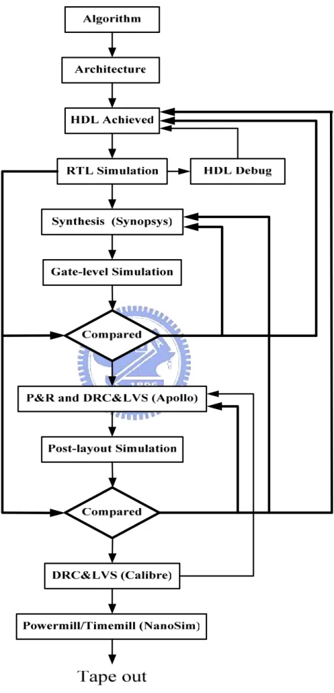
(26) __________________________________ Chapter 3 Implementation __________________________________ In this chapter, the implementation of the taped-out IP is presented. The Computer-Aided Design (CAD) flow for cell-based design is introduced in Section 3.1. The TAPM integration is shown in Section 3.2, and the verification with testbench set-up for TAPM is shown in Section 3.3. The pre-layout simulation of every component and pre/post-layout simulation of the whole system integration are shown in Section 3.4. Finally, the circuit summaries of the taped-out IP are presented in Section 3.5.. 3.1 Computer-Aided Design Flow A complete digital design flow with standard cells is shown in Figure 3.1.1. The three main Electronics Design Automation (EDA) tools are used to design this IP, one is simulator, another is synthesizer and the other is automatic placement and routing tools. Hardware Description Language (HDL), Verilog, is used to stylize proposed architecture. Each step of this design flow is introduced in the following paragraphs: First, algorithms and architectures must be decided before implementations, including selected standard interface, defined system performance and system functions. After the specification of this design was formulated, the proposed architecture is carefully delimited to several module based on individual characteristics of modules. This crucial stage for designs directly affects the signals of modules communicating with each other, and indirect determines synthesis results. 15.
(27) Second, the proposed design is stylized by Verilog language, which must be synthesizable codes. Register-Transfer-Level (RTL) simulations verify the behavioral functions of modules, which do not take timing into account, such as wire delays, gate delay and transport delay. Once RTL simulations do not match demanded functions, RTL codes must be modified and simulated again. Third, after verifications of the functions, RTL codes are synthesized by synthesizer according to select logic cells from standard cell library. Setting synthesis constraints fits requirements of system performance, and gate power, gate counts, as well as timing information between gates can be estimated from the synthesis reports. After synthesis, Gate-Level simulations consider gate timing, which verify the functions of gate-level netlist. Similarly, if simulation results do not match behavioral functions as these problems of hold time and setup time between modules, we must go back preceding stage to solve these troubles. Forth, the appropriate constrains are set to optimize the floorplanning by automatic placement and routing tools. Besides Post-layout simulations checking, another two checking is necessary. One, Layout Versus Schematic (LVS) checks the connectivity of a physical layout design to its related schematic circuit netlist. Another, Design Rule Check (DRC) checks the physical layout data against the design rules of the fabrication. Each design must follow design rule document that is golden; after checking, designers find all DRC errors out and have to modify these. Transistor-Level (Circuit-Level) simulations are essential to analyzes power and check timing. The design has gone through this cell-based design flow to produce GDSII layout file, which can be fabricated in any foundry.. 16.
(28) Figure 3.1.1 Cell-Based Design Flow 17.
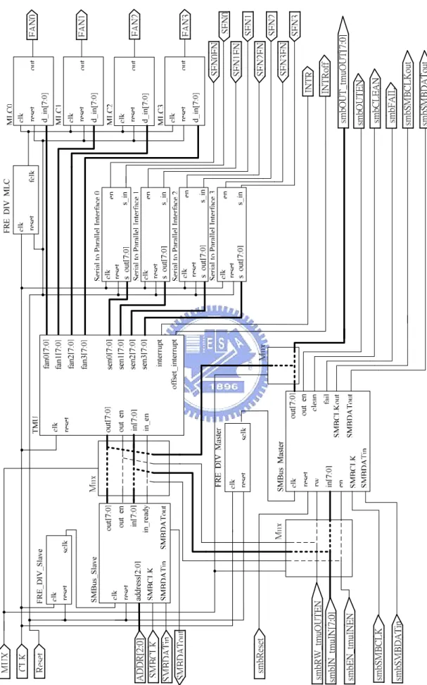
(29) 3.2 Thermal-Aware Power Management System Integration This section presents a prototype implementation of the proposed design according to cell-based design flow in the previous section, which adopts TSMC 0.25um process with the Aritsan standard cells. First, the behavioral verilog code is verified by Simulator Verilog-XL and Debugger/Checker Debussy. After the verification, this IP is synthesized by Synopsys Design Analyzer. The gate-level synthesis results are verified before Synopsys Apollo is used to place and route for the IP floorplanning, which is followed by Circuit Simulator NanoSim. This IP was fabricated in TSMC through CIC. The schematic circuit of the taped-out IP is shown in Figure 3.2.1. This IP includes a TMU, four MLCs, four serial-to-parallel interfaces of temperature sensors, a slave interface and a master interface of SMBus. Furthermore, the input clock is separated into three kinds of internal clock; one is for TMU, another is for MLC and the other is for SMBus. The serial-to-parallel interfaces of temperature sensors can reduce the Input/Output (I/O) pins and total areas of this IP since I/O pins might cause pad limited design. By integrating a master of SMBus into this IP, the transfer of SMBus can be observed between the master interface and slave interface. In addition, we also take account of the measurement for this IP in order to test TMU and TAPM individually. This approach enables us to check the functional units of this IP separately, and functional units can be selected by using a multiplexer, a “MUX” input as shown in Figure 3.2.1. The I/O ports of the top module is shown in Figure 3.2.2, and their signal description are summarizes in Table 3.2.1 and Table 3.2.2.. 18.
(30) Figure 3.2.1 Schematic Circuit 19.
(31) Figure 3.2.2 Top Module. Table 3.2.1 Output Signal Description of Top Module. Signal Description. Output Port Name. SMBDATout. Slave-to-Master bus data output (Mux=1). FAN0~FAN3. MLC0~3 output. INTR. interrupt signal due to local temperature overflow/underflow. INTRoff. offset interrupt signal due to offset temperature overflow/underflow. smbOUT_tmuOUT[7:0]. data output of master interface (Mux=1); data output data of TMU (Mux=0). smbSMBCLKout. Master-to-Slave bus clock output (Mux=1). smbSMBDATout. Master-to-Slave bus data output (Mux=1). smbCLEAN. when it’s accessed, sent data is successful, then continue to send next data (Mux=1). smbFAIL. when it’s accessed, sent data is failure, then try to send data again (Mux=1). smbOUTEN. received byte is completed, when it’s accessed (Mux=1). 20.
(32) Table 3.2.2 Input Signal Description of Top Module. Input Port Name. Signal Description. CLK. TAPM internal clock. MUX. test TAPM, when it’s “High” ; test TMU, when it’s “Low”. RESET. TAPM reset. ADDR[2:0]. address of slave interface (Mux=1). SMBCLK. Master-to-Slave bus clock (Mux=1). SMBDATin. Master-to-Slave bus data input (Mux=1). SEN0~SEN3. sensor0~3 serial input. SEN0EN~SEN3EN. sensor0~3 serial-to-parallel enable line. smbRESET. master interface reset (Mux=0). smbIN_tmuIN[7:0]. data input of master interface (Mux=1); data input of TMU (Mux=0). smbEN_tmuINEN. enable write/read protocol of master interface (Mux=1); data is written into TMU, when it’s accessed (Mux=0). smbRW_tmuOUTEN. select read/write protocol for master interface (Mux=1); data is read from TMU, when it’s accessed (Mux=0). smbSMBCLK. bus clock input of master interface (Mux=1). smbSMBDATin. Slave-to-Master bus data input (Mux=1). 21.
(33) 3.3 Verification with Testbench Set-up In this section, each modules of the TAPM is verified by individual testbench set-up. The diagram of the testbench set-up for MLC is shown in Figure 3.3.1. The function of this module must provide Pulse-Width-Modulation (PWM) control. Thus, the testbench need to access (write) variously driven value into input “D_in” in order to ensure that there are different level PWM signal from the output “OUT”. The verification of TMU module is shown in Figure 3.3.2. There is programmable block in TMU; this block must be normally accessed (write/read), so testbench includes writing data test and reading data test. Another function is interrupt generators is also checked. The local overheat and offset overheat events are utilized to trigger corresponding interrupt signal in order into verify these functions. In Figure 3.3.3, the testbench set-up of the SMBus is shown. The interactive signals between the master and slave interface of SMBus are verified, so the testbench includes write and read protocol of the specification in order to test SMBus transaction functions. The final testbench set-up is shown in Figure 3.3.4, and the three main principle of testing TAPM is described as following. One, the programmable block of TMU is accessed (write/read) by SMBus. Another, the driven value of MLC from programmable block of TMU is checked by estimating output of MLC0~3. The other, the interrupt generator is also verified in this stage. In next section, the every module and TAPM integration are simulated based on these testbench set-up diagram in this section.. 22.
(34) Figure 3.3.1 Testbench of MLC Set-up. Figure 3.3.2 Testbench of TMU Set-up. 23.
(35) Figure 3.3.3 Testbench of SMBus Set-up. Figure 3.3.4 Testbench of TAPM Set-up. 24.
(36) 3.4 Simulation Results The pre-layout simulations of MLC, TMU and SMBus are shown in Section 3.4.1, Section 3.4.2 and Section 3.4.3, respectively. Finally, the Pre/Post-layout simulations of the system integration are shown in Section 3.4.4.. 3.4.1 Pre-layout Simulation of Multi-level Controller In Figure 3.4.1, the pre-layout simulation of MLC is presented, and its I/O ports is described in Table 3.4.1. In this simulation, all of the signal value is set hexadecimal form, and the timescale unit is 100 picoseconds. According to testbench considerations of the MLC module in Section 3.3, its verification is described as following steps: Step1: drive “01H” into input “d_in[7:0]”, estimate output “out” Step2: drive “03H” into input “d_in[7:0]”, estimate output “out” Step3: drive “07H” into input “d_in[7:0]”, estimate output “out” Step4: drive “0fH” into input “d_in[7:0]”, estimate output “out” Step5: drive “1fH” into input “d_in[7:0]”, estimate output “out” Step6: drive “3fH” into input “d_in[7:0]”, estimate output “out” Step7: drive “7fH” into input “d_in[7:0]”, estimate output “out” Step8: drive “ffH” into input “d_in[7:0]”, estimate output “out”. Table 3.4.1 Signal Description of I/O Ports for Figure 3.4.1. Signal Description. I/O Ports Name. clk. MLC internal clock. reset. MLC reset. d_in[7:0]. MLC input. out. MLC PWM output. 25.
(37) The detailed explanations are that after the six input data of the “d_in” is stored in MLC at time stamps of 0.035us, 10.06us, 20.085us, 30.11us, 40.135us, 50.16us, 60.185us and 70.205us, the output “out” produces six kind outputs of the Pulse-Width-Modulation (PWM). The simulation result demonstrates that the designed MLC matches our expectation.. 26.
(38) Figure 3.4.1 Pre-Layout Simulation of MLC. 27. Cursor: 0. Marker:0. 0. 0. Delta:0. 1. x 100ps. 3. 200000. 200000. 7. f. 400000. 400000. 1f. 3f. 600000. 600000. 7f. ff. 800000. 800000.
(39) 3.4.2 Pre-layout Simulation of Thermal Management Unit The pre-layout simulations of TMU are presented in Figure 3.4.2 that is followed by Figure 3.4.3 and its I/O ports is described in Table 3.4.2. In these simulations, all of the signal value is set hexadecimal form, and the timescale unit is 100 picoseconds. The defined read/write commands of TMU is shown in Appendix A, and the detailed assignments of Configuration, Report 1 and Report 2 register are shown in Appendix B. Based on Appendix A and Appendix B, these simulation are clearly understood. The testbench considerations are explained in Section 3.3, and the verification is described as following steps: Step01: reset is accessed, all register is initialized Step02: temperature of sensor0~3 change, estimate registers “TEMP0~3[7:0]” Step03: set system configuration to “ffH”, estimate register “CONFIG[7:0]” Step04: set driven value for MLC0 to “11H”, estimate register “FAN0[7:0]” Step05: set driven value for MLC1 to “12H”, estimate register “FAN1[7:0]” Step06: set driven value for MLC2 to “13H”, estimate register “FAN2[7:0]” Step07: set driven value for MLC3 to “14H”, estimate register “FAN3[7:0]” Step08: set low/high threshold for sensor0 to “01H/15H”, estimate register “THRES0[15:0]" Step09: set low/high threshold for sensor1 to “02H/16H”, estimate register “THRES1[15:0]" Step10: set low/high threshold for sensor2 to “03H/17H”, estimate register “THRES2[15:0]" Step11: set low/high threshold for sensor3 to “04H/18H”, estimate register “THRES3[15:0]" Step12: set offset low/high threshold to “fbH/05H”, estimate register “OFFS_THRES[15:0]" 28.
(40) Step13: temperature of sensor0~3 change, estimate registers “TEMP0~3[7:0]” Step14: local overheating & offset overheating of sensor2 happen, estimate output “intr” & “intr_offs” Step15: read data from register “CONFIG[7:0]”, estimate output “OUT[7:0]” Step16: read data from register “REPORT0[15:0]”, estimate output “OUT[7:0]” Step17: read data from register “REPORT1[15:0]”, estimate output “OUT[7:0]” Step18: read data from register “FAN0[7:0]”, estimate output “OUT[7:0]” Step19: read data from register “FAN1[7:0]”, estimate output “OUT[7:0]” Step20: read data from register “FAN2[7:0]”, estimate output “OUT[7:0]” Step21: read data from register “FAN3[7:0]”, estimate output “OUT[7:0]” Step22: read data from register “TEMP0[7:0]”, estimate output “OUT[7:0]” Step23: read data from register “TEMP1[7:0]”, estimate output “OUT[7:0]” Step24: read data from register “TEMP2[7:0]”, estimate output “OUT[7:0]” Step25: read data from register “TEMP3[7:0]”, estimate output “OUT[7:0]” Step26: read data from register “THRES0[15:0]”, estimate output “OUT[7:0]” Step27: read data from register “THRES1[15:0]”, estimate output “OUT[7:0]” Step28: read data from register “THRES2[15:0]”, estimate output “OUT[7:0]” Step29: read data from register “THRES3[15:0]”, estimate output “OUT[7:0]” Step30: read data from register “OFFS_THRES[15:0]”, estimate output “OUT[7:0]” Step31: temperature of sensor 0~3 change, estimate registers “TEMP0~3[7:0]” Step32: local overheating & offset overheating of sensor3 end, estimate output “intr” & “intr_offs”. 29.
(41) The detailed explanations are shown as following two paragraphs: In Figure 3.4.2, the data is written into all of the registers of TMU with using defined command. When reset was accessed at a time stamp of 10ns, TEMP0~3 registers is initialized to “00H”; FANC0~3 registers is initialized to “7fH”; THRES0~3 registers is initialized to “3c00H” which is high threshold and low threshold; OFFS_THRES registers is initialized to “0a0aH”, offset high and low threshold are the same “0aH”; CONFIG register is initialized to “ffH”. After the “sen0~3” read serial data from time stamps of 32.3ns to 123ns, and “11H” and “13H” store in TEMP0~1 and TEMP2~3 registers. When the input “in_en” is accessed each time, the input data is being stored in specified register. With looking up Appendix A, every register be changed from initial value to assigned value, which can be carefully observed from left to right in Figure 3.4.2. Following Figure 3.4.2, in Figure 3.4.3, the data is read from all of the registers of TMU by using defined command after setting value was assigned to every register. The input “sen0~3” is changed again from time stamps of 1633.3ns to 1724.3ns. At a time stamp of 1725ns, the output “intr” and “intr_offs” is accessed to notify processor due to offset overflow/underflow and local overflow of sensor2. The local overflow is temperature of the sensor over set threshold, and the offset temperature overflow/underflow is the temperature difference between two positions over/under offset threshold. From a time stamp of 7714.3ns to 7805.3ns, the input “sen0~3” is changed. The temperature of the sensors is no longer overheating and offset overheating, so the interrupt signal and the offset interrupt signal end at a time stamp of 7806ns. When the input “out_en” is accessed each time, the output data is being read from specified registers. With looking up Appendix A, every output data come from specified register, which can be carefully observed. By analyzing the output value of Report1, Report2 and Configuration registers, the states of TMU are known 30.
(42) based on Appendix B. The two functions are confirmed by us from these simulation results. One, all registers of the designed TMU can be normally accessed and stored with using the defined commands. Another, the interrupt generator can notify the processor in time when system is overheating and offset overheating.. 31.
(43) Table 3.4.2 Signal Description of I/O Ports for Figure 3.4.2 and 3.4.3. Signal Description. I/O Ports Name. clk. TMU internal clock. reset. TMU reset. IN[7:0]. TMU input (8 bits command according to Appendix A). in_en. data write into TMU, when it’s accessed. OUT[7:0]. TMU output. out_en. data is read from TMU, when it’s accessed. sen0. sensor0 serial input. sen0_en. sensor0 serial-to-parallel enable line. sen1. sensor1 serial input. sen1_en. sensor1 serial-to-parallel enable line. sen2. sensor2 serial input. sen2_en. sensor2 serial-to-parallel enable line. sen3. sensor3 serial input. sen3_en. sensor3 serial-to-parallel enable line. TEMP0[7:0]. store temperature data of sensor0. TEMP1[7:0]. store temperature data of sensor1. TEMP2[7:0]. store temperature data of sensor2. TEMP3[7:0]. store temperature data of sensor3. FAN0[7:0]. store driven data for MLC0. FAN1[7:0]. store driven data for MLC1. FAN2[7:0]. store driven data for MLC2. FAN3[7:0]. store driven data for MLC3. THRES0[15:0]. store local threshold for sensor0. THRES1[15:0]. store local threshold for sensor1. THRES2[15:0]. store local threshold for sensor2. THRES3[15:0]. store local threshold for sensor3. OFFS_THRES[15:0] store offset threshold for sensors. intr. interrupt signal due to local temperature overflow/underflow. intr_offs. offset interrupt signal due to offset temperature overflow/underflow. REPORT0[7:0]. local overflow/underflow report for sensors. REPORT1[7:0]. offset overflow/underflow report for sensors. CONFIG[7:0]. system configuration. 32.
(44) Figure 3.4.2 Pre-Layout Simulation of Write Commands for TMU. 33. Cursor: 0. Marker:0. 0. 0. 0 0 0 0. XX. Delta:0. 7f. f. x 100ps. 7f. ff. 7f. 0. 7f. 11. 20000. 3c00. 1. 12. 3c00. 2. 5000. 3c00. 13. 3. 3c00. 14. 40000. a0a. 8 0. 0 0 ff. 3c01. 1. 11 11 13 13. 15. 9. 3c02. 11. 2. 16. 12. 10000. 13. a. 60000. 3c03. 14. 3. 1501. 17. b. 3c04. 1602. 4. 1703. 18. c. 80000. 1804 afb. fb. 15000. 5fb. 5.
(45) Figure 3.4.3 Pre-Layout Simulation of Read Commands for TMU. 34. Cursor: 0. Marker:0. *. *. 50. 0. 20000. 4. 11. 12. 81. 13. 82. 14. 83. 16. 85. 40000. 15. 84. 20 450 ff. 0. 80. 0 0. 20. 8e. 15 16 1f 17 11 12 13 14 1501 1602 1703 1804 5fb. ff. 0. 8d. 40000. 11 11 13 13. 8f. 20000. x 100ps. 5. Delta:0. 1f. 86. 17. 87. 1. 88. 15. 60000. 2. 89. 60000. 16. 3. 8a. 17. 4. 8b. 80000. 18. fb. 8c. 5. 0 0. 8 8 9 9.
(46) 3.4.3 Pre-layout Simulation of System Management Bus The pre-layout simulation of SMBus is presented in Figure 3.4.4 which is followed by Figure 3.4.5, and its I/O ports is described in Table 3.4.3. In these simulations, all of the signal value is set hexadecimal form, and the timescale unit is 10 nanoseconds. The address of the slave interface is assigned to “04H”. These figures are divided into two parts; the upper part is the master interface and the lower part is the slave interface. As mentioned in previous chapter, the explanations of SMBus, including the write/read protocol of SMBus, are helpful to understand simulation results. The testbench set-up of simulations is shown in Section 3.3, and the SMBus transaction is verified as following steps: Step1: master interface transmits data (37H & 73H) to slave interface (write word protocol), estimate output “OUT[7:0]” & “out_en” of slave interface. Step2: master interface receives data (37H & 73H) from slave interface (read word protocol), estimate output “OUT[7:0]” & “out_en” of master interface.. The detail explanations of these simulations are described as following these paragraphs: In Figure 3.4.4, by observing master interface, the write word protocol begins at a time stamp of 54us according to START signals of both “SMBCLKout” and “SMBDATout”. The input “IN” transmits four bytes from the master interfaces to slave interface between time stamps of 54us and 504us. This transmission ends at a time stamp of 504us according to STOP signals of both “SMBCLKout” and “SMBDATout”.. 35.
(47) By observing slave interface, the first input byte of the master interface checks the address of the slave interface with writing mode. When the output “out_en” is accessed at time stamps of 271.01us, 379.01us and 487.01us, the slave interface successfully receives the other bytes from the master interface. Following Figure 3.4.4, in Figure 3.4.5, by observing master interface, the communication of the read word protocol is from time stamps of 560us and 1136us. At time stamps of 552us and 670us, the first input two bytes of the master interface are the same as write word protocol. At a time stamps of 778us, the third byte of the master interface checks the address of the slave interface with reading mode. By observing slave interface, the output “out_en” is accessed at a time stamp of 778 us and the slave interface successfully receives the second byte from the master interface. The input “IN” sends two bytes after the slave interface changed to reading mode at a time stamp of 902us. By observing master interface, when the output “out_en” is accessed at time stamps of 1005us and 1113us, the master interface successfully receives the two bytes from the slave interface. From these simulations, the interactions of the master interface and slave interface can achieve requirements as described in the specification of SMBus.. 36.
(48) Table 3.4.3 Signal Description of I/O Ports for Figure 3.4.4 and 3.4.5. Signal Description. I/O Ports Name. Master Interface. clk. SMBus internal clock. reset. SMBus reset. en. enable write/read protocol of master interface. rw. select read/write protocol for master interface. SMBCLKin. bus clock of master interface. SMBDATin. Slave-to-Master bus data input. IN[7:0]. master interface input. SMBCLKout. Bus clock output of master interface. SMBDATout. Master-to-Slave data output. OUT[7:0]. Master interface output. out_en. data is read out from master interface, when it’s accessed. clean. when it’s accessed, sent data is successful, then continue to send next data. fail. when it’s accessed, sent data is failure, then try to send data again. Slave Interface. clk. SMBus internal clock. ADDR[2:0]. slave interface address. SMBCLK. bus clock input of slave interface. SMBDATin. Master-to-Slave bus data input. IN[7:0]. slave interface input. in_ready. when it’s accessed, sending data is successful, and ready to send next byte. SMBDATout. Slave-to-Master bus data output. OUT[7:0]. slave interface output. out_en. data is read out from slave interface, when it’s accessed. 37.
(49) Figure 3.4.4 Pre-Layout Simulation of Write Protocol for SMBus. 38. Cursor: 0. Marker:0. Delta:0. 0. 0. 0. x 10ns. 0. 8. 20000. 10000. 1. 2. 4. 8. 40000. 11. 22. 44. a. 88. 20000. 10. 21. 42. 85. 60000. 0. 4. 0. a. 15. 2a. 54. 30000. a9. 37. a6. 80000. 53. 4d. 9b. 37. 6f. de. 7b. 73. 100000. bd. 40000. f7. ee. dc. b9. 73. e7. 120000. 0. 50000.
(50) Figure 3.4.5 Pre-Layout Simulation of Read Protocol for SMBus. 39. Cursor: 0. Marker:0. Delta:0. 0. e7. 0. x 10ns. 0. 8. 60000. 1. 20000. 2. 4. 8. 11. 23 46. 8a. 8c 18. 0. 70000. 31 62. 40000. 0. c5 8a *. 80000. 0. 60000. 4. 9. 1. 2. 4. 9. 90000. 80000. 20. 37. 30. 34 36. 37. 0. 100000. 100000. 0. 77. 73. 73. 120000. 110000.
(51) 3.4.4 Pre/Post-layout Simulation of System Integration The pre/post-layout simulations of system integration are presented in Figure 3.4.6~9 and its I/O ports is described in Table 3.4.4. The figures are divided into two parts; the upper part is the master interface and the lower part is TAPM. In these simulations, all of the signal value is set hexadecimal form, and the timescale unit is 10 picoseconds. In Figure 3.4.7~9, the simulation of system integration is zoom in the change regions of the input “sen0~3” in Figure 3.4.6. The testbench set-up of simulations is shown in Section 3.3, and the TAPM functions are verified as following steps: Step01: reset is accessed, all register is initialized Step02: set system configuration to “ffH”, estimate register “CONFIG[7:0]” Step03: sensor0~3 change, estimate registers “SEN0~3[7:0]” Step04: set low/high threshold for sensor2 to “00H/14H”, estimate register “THRES2[15:0]" Step05: set offset low/high threshold for sensors to “fbH/05H”, estimate register “OFFSET_THRES2[15:0]” Step06: temperature of sensor2 change, estimate registers “SEN2[7:0]” Step07: local overheating & offset overheating of sensor2 happen, estimate output “interrupt” & “offset_interrup” Step08: read data from register “REPORT1[7:0]”, estimate output “OUT[7:0]” Step09: temperature of sensor2 change, estimate registers “SEN2[7:0]” Step10: local overheating & offset overheating of sensor2 end, estimate output “interrupt” & “offset_interrup” Step11: set driven value for MLC2 to “03H”, estimate register “FAN2[7:0]”. 40.
(52) The detailed explanations of simulations are described as following two paragraphs: When reset is accessed, all registers of TMU is initialized. With observing master interface, there are five commands of the read/write protocols in the sequences of the input “IN”. From time stamps of 53.89us to 407.89us, the first command set CONFIG register. The second and third command set THRES2 and OFFSET_THRES registers from time stamps of 463.89us to 913.89us and 969.89us to 1419.89us. From time stamps of 1475.89us and 2051.89us, the forth command read system report from REPORT1 register. When the output “out_en” is accessed at time stamps of 1920.89us and 2028.89us, the output “OUT” of the master interface successfully receives data from specified register of TMU. From time stamp 2083.89us to 2425.89us, final command set the driven value of the fan2. In Figure 3.4.6, the serial data of the input “sen0~ 3” vary from time stamps of 392.005us to 392.096us, and the “04H” is stored in SEN0~3 temperature registers. In Figure 3.4.7, the second change of the sensor2 is from time stamps of 1404.155us to 1404.197us. Its temperatures variation cause local overheating and offset overheating, so the output “interrup” and “offset interrup” is accessed at time stamp 1404.2us. After the third changed of the sensor 2 is from 2410.307us to 2410.398us, interrupt and offset interrupt end at a time stamp of 2410.4us due to its temperature within specified temperature. From the simulations, all registers of TMU can be read/written by SMBus according to the write/read word and bytes protocols. TAPM is successfully completed by system integrating.. 41.
(53) Table 3.4.4 Signal Description of I/O Ports for Figure 3.4.6~9. Signal Description. I/O Ports Name. SMBus Master. SMBusCLK. Bus clock. SMBDATin to TAPM. Master-to-Slave bus data. SMBDATout from TAPM. Slave-to-Master bus data. IN[7:0]. master interface input. OUT[7:0]. Master interface output. out_en. data is read out from master interface, when it’s accessed. TAPM. TAPM_clk. TAPM internal clock. reset. system reset. SMBus Slave_ADDR[2:0]. slave interface address. sen0. sensor0 serial input. sen0_start. sensor0 serial-to-parallel enable line. sen1. sensor1 serial input. sen1_start. sensor1 serial-to-parallel enable line. sen2. sensor2 serial input. sen2_start. sensor2 serial-to-parallel enable line. sen3. sensor3 serial input. sen3_start. sensor3 serial-to-parallel enable line. fan0 ~ fan3. MLC0~3 output. SEN0[7:0] ~ SEN3[7:0]. store temperature data of sensor0~3. interrupt. interrupt signal due to local overheating. offset interrupt. offset interrupt signal due to offset overheating. OFFSET_THRES[15:0]. store offset threshold for sensors. THRES0[15:0] ~ THRES3[15:0]. store local threshold for sensor0~3. REPORT0[7:0]. local threshold overflow/underflow for sensors. REPORT1[7:0]. offset threshold overflow/underflow for sensors. CONFIG[7:0]. system configuration. FAN0[7:0] ~ FAN3[7:0]. store driven data for MLC0~3. 42.
(54) Figure 3.4.6 Pre/Post-Layout Simulation of TAPM. 43. Cursor: 0. Marker:0. 0. 0. Delta:0. 8. 0 0 0 0. x 100ps. f. ff. 3c00. 0. 8. 5000000. a. 5000000. a0a. 0 0. 0. 14. 4. 0 0. c. 10000000. 8. 10000000. 7f. fb. 7f. ff 7f 7f. 3c00. afb 3c00 3c00. 4. 5. 0. 8e. 15000000. 4. 4 4. 8. 15000000. 1400. 9. *. 20 450. 3e. 50. 0. 20000000. 5fb. * 0. 8. 20000000. 2. 4. 3. 25000000. 3. 0 0. 3. 0. 25000000.
(55) Figure 3.4.7 Zoom in Sensors Firstly Change in Figure 3.4.5. 44. Cursor: 0. Marker:0. 0. Delta:0. 3919500. x 100ps. ff. 5000000. 0 0 0 0. 3920000. 10000000. a0a 3c00 3c00 3c00 3c00 0 0 ff 7f 7f 7f 7f. 4. 0. 3920500. 15000000. 0. 3921000. 20000000. 4 4 4 4. 3921500. 25000000.
(56) Figure 3.4.8 Zoom in Sensors Secondly Change in Figure 3.4.5. 45. Cursor: 0. Marker:0. 0. Delta:0. 5. x 100ps. 5000000. 14041000. 4. 0 0. 10000000. 14041500. ff 7f 7f 7f 7f. 5fb 3c00 3c00 1400 3c00. 4. 4 4. 4. 0. 15000000. 0. 14042000. 3e. 20000000. 20 450. 14042500. 25000000. 14043000.
(57) Figure 3.4.9 Zoom in Sensors Thirdly Change in Figure 3.4.5. 46. Cursor: 0. Marker:0. 0. Delta:0. 24102500. x 100ps. 5000000. 3e. 24103000. 20 450. 10000000. 4. 4 4. 4. 0 4. ff 7f 7f 3 7f. 5fb 3c00 3c00 1400 3c00. 24103500. 15000000. 24104000. 20000000. 3. 0 0. 24104500. 25000000.
(58) 3.5 Circuit Summary The performance evaluation of TAPM are presented in this section. The implementation of TAPM is completed by utilized cell-based design flow which are supported by CIC. The circuit summaries are presented in Table 3.4.1, and the circuit layout is shown in Figure 3.4.1. The highest operation frequency of TAPM is 100MHz, and the data transaction frequency of SMBus is 83KHz (Specification:10K~100KHz). According to Synopsys Design Analyzer tool providing areas reports, because 2-input NAND gate areas is 6.4 m x 2.7 m (about 17.28 m2) for TSMC 0.25 m process (Artisan cell library), the areas of this design is divided by 17.28 equals gates counts. The total gate counts of whole circuits is about 8860 which is less, and because of more I/O pins, pad limited effects make its area increases. The core power is 17 pins in which there are “VDD” 9 pins and “VSS” 8 pins, and more power pins in integrated circuits is helpful for power distribution on the chip. One power straps place on the chip center, and two power rings, VDD ring and VSS ring, is around the chip. Finally, the CLCC84 package is adopted due to more I/O pins based on the package types provided by CIC. This table shows that the circuit complexity and total area of proposed design are minimized and optimized in order to integrating into targeting SoC designs with little system overhead. This IP is fabricated after a layout GDSII file of proposed design is generated, and the measurement environment, PCB designs and experimental results will be shown in next chapter.. 47.
(59) Figure 3.4.1 TAPM Chip Layout. Table 3.4.1 Circuit Summaries Thermal Management Unit Operating Frequency. 100 MHz. SMBus Operating Frequency. 500 KHz. SMBus Data Transaction Frequency. 83 KHz. Multi-level Controller Operating Frequency. 10 KHz. Technology. TSMC 0.25um Mixed Signal (1P5M) CMOS. Total Gate Counts. 8860. SMBus Slave Gate Counts. 470. SMBus Master Gate Counts. 485. Chip Area. Cell : 1 x 1mm2 Total : 1.26 X 1.26 mm2. Pins. Total : 76 pins ( Core Power : 17 pins Pad Power : 9 pins System Signals : 50 pins. Package Type. CLCC 84. 48. ).
(60)
數據


+7


相關文件
For R-K methods, the relationship between the number of (function) evaluations per step and the order of LTE is shown in the following
The content of the set of `sutra` is limited to the topics of aggregates, sources, dependent arising and so forth, whereas the Vast Texts are not included
• An algorithm is any well-defined computational procedure that takes some value, or set of values, as input and produces some value, or set of values, as output.. • An algorithm is
In digital systems, a register transfer operation is a basic operation that consists of a transfer of binary information from one set of registers into another set of
1) Ensure that you have received a password from the Indicators Section. 2) Ensure that the system clock of the ESDA server is properly set up. 3) Ensure that the ESDA server
Debentures are (3) loan capital and are reported as (4) liabilities part in the statement of financial position. No adjustment is required. If Cost > NRV, inventory is valued
* All rights reserved, Tei-Wei Kuo, National Taiwan University, 2005..
The MTMH problem is divided into three subproblems which are separately solved in the following three stages: (1) find a minimum set of tag SNPs based on pairwise perfect LD
