多閘極氮化鈦奈米晶粒非揮發性記憶體之研究
82
0
0
全文
(2) 多閘極氮化鈦奈米晶粒非揮發性記憶體之 研究 A Study on the Multi-gate TiN Nano-crystal Non-volatile Memory 研究生:羅正愷. Student : Cheng-Kai Luo. 指導教授:崔秉鉞. Advisor : Bing-Yue Tsui. 國立交通大學 電子工程學系. 電子研究所. 碩士論文 A thesis Submitted to Department of Electronics Engineering & Institute of Electronics College of Electrical Engineering and Computer Engineering National Chiao Tung University in Partial Fulfillment of the Requirement for the Degree of Master in Electronic Engineering July 2008 Hsinchu, Taiwan, Republic of China 中華民國九十七年七月.
(3) 多閘極氮化鈦奈米晶粒非揮發性記憶體之研究. 研究生: 研究生: 羅正愷. 指導教授: 指導教授: 崔秉鉞. 國立交通大學電子工程學系. 摘. 電子研究所碩士班. 要. 在本論文中,我們提出一個在 SOI 晶片上的 N 型通道氮化鈦 (TiN) 奈米晶粒 非揮發性記憶體的捕陷電荷層設計。採用 P 型参雜的多晶矽閘極和高 K 值的阻隔介電層 分別是為了降低抹除時的背向注入漏電流與較低的操作電壓。氮化鈦奈米晶粒的形成是 利用將原子層沉積裝置多次循環層積所得的氮化矽與氧化鋁層退火所得到的。此多閘極 氮化鈦奈米晶粒非揮發性記憶體元件的物理通道長度為 80 奈米而其物理通道寬度為 50 奈米。氮化鈦奈米晶粒的大小約為 1 到 2 奈米。我們將會探討不同製程條件如不同的氮 化鈦沉積厚度、不同的阻隔介電層厚度與不同退火時間對記憶體特性的影響。 可以發現擁有比較厚的氮化鈦沉積厚度的元件其記憶窗口明顯較大。此記憶體 元件的寫入/抹除速率表現普通而且沒有明顯的飽和現象。另外,此記憶體元件在外插 到十年線後仍擁有良好的儲存資料持久性而且在 104 次寫入/抹除之後幾乎沒有性能退 化。微小的讀取干擾與寫入干擾說明了此氮化鈦奈米晶粒非揮發性記憶體適合運用在 NAND 型的非揮發性記憶體上。 I.
(4) 最後,我們提出一種新穎的記憶體操作方法。此種新穎的記憶體操作方法係利 用在 BBHH 與 CHE 操作之後感測元件關閉狀態的漏電流的方式來完成資料的讀取。利用 此方法,其記憶窗口在 106 秒後縮小幾乎可被忽略且元件也可以操作在低電壓的範圍。 此新穎的記憶體操作方式的機制與造成其突出的儲存資料持久性的原因目前尚未充分 了解。我們相信其有深入研究的價值。. II.
(5) A Study on the Multi-gate TiN Nano-crystal Non-volatile Memory. Student: Cheng-Kai Luo. Advisor: Bing-Yue Tsui. Department of Electronics Engineering Institute of Electronics National Chiao Tung University. Abstract In this thesis, we proposed a trapping layer engineered n-channel multi-gate TiN nano-crystal non-volatile memories on SOI wafer. P+ poly-Si gate and Al2O3 high-K blocking dielectric are used to suppress electron back tunneling current during erase operation and to reduce operation voltage, respectively. TiN nano-crystals are formed by annealing the ALD-deposited TiN/Al2O3 nano-laminate. Small geometry multi-gate TiN nano-crystal non-volatile memory cell with physical gate length of 80nm and physical fin width of 50nm is fabricated. The TiN nano-crystals have diameter of 1~2nm. Memory performance of the cells with different thicknesses of TiN layer, blocking layer, and with different anneal time are investigated. It can be found that device using thicker TiN nano-laminate has much larger memory window than the others. The memory exhibits acceptable program and erase speed and little Vt shift saturation. Good 10-year extrapolated charge retention and high endurance after 104 P/E cycles are also exhibited. The small read and gate disturbance characteristics show that III.
(6) the TiN nano-crystal memory cell adapts to the application of NAND type flash memory. Finally, we present a novel memory operation scheme by sensing the level of off-region current after ban-to-band hot hole programming. Negligible memory window narrowing after 106 seconds and low operation voltage have been demonstrated. The mechanism of this operation scheme and outstanding retention performance is not clear at this moment and is worthy to be investigated.. IV.
(7) 誌. 謝. 隨著論文的完成,忙碌的碩士生活即將劃上句點。首先要感謝我的指 導教授 崔秉鉞老師在論文和研究上的指導,讓學生在兩年中培養了獨立思 考和研究的能力,受益匪淺。老師花了很多時間和精力與學生討論實驗上 的問題並給予指導,從中我學會了縝密有條理的邏輯思考與分析方式。老 師對研究上秉持著正派原則更是值得學生效法。額外一提的是,崔老師不 厭其煩的修改並指導學生的論文,字字珠璣,特別令學生感受到老師對於 教學的認真與熱誠。我永遠不會忘記,學生曾在求學的道路上遇過這麼一 位好老師。 其次要感謝財團法人工業技術研究院提供沉積氮化鈦與二氧化鋁的服 務。特別感謝工業技術研究院 蔡銘進組長ヽ和曾培哲ヽ林哲歆先生在元件 製作上給予完整的協助。另外,我也要感謝國家奈米元件實驗室和交通大 學奈米中心提供優良的機台設備以及管理完善的實驗環境。 我要感謝在從事研究期間,盧季霈學長ヽ李振欽學長ヽ李振銘學長ヽ 謝志民學長ヽ同學和學弟妹在實驗上的指導和幫忙,以及兩年來碩士生涯 的照顧和陪伴。我還要特別感謝元凱ヽ國洲ヽ晨修ヽ佳樺ヽ信富ヽ嘉宏ヽ 冠良ヽ文彥ヽ效瑜ヽ政邦等許多同是交大電子工程研究所的朋友們,除了 帶給我課業上與實驗上的幫助之外,也帶給我豐富而歡樂的研究生生活。 V.
(8) 我也要感謝我的朋友兼室友如銘慶ヽ銘誌與鐵哥等對我生活細節上的包容 與研究生住宿生活的陪伴。 最後,特別感謝家人的栽培和付出,讓我可以專心向學而順利得完成 碩士學位。沒有任何人或事物可以與你們所做的一切相比擬,謝謝你們。 最後我想對我的家人說,我愛你們!. VI.
(9) Contents Abstract (Chinese)……………………………………………………….I Abstract (English)……………………………………………………...III Acknowledgement………………………………………………………V Contents……………………………………………………………….VII Table Captions…………………………………………………………IX Figure Captions………………………………………………………...X Chapter 1 Introduction……………………………………………….1 1-1 Evolution of Flash Memory….…………………...…..1 1-1-1 Floating Gate Non-volatile Memory..…...…..1 1-1-2 SONOS Non-volatile Memory..….....…...…..2 1-1-3 Nano-crystal Non-volatile Memory...…...…..4 1-1-4 Multi-gate Memory...…...…......…....…...…..5 1-2 Motivation……………………..……………….…..…5 1-3 Thesis Organization.…………..………….…….…..…7. Chapter 2 Experimental Procedure………………..……………….11 2-1 Introduction.………………………..………………..11 2-2 Device Fabrication..………………..………………..12 2-3 Electrical Characterization Techniques.……………..14. Chapter3 Characteristics of TiN Nano-crystal Non-volatile Memory..………………………………………………...22 3-1 Introduction.………………………..………………..22 VII.
(10) 3-2 Device Structure Inspection.………….……………..22 3-3 Basic Electrical Characteristics…………………….. 23 3-4 P/E Speed and Memory Window.…………………...24 3-5 Retention..…………………………………………...26 3-5-1 Retention performance with different P/E states..…...….. .…...….. .…...….. .…...…...26 3-5-2 Correlation between retention characteristics and gate leakage current states.....................27 3-5-3 Average retention characteristics of sample A-D..………………………………….…...28 3-5-4 Retention performances of sample A-D.. ….30 3-6 Endurance performance……………………………...31 3-7 Disturbance performance.…………………………...32 3-8 Control the off-region current.……………………....34 3-9 Summary.………………………………………….....36. Chapter 4 Conclusions and Future Works.……………………............58 4-1 Conclusions..………………………………………...58 4-2 Future Works.………………………………………..60. References..……………………………………………………………..62. VIII.
(11) Table Captions Chapter 2 Table 2.1: Different process condition of the trapping layer of the multi-gate TiN nano-crystal non-volatile memory..………………..……………………………………………17. Chapter 3 Table 3.1: Bias conditions of BBHH program, CHE erase and read………………………...38 Table 3.2: Memory performances of various gate stack conditions…………………………38. IX.
(12) Figure Captions Chapter 1 Fig. 1.1: The basic concept of floating gate (FG) non-volatile memory..……………………...9 Fig. 1.2: The basic concept of SONOS non-volatile memory………....………………………9 Fig. 1.3: The basic concept of nano-crystal non-volatile memory.…....……………………...10 Fig. 1.4: The schematic of multi-gate structure………………….…....……………………...10. Chapter 2 Fig. 2.1: Process flow and cross-sections of the multi-gate TiN nano-crystal non-volatile flash memory. (a) Starting material, (b) after dielectric stack, poly-Si gate, and hard mask deposition, (c) after gate patterning, (d) after spacer formation, (e) after S/D ion implantation, (f) after S/D activation and gate hard mask removal, (g) after silicide formation…………………………………….…....……………………...21. Chapter 3 Fig. 3.1: The high resolution TEM image of cross-section view (a) of channel length and (b) of channel width.…………………………………….…....……………………........39 Fig. 3.2: The high resolution TEM image of TiN nano-crystals (a) of sample D (b) of sample A. .…………………………………….…....……………………..............................40 Fig. 3.3: The basic Id-Vg curves of MOSFET.….…....…………………….............................41 Fig. 3.4: The Id-Vg curves of the memory Id-Vg curves of sample D with programming time of 0.1 sec at different P/E voltages……….…....…………………….............................41 Fig. 3.5: Program characteristics of different gate stack conditions with different programming conditions……...……….…....…………………….............................42 X.
(13) Fig. 3.6: Erase characteristics of different gate stack conditions with different erasing conditions……………...……...……….…....…………………….............................42 Fig. 3.7: Memory window of different gate stack conditions corresponding different bias conditions in 0.1 second pulse width….…....…………………….............................43 Fig. 3.8: Program characteristics of sample D with different programming conditions..........43 Fig. 3.9: Erase characteristics of sample D with different erasing conditions..........................44 . Fig. 3.10: Retention characteristics of sample C with the strong program state and the strong erase state..…………...……...……….…....…………………….............................44 Fig. 3.11: Simply energy band diagrams in the retention condition after moderate erase basi (a) without (b) with higher erase bias..….…....…………………….............................45 Fig. 3.12: (a) The remnant charge in percentage of sample C after 600 sec (b) The Ig-Vg curves of sample C in initial state..….…....……………………............................46 Fig. 3.13: The remnant charge in percentage of sample A-D after 600s..…............................47 Fig. 3.14: The distributions of gate leakage current of samples A-D at Vg = ±16V.................47 Fig. 3.15: Retention characteristics of sample D at 25℃ and 85℃..………...........................48 Fig. 3.16: Endurance characteristics of sample D….....……………………............................48 Fig. 3.17: The degradation of subthreshold slope of sample D after104 P/E cycles.................49 Fig. 3.18: NOR type memory array………….….…....……………………............................50 . Fig. 3.19: NAND type memory array.……….….…....……………………............................51 Fig. 3.20: Read disturbance characteristics of sample D at erase state.……............................52 Fig. 3.21: Gate disturbance characteristics of sample D at erase state.……............................52 Fig. 3.22: Gate disturbance characteristics of sample D at program state…............................53 XI.
(14) Fig. 3.23: (a) the Id-Vg curves of forward read (b): the Id-Vg curves of reverse read...............54. Fig. 3.24: The retention characteristics of novel memory operation in 25℃………...............55 Fig. 3.25: (a) The Id-Vg curves with different temperature; (b) the focus of the off-current in (a); (c) The components of current in off-region in 25℃……..………...............57. XII.
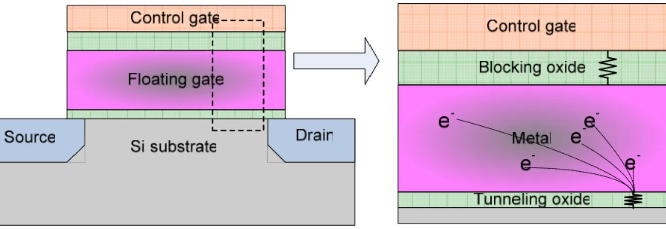
(15) Chapter 1 Introduction 1-1 Evolution of Flash Memory Recently, portable electronic products such as personal digital assistant (PDA), notebook computer, digital camera, intelligent IC card, USB Flash personal disc, etc. develop rapidly to provide better life quality. All of these products require memory technologies. Memory technologies can be divided into two categories according to whether the stored data can be reserved or not without power supply. The former is non-volatile memory and the latter is volatile memory. Non-volatile memory can remain the storage data for a long time even if it encounters the break of power supply. As a result, portable electronic products can reach low power consumption by employing non-volatile memory. 1.1.1 Floating Gate Non-volatile Memory D. Kahng and S. M Sze invented the first floating gate (FG) non-volatile memory at Bell Labs in 1967 [1]. The basic concept of FG non-volatile memory is shown in Fig. 1.1. The FG non-volatile memory has the advantages of large memory window, good program/erase (P/E) speed, and good reliability for commercial applications. Various kinds of FG non-volatile memory have been developed and are applied in our daily life.. 1.
(16) Although a huge commercial success, there are some critical limitations for FG non-volatile memory when scaling down [2-3]. High operation voltages are needed because of the low gate coupling rate. The high voltage operation limits the embedding potential with standard CMOS. When the tunneling oxide thickness scales down, the retention characteristic of FG memory degrades because charges stored in the FG will leak through any defect point in the tunneling oxide which may be generated during P/E operations. At the same time, the endurance characteristic of FG memory is also degraded. It is hard to improve the P/E speed of FG memory because of the non-scalable tunneling oxide thickness. Coupling between floating gates is another issue. It limits the cell density. Therefore, the International Technology Roadmap for Semiconductors (ITRS) predicted that the conventional FG memory can not be scaled down to sub-40 nm node and the other solutions such as MNOS (Metal / Nitride / Oxide / Silicon), SONOS (Silicon / Nitride / Oxide / Silicon) and nano-crystal non-volatile memories with discrete charge storage nodes are suggested [4]. 1.1.2 SONOS Non-volatile Memory The SONOS type non-volatile memory which stores charges in discrete traps of the silicon nitride layer exhibits better retention characteristics so that the tunneling oxide thickness can be reduced to improve the P/E speed and operation voltage [3-5]. The basic concept of SONOS non-volatile memory is shown in Fig. 1.2. Comparing with SONOS memories, the charges stored in MNOS memories may leak from the nitride layer to control. 2.
(17) gate directly [6]. By inserting a top blocking oxide between the control gate and the nitride layer, the leakage current through the control gate is reduced and the retention characteristic is improved. Comparing with FG memories, SONOS memories exhibit many advantages, e.g., higher scaling feasibility, better process compatibility, lower program voltages, and lower power consumption. Unfortunately, there are still many issues for SONOS-type memories such as erase saturation [7]. The operation voltages and power consumption are still not low enough. The movement of stored charges between trapping nodes, which is called “charge migration” [8], is also an issue of SONOS-type memories. The disturbance effects are the result of the share of word-lines and bit-lines in memory array. When we operate one memory cell, unwanted biases may apply on the other cells which share the same word-line or bit-line. The unwanted biases may cause stored charge movement and change the stored data. These concerns must be solved before the mass-production of SONOS-type memories. Some advanced SONOS-type memories such as bandgap engineered SONOS (BE-SONOS) [9-10] or TaN/AlO/SiN/Oxide/Si (TANOS) [11], attracted much more attention for being the next-generation non-volatile memories recently. For the BE-SONOS, the band-gap engineering is implemented by replace the tunneling oxide with an Oxide/Nitride/Oxide (ONO) stack. During program or erase operations, the band offset caused by high electric field reduces the ONO barrier and allows charge tunneling more easily. At low electric field such as during retention, the band offset does not exist and the stored. 3.
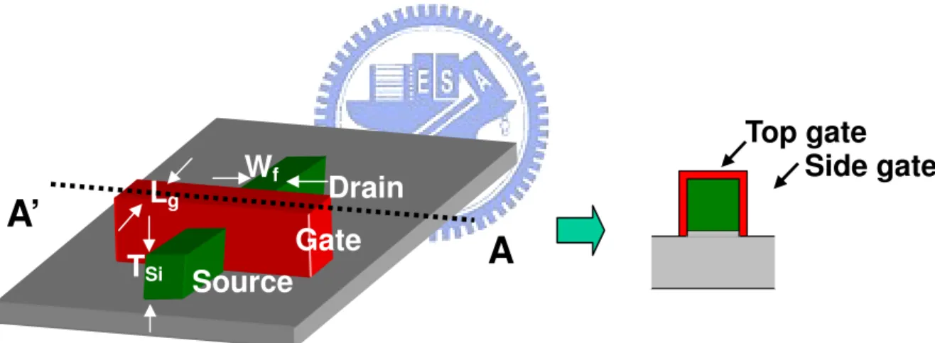
(18) charges are blocked by the entire ONO barrier. As a result, BE-SONOS memory can reach both high P/E speed and good data retention [9-10]. For TANOS memory, because the TANOS memory employs high-k martial as the blocking dielectric, lower operation voltages can be achieved due to good gate coupling to the conductive channel. However, charge migration is still an issue to be solved even for BE-SONOS or TANOS. In order to minimize the charge migration, nano-crystal non-volatile memories have been proposed. 1.1.3 Nano-crystal Non-volatile Memory Nano-crystal non-volatile memories are potential solutions for next generation non-volatile memories. Fig.1.3 shows the basic concept of nano-crystal memories. Nano-crystal memories may have better retention characteristics than SONOS-type memories because nano-crystals effectively prevent from the formation of good conductive paths between traps. Once a defect is generated in tunneling oxide during operation, only the nano-crystal which is the nearest to the defect will be discharged so that good endurance and retention characteristics can be achieved. Therefore, thinner tunneling oxide can be used to reduce the operation voltages and to improve the P/E speed without degrading the retention characteristic. The disturbance characteristics can be improved because the charge migration is suppressed when the energy barrier between nano-crystals and the surrounding dielectric is high enough. The nano-crystal memories can implement 2-bit operation or multi-level operation [12], which can increase the memory density. Because of higher density of states for charge trapping and stronger gate coupling, the improvement of retention characteristics can be achieved by using metal nano-crystals such as Au, Ag, Pt and TiN etc. [13-16]. The freedom of engineering of the work function of nano-crystals for optimizing the device characteristics is additional advantage. 4.
(19) Nano-crystals can be fabricated by several techniques including chemical vapor deposition [16], annealing of or ultra-thin metal layer [17] or silicon rich oxide layer [18], low energy ion implantation [19], thermal oxidation SiGe layer [20-21], and aerosol nano-crystal formation [22]. In order to achieve superior memory characteristics, the size of nano-crystal should be optimized, the high density of nano-crystal is needed, and the distributions of nano-crystal should be uniform [23]. Recently, nano-crystal non-volatile memory with multi-gate structure has demonstrated a memory window of 8V and only 17% charge loss after 5×10⁴ seconds. The program speed for maximum window is about 10 µsec [24]. 1.1.4 Multi-gate Memory It has been reported that multi-gate structure can be used to improve the performance of memory cell [28]. Multi-gate MOSFET has been predicted as a candidate for memory beyond 45 nm node [1]. Fig.1.4 shows the schematic of multi-gate structure. Recently, various SONOS-type and nano-crystal memories have been fabricated with multi-gate structure [25-29]. It has been reported that employing this structure can get better short channel controllability, higher driving current, lower leakage current, better programming inhibition, and more numbers of nano-crystals [27-32]. Furthermore, because of the charge storage at the two opposite sidewall channels, the body potential is favorably modulated. As a result, larger memory window, longer retention time, and higher endurance can also be achieved [28].. 1-2 Motivation We have mentioned that metal nano-crystals, such as Au, Ag, Pt and TiN, have been reported in aiming to improve memory characteristics. Faster P/E speed can be achieved because of the stronger coupling with the conduction channel by using nano-crystal. Metal materials have higher density of states around Fermi level. They can provide more charge traps. The non-volatile memory with metallic nano-crystal has larger memory window and 5.
(20) better retention characteristics. The work function of TiN is extracted to be about 4.6eV [30, 33], it is expected to provide about 0.6eV deeper traps than that of silicon nano-crystals. So, nano-crystal non-volatile memory with TiN nano-crystal really should exhibit better performance than nano-crystal non-volatile memory that with semi-conductor nano-crystal. In this work, TiN nano-crystals will be fabricated by annealing TiN/Al2O3 nano-laminates. We have also mentioned that the non-volatile nano-crystal memory can be operated at lower operation voltage by employing the metal nano-crystal such as TiN nano-crystal. This is because of the enhancement of the gate coupling with conduction channel by using metal nano-crystal to reduce the total dielectric thickness. Gate coupling can also be enhanced and the operation voltage can be suppressed by using high-κ dielectric material. Therefore, High-κ dielectric material, Al2O3, is used for blocking oxide in this work. The influences of blocking oxide thicknesses on memory characteristics will be studied. In this work, multi-gate structure is use to provide better transistor performance as well as memory characteristics. The better gate control ability and larger active channel width of the multi-gate structure improve on-current characteristic with respect to conventional planar devices. In addition, SOI wafers are used to suppress punch through and the effective gate control ability becomes better. Due to the better gate control ability and the suppression of punch through, multi-gate cell transistors also show better subthreshold swing and lower off-current characteristic. It can provide memory cells better retention characteristic and low power operation. The TiN nano-crystal non-volatile memory with planar structure has been proposed [30] and good memory performance could be obtained. The device geometry in [30] is larger than the state-of-the-art. In this work, nano-scale TiN nano-crystal non-volatile memory with multi-gate structure will be fabricated to evaluate the scalability of the TiN nano-crystal memory cell.. 6.
(21) Moreover, it was reported that nano-crystal size affects memory characteristics deeply and the annealing time and film thickness affects the formation of nano-crystal. The nano-crystal formation conditions, film thickness, and annealing time should be optimized to achieve superior memory characteristics. We will discuss the effects of the post-deposition annealing time and film thickness for TiN nano-crystal formation on memory characteristics. In addition, we used p+ poly gate to improve the erase characteristics by suppressing the electron back tunneling (EBT) from control gate during erase [32] because its high work function can suppress the electron injection through blocking oxide during erase operation. After process tuning, non-volatile memory with superior memory characteristics such as large window, excellent endurance, and long retention time can be expected.. 1-3 Thesis Organization This thesis is divided into four chapters and the contents of each chapter are described as follows. In chapter 2, the fabrication process of 80nm gate length multi-gate TiN nano-crystal non-volatile memory on SOI wafer will be described. We also list different process conditions such as the thickness of TiN layer, anneal times… etc. The electrical measurement conditions are also mentioned in chapter 2. In chapter 3, the basic transistor characteristics of the TiN nano-crystal non-volatile memory fabricated in chapter 2 will be discussed firstly. We will show that the TiN nano-crystal flash memory using thicker TiN nano-laminate has larger memory window of about 5V and good retention of 8% charge loss after 104 sec, and high endurance of 7% degradation after 104 P/E cycles. We also link the better retention characteristics with smaller gate leakage current and vise versa. In addition, we also present a novel memory operation scheme by sensing the level of off-region current after ban-to-band hot hole programming. 7.
(22) Negligible memory window narrowing after 106 seconds and low voltage operation have been demonstrated. Finally, conclusions and future works are presented in chapter 4.. 8.
(23) Fig. 1.1: The basic concept of floating gate (FG) non-volatile memory.. Fig. 1.2: The basic concept of SONOS non-volatile memory.. 9.
(24) Fig. 1.3: The basic concept of nano-crystal non-volatile memory.. A’. Lg TSi. Wf. Top gate Side gate. Drain Gate. A. Source. Fig. 1.4: The schematic of multi-gate structure.. 10.
(25) Chapter 2 Experimental Procedure 2-1 Introduction In this chapter, a novel technique to form localized TiN nano-crystals which is fully compatible with CMOS technologies is presented. As mentioned in previous chapter, the work function of TiN is about 4.6eV, and it is expected to provide about 0.6eV deeper traps than that of Si nano-crystals [33]. Therefore, memory cells using TiN nano-crystals is expected to exhibit superior memory characteristics, such as long retention time and strong immunity against disturbance. The TiN nano-crystals are formed by a cyclic deposition of TiN/Al2O3 layers followed by rapid thermal annealing. These TiN nano-crystals are readily isolated from each other within an Al2O3 matrix. The memory characteristics with different TiN deposition thicknesses and annealing times will be examined. Besides, combining with multi-gate structure on SOI wafer, leakage current could be suppressed and low power operation can be achieved when scaling [27-32]. Also, the retention characteristics and memory window can be improved [28]. The detailed process flow for device fabrication and the process conditions will be described in the next section.. 11.
(26) 2-2 Device Fabrication Fig. 2.1 shows the main process flow of the n-channel multi-gate TiN nano-crystal non-volatile memory. The devices were fabricated on a 6” SIMOX SOI wafer with a lightly boron doped SOI layer as shown in Fig.2.1(a). The doping concentration of the SOI layer is around 1x15 cm-3. The thicknesses of the SOI layer and the buried oxide layer are 40nm and 150nm, respectively. Fin-type active area in (110) orientation with fin width of 50 nm were patterned by e-beam lithography with negative e-beam (NEB) resistance and plasma etching at first. The tunneling oxide was thermally grown to 4 nm thick in a vertical furnace system at 800°C in dilute oxygen gas ambient. Then, TiN (0.5nm or 0.7nm)/Al2O3 (1.0nm) nano-laminate with 7 periods were deposited in a PEALD/ALD system and a 15 nm or 20 nm thick Al2O3 was deposited as blocking dielectric in the same ALD system followed by a deposition of 150 nm thick LPCVD poly-Si gate at 550°C. TiN was deposited with TiCl4 as precursor at 350°C and Al2O3 was deposited with Al(CH3)3 as precursor at 300°C. Post deposition annealing (PDA) was performed at 900°C for 10 sec and 40 sec in nitrogen gas ambient to form TiN nano-crystals. Then, the poly-Si gate was heavily doped to p-type by BF2+ ion implantation at 40KeV to a dose of 5x1015cm-2. Gate dopant activation was performed by RTA annealing at 900℃ for 20 seconds in nitrogen gas ambient. Before gate patterning, TEOS oxide with a thickness of 80nm was deposited on the poly-Si film as an hard mask to avoid unexpected anti-doping during n+ S/D ion implantation (Fig. 2.1(b)).. 12.
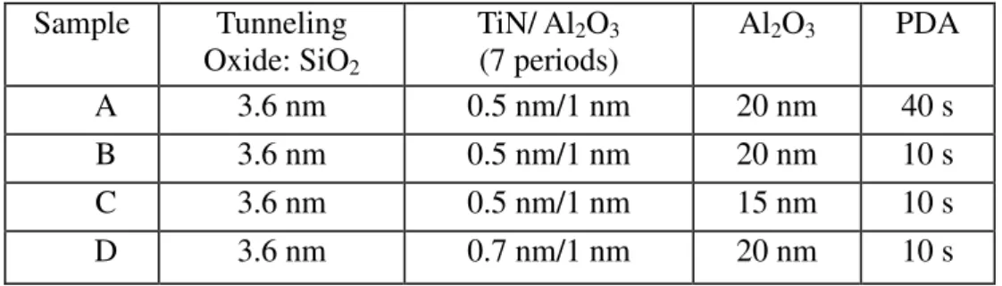
(27) During gate patterning, the gate patterns were transfer from e-beam photo resist to hard mask by plasma etching at first. And then, the TEOS oxide acted as hard mask to finish the remaining etching steps. The cross-sectional structure after gate patterning is shown in Fig. 2.1(c). Next, a SiO2/Si3N4 composite spacer with thickness equals to 10 nm and 40 nm was formed as shown in Fig. 2.1(d). Then, P31+ ions were implanted into S/D region at 20 KeV to a dose of 5x1015 cm-2 and were activated at 900 °C for 20 sec in nitrogen gas ambient as shown in Fig. 2.1(e). Native oxide on S/D region and the gate hard mask were removed by dipping in dilute HF solution to form the structure shown in Fig.2.1(f). Ni film was deposited in a sputtering system to a thickness of 25nm followed by a two-step Ni-salicide process [35]. After first step annealing at 300℃ for 45 min in vacuum to form Ni2Si phase, unreacted Ni was removed by H2SO4/H2O2 = 3:1 solution and the second step annealing was performed at 600℃ for 30 seconds to transform Ni2Si phase to NiSi phase. The H2SO4/H2O2 = 3:1 solution was used again to make sure the unreacted Ni was removed completely. The S/D region was converted to fully silicide structure and the gate electrode became Ni-polycide structure as shown in Fig. 2.1(g). Table 2.1 summarizes the split conditions used in this thesis. The listed post deposited annealing time (PDA) is the RTA time of the post-Al2O3/TiN laminates deposition annealing, not including the gate dopant activation annealing (20 sec) and S/D dopant activation annealing (20 sec).. 13.
(28) 2-3 Electrical Characterization Techniques To characterize the multi-gate TiN nano-crystal non-volatile flash memory fabricated in this thesis, the following measurements were performed. Static current-voltage (I-V) characteristics of the memory cell were measured using a semiconductor parameter analyzer of model Agilent 4156C. During program and erase operations, an Agilent 41501A pulse generation expander was used to generate pulse signals. The threshold voltage (Vt) is defined as the applied gate voltage at which the drain current is 0.1 µA as the drain voltage is 1V. The gate voltage sweeping range during I-V measurement should be controlled and adjusted in time carefully; otherwise, unexpected Vt shift may occur. If necessary, the I-V curve was recorded repeatedly to make sure that the gate bias did not make Vt shift. The definition of memory characteristics and methods to measure these characteristics are described as below: (A) P/E speed and memory window To characterize the P/E speed, Vt was measured after each program or erase operation at different P/E conditions such as different gate biases and different pulse widths. During program and erase operations, both source and drain terminals were biased at 0V because FN tunneling is used for charge injection in this work. When measuring P/E speed, the Vt or Vt shift were recorded at different pulse widths. The “Vt shift” is defined as the change of Vt after each program or erase operation. It should be noted that the device must be restored to the initial. 14.
(29) state, i.e. the state before the first program or erase operation, before applying another P/E signal. Otherwise the P/E performance will be overestimated. The memory window is defined as the Vt difference between program state and erase state. (B)Retention Retention characteristics are defined as the change of program state and erase state as time goes by at different storage temperatures. The Vt, Vt shift, charge loss or charge loss rate could be used as the indicator of retention performance. Charge loss or charge loss rate can be extracted from the changes of memory window with storage time. Besides, to avoid unexpected program or erase, small Vg sweeping range should be used to monitor Vt during storage. The ten year residual memory window can be extrapolated from the Vt-time correlation. (C)Endurance Endurance is defined as the Vt for both program state and erase state during sequential P/E cycles. More than 104 times P/E cycles were measured in this thesis. A sequential pulse signals at fixed pulse width and rise/fall time were pulsed into memory cells. It is not necessary to reach the maximum memory window to evaluate endurance or the device may break too easily during measurement. (D)Disturbance. 15.
(30) There are three kinds of disturbances for flash memories, read disturbance, gate disturbance, and drain disturbance. The disturbance effects are due to the share of the word line and the bit line in a memory array. The read disturbance is defined as the change of the stored data, Vt, during read operation. Gate disturbance is defined as the change of Vt by the un-wanted gate voltage during program or erase operation. Drain disturbance is defined as the change of Vt by the un-wanted drain voltage during program or erase operation. Which disturbance should be characterized depends on what kind of memory array and what mechanisms are used for P/E operations. For NAND array, only the FN tunneling is used for both program and erase operations. Therefore, only read disturbance and gate disturbance were presented because the multi-gate TiN nano-crystal non-volatile flash memory was designed as the NAND array flash memory. The source and drain terminals were floating when measuring the gate disturbance and the drain disturbance issue is not existent. When measuring, memory cell were stressed and the I-V characteristic was measured at specific times.. 16.
(31) Table 2.1: Process conditions of the multi-gate TiN nano-crystal nonvolatile memory fabricated in this thesis. Sample Tunneling TiN/ Al2O3 Al2O3 PDA Oxide: SiO2 (7 periods) A 3.6 nm 0.5 nm/1 nm 20 nm 40 s B 3.6 nm 0.5 nm/1 nm 20 nm 10 s C 3.6 nm 0.5 nm/1 nm 15 nm 10 s D 3.6 nm 0.7 nm/1 nm 20 nm 10 s. 17.
(32) SOI BOX. Si Sub.. (a). Gate Hardmask. Poly-Si Gate Al2O3 SOI BOX. Si Sub.. (b). 18.
(33) Gate Hardmask PolySi Gate Al2O3 SOI BOX. Si Sub.. (c). Gate Hardmask PolySi Gate Al2O3 SOI BOX. Si Sub.. (d) 19.
(34) Gate Hardmask PolySi Gate Al2O3 N+. SOI. N+. BOX. Si Sub.. (e). PolySi Gate Al2O3 N+. SOI BOX. Si Sub.. (f) 20. N+.
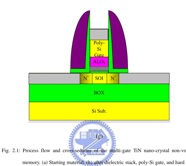
(35) PolySi Gate Al2O3 N+. SOI. N+. N+. BOX. Si Sub.. (g) Fig. 2.1: Process flow and cross-sections of the multi-gate TiN nano-crystal non-volatile memory. (a) Starting material, (b) after dielectric stack, poly-Si gate, and hard mask deposition, (c) after gate patterning, (d) after spacer formation, (e) after S/D ion implantation, (f) after S/D activation and gate hard mask removal, (g) after silicide formation.. 21.
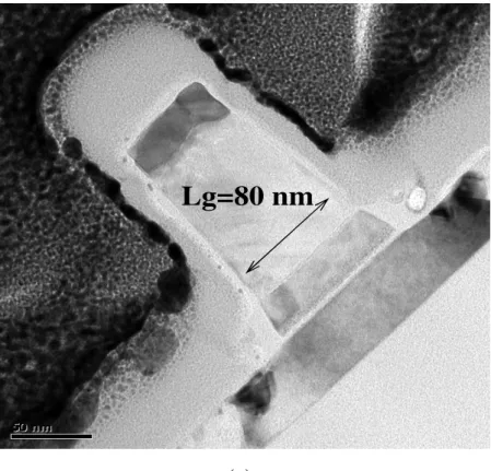
(36) Chapter 3 Characteristics of TiN Nano-crystal Non-volatile Memory 3-1 Introduction In this chapter, we discuss the memory characteristics of the TiN nano-crystal memory devices. Basic memory characteristics including memory window, P/E speed, retention, endurance, and disturbance of the memory cells are evaluated carefully and the effect of different process conditions such as the thickness of ALD-deposited TiN layer, the annealing temperature for nano-crystal formation, and the thickness of blocking oxide are also examined. In addition, we presented a novel memory operation scheme. This novel memory operation scheme is done by sensing the level of off-region current. The level of the off-region current could be controlled. It changes after some operations and maintains for a long time. This novel phenomenon will be presented and the possible mechanism will be discussed briefly.. 3-2 Device Structure Inspection Transmission electron microscopy (TEM) images of the multi-gate TiN nano-crystal non-volatile memory (sample A) with gate length of 80nm and fin width of 50nm are shown. 22.
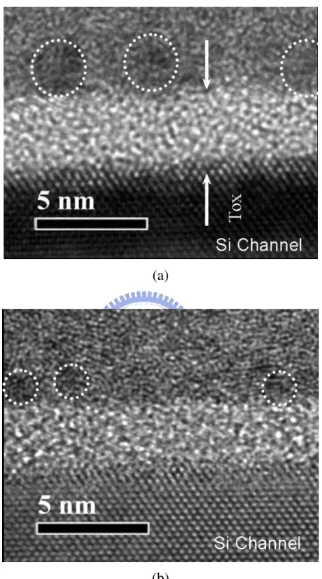
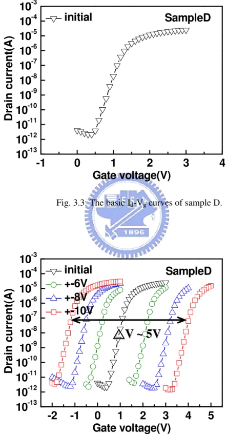
(37) in Fig. 3.1(a) and Fig. 3.1(b). It can be found that the Al2O3 blocking layer is crystallized. This may affect the retention performance and will be discussed later. The high-resolution TEM image of TiN nano-crystals of sample D and sample A are shown in Fig. 3.2(a) and (b) respectively. The tunneling oxide thickness is about 3.6nm. It can be found that TiN nano-crystals in sample D have average diameter about 2nm and sample D has larger TiN nano-crystals than sample A. That may because of thicker TiN layers in sample D and there are more sufficient material for formation larger TiN nano-crystals. The size of nano-crystal influences memory performance and we will discuss it later. Moreover, Fig. 3.2 also shows that the TiN nano-crystals are embedded in Al2O3. The discretion of the nano-crystals prevents from the formation of effective conduction paths that are accounted for the degradation of retention characteristics.. 3-3 Basic Electrical Characteristics All cells discussed in this chapter have dimensions of L/W = 80nm/50nm. The basic Id-Vg curve of sample D is shown in Fig. 3.3. Usually, higher current (better driving capability), lower off current, and smaller subthreshold swing are preferred for a transistor. In Fig. 3.3, it is found that there is a superior driving capability of 268uA/um at |VDS|=|VG-Vt|=1V because the good gate control ability of multi-gate structure [28, 39]. Besides, the measured subthreshold swing is about 110 mV/dec and the EOT of gate stack is. 23.
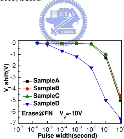
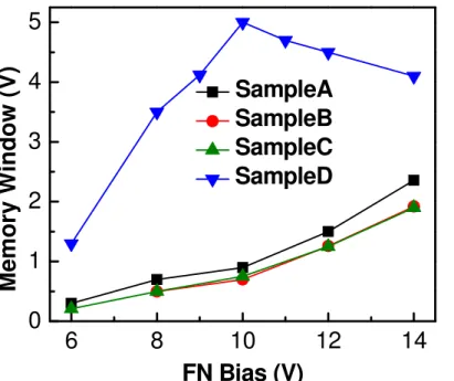
(38) about 15nm.. 3-4 P/E Speed and Memory Window Fig. 3.4 shows the Id-Vg curves of sample D with programming time of 0.1 sec at different P/E voltages. FN tunneling is used for both program and erase operation. It can be found that there is a large memory window about 5V between the write and erase states after P/E operations at ±10V. Because of the large memory window, multi-level operation can be realized by choosing P/E operation biases carefully. The Vt shift after program and erase at Vg = ±10V for different pulse widths and different gate stack conditions are shown in Fig. 3.5 and Fig. 3.6, respectively. It is observed that the program and erase speed increase dramatically when the TiN layer thickness increases from 0.5nm (sample A-C) to 0.7nm (sample D) because thicker TiN layer has more sufficient material to form larger TiN nano-crystals as shown in Fig. 3.2. On the other hand, the memory window is slightly increased by extending the PDA time from 10 sec (sample B) to 40 sec (sample A). It is suspected that longer annealing time helps the formation of TiN nano-crystals. Furthermore, the device with thinner blocking oxide of 15nm (sample C) has almost the same memory window as compared with the device with thicker blocking oxide of 20nm (sample B). This result indicates that the electron back tunneling (EBT) through the blocking oxide is negligible at Vg = ±10V.. 24.
(39) Fig. 3.7 shows the memory windows of samples A-D after programming at different gate voltages for 0.1 sec. Sample A has slightly larger memory window than samples B and C because sample A experienced longer PDA time. However, sample D, with thicker TiN layer thickness, exhibits much larger memory window. The memory window of sample D increases with the increase of biases up to ±10V and then decreases with the further increase of the biases. The maximum window is about 5V and is obtained at ±10V. For 1 sec P/E pulse width, the higher P/E voltage results in the smaller Vt shift at either program or erase operation. The turn-down of memory window at high P/E voltage is usually explained by the EBT effect. However, if EBT occurs at Vg higher than ±10V, the memory window of the other samples should be also turned-down because those samples have similar or thinner blocking oxide layer. This is not observed in Fig.3.7. Therefore, we propose a new turn-down model. Because sample D has larger TiN nano-crystals, more charges can be stored in the nano-crystals during programming. Therefore, the electric field between the charged nano-crystals and gate, i.e. in the blocking oxide, would be much higher than that of the other samples. Some charges may escape by tunneling through the blocking dielectric to gate electrode so that the Vt shift is turned-down. Similar effect occurs during erasing. This explanation is very possible because the blocking oxide is crystallized as shown in Fig. 3.1. Program characteristics of sample D as a function of pulse widths and gate biases are shown in Fig. 3.8. Meanwhile, the erase characteristics of sample D with different erase. 25.
(40) conditions are displayed in Fig. 3.9. The Vt shift increases with the increase of P/E pulse width and P/E voltage as the pulse width is shorter than 0.1 sec. As the pulse width increase to 1 sec, the higher the P/E voltage is, the smaller the Vt shift is. This phenomenon indicates that as the charges stored in nano-crystals increases to certain extend, turn-down of Vt shift will occurs no matter what the charges are injected into nano-crystals by high P/E voltage or long P/E pulse width. Since the EBT mechanism depends on the P/E voltage only but not on the pulse width, the observation in Fig.3.8 and Fig.3.9 confirms the model proposed to explain the turn-down phenomenon shown in Fig.3.6 and Fig.3.7. The program speed shown in Fig.3.5 to Fig. 3.9 is slow in compared with literature even for sample D, which has the fastest program speed among samples A-D. This low program speed may attribute to the tiny TiN nano-crystals. It has been mentioned in section 3-1 that the average size of TiN nano-crystals in this work is about 1~2nm. It is much smaller than the optimum nano-crystal size, 5nm [23]. The small nano-crystals will decrease the trapping efficiency during program operation due to coulomb blockade and quantum confinement effects [23, 40]. To increase the program speed and the memory window, the size of TiN nano-crystals must be increased. Possible methods will be discussed in future works.. 3-5 Retention 3.5.1 Retention performance with different P/E states. 26.
(41) To study the effect of P/E level on the retention performance, Vt of sample C was monitored after P/E to the same memory window but different Vt levels: the strong program state and the strong erase state. For the strong program state, the program voltage is higher than the erase voltage. For the strong erase state, the erase voltage is higher than the program voltage. The results are shown in Fig. 3.10. After 103 seconds, the strong erase state exhibits a charge loss of about 38 % while the strong program state only loss 20% charges. This difference can be explained by the band diagram shown in Fig. 3.11. After higher erase bias, more holes will be injected into the nano-crystals and induces higher electric field between nano-crystals and Si body. In this case, holes have higher probability to tunnel to Si body. To obtain better retention characteristic, the position of the memory window must be selected carefully. 3.5.2 Correlation between retention characteristic and gate leakage current There is undesirable poor uniformity of retention characteristics even in the same process conditions and the same cell size in these multi-gate TiN nano-crystal non-volatile memories. Some memory cells exhibit obvious poorer retention characteristics than the others. These cells exhibit the same subthreshold swing and memory window with the others but poorer retention characteristics. It is also found that some cells have obvious higher gate leakage but the others do not. Therefore, the relationship between gate leakage current and retention characteristics is examined.. 27.
(42) Fig. 3.12(a) shows the remnant charge in percentage of difference cells with the same cell size in sample C after storage at 25℃ for 600 sec. Because the retention degradation rate is affected by the P/E state, all of the cells were tuned to the same program state of 2V, which means 1V window between initial state (1V). The corresponding Ig-Vg curves of these cells at fresh state are shown in Fig. 3.12(b). It can be found that the cells with higher gate leakage current tend to have poorer retention characteristics and vice versa. It can be directly perceived through the senses that the cells have higher gate leakage current loss the stored charge quickly. The larger gate leakage current may because of the corner effect of Si fin or the crystallization of Al2O3. As for the corner effect of Si fin, the corner enhanced electric field near the fin corner will increase the discharge probability of trapping nodes which are near the fin corner. The larger gate leakage current may also result from the blocking Al2O3 crystallization, as shown in Fig.3.1, which increases the leakage current path. The Al2O3 grain is about few ten nanometers. Such large crystals may increase the stress in gate stack which is also claimed for forming defects to be good leakage paths. 3.5.3 Average retention characteristics of sample A-D Fig. 3.13 compares the remnant charge in percentage of sample A-D with the same cell size after storage at 25℃ for 600 sec. It has been mentioned before that because the remnant charge is affected by the program/erase state selected, all of the cells are tuned to the same program state to 2V that means 1V memory window between initial state (1V). It can be. 28.
(43) found that although sample D (with memory window about 5V) has larger memory window than the others such as sample B (with memory window about 1V) and sample C (with window about 1V), the remnant charge distributions of the four samples are similar. That is, even sample D has much larger memory window than the others; it does not have outstanding retention performance if we tuned the program state to 2V. The distributions of gate leakage current of sample A-D at Vg = ±16V are shown in Fig. 3.14. Obviously, the gate leakage current of sample D (TiN layer thickness is 0.7nm, PDA = 10 sec. blocking oxide = 20nm) is higher than the others even if it has thicker blocking oxide than sample C (TiN layer thickness is 0.5nm, PDA = 10 sec. blocking oxide = 15nm). It has been shown in Fig.3.12 that the devices with higher gate leakage current tend to have poorer retention performance. Therefore, because of the gate larger leakage current, sample D do not has outstanding retention performance than the others even it has much larger memory window. The high gate leakage current of sample D may due to the thick TiN layer. The larger nano-crystals may exert higher stress on the tunneling oxide and/or the blocking dielectric. The only process difference between sample B and sample C is the thickness of Al2O3 blocking layer – 20 nm for sample B and 15nm from sample C. Although the average gate leakage current of sample C is slightly higher than that of sample B, the difference is much smaller than the process variation. It is reasonable to say that the gate leakage current is not determined by the Al2O3 blocking layer. Therefore, the high gate leakage current of sample D. 29.
(44) should be attributed to the large nano-crystals induced leakage current of the tunneling oxide. 3.5.4 Retention performances of sample A-D The retention characteristics of the TiN nano-crystal memory devices of sample A (TiN layer thickness is 0.5nm, PDA = 40 sec) and sample D (TiN layer thickness is 0.7nm, PDA = 10 sec) at 25℃ and 85℃ are shown in Fig. 3.15. The devices shown in Fig. 3.15 are selected for the best retention performance. In order to compare the retention degradation rate with sample A, the memory window of sample D was tuned to identical to that of sample A. For sample D, only 6% charges are lost at 25℃ after 104 sec. Extrapolating to 10 years, more than 88% charges are reserved. The charge loss is more serious at 85℃ than at 25℃ for both sample A and sample D. In addition, the charge loss is more serious for sample A (with memory window of about ~1.4V) than sample D (with memory window of about ~5V) if both samples are P/E to the same memory window at the beginning of retention time. Sample D has larger memory window than sample A. This difference indicates that sample D can store more charges than sample A because sample D has larger nano-crystal size. At the same memory window, charges stored in nano-crystals have not reach saturation so that the charges encounter less Coulomb repulsive force. On the other hand, there exists stronger Coulomb repulsive force between stored charges in sample A. The stronger Coulomb repulsive force will discharge the stored charges from trapping nodes more quickly and increase the charge loss rate [23, 40]. Furthermore, strong quantum confinement of sample A may increase the. 30.
(45) trap energy so that the stored charges can escape from traps easily.. 3-6 Endurance performance During P/E cycles, the electron trapping phenomenon, such as hard-to-erase may happens because of the spatial distributions for electrons and holes in nano-crystal non-volatile memory are localized [9, 36, 43]. If the electron distribution does not completely match that for hole after every program or erase operation, then every P/E cycle leaves a few electrons in trapping layer resulting in a slight increasing in Vt. Therefore, memory window decreases after numerous P/E cycles. However, this is not an issue for our memory because FN tunneling is used for both program and erase operation [9, 43]. Therefore, not only electrons but also holes have uniform distribution in trapping layer and the distribution mismatch is negligible and good endurance performance can be obtained. The endurance performance of sample D is shown in Fig. 3.16. The memory window shows only 7% degradation for sample D and only 3% degradation for sample A even after 104 P/E cycles. The degradation of the I-V characteristic of sample D is also examined in Fig. 3.17, which is correlated to the deterioration of the tunneling oxide quality during 104 P/E cycles. Invisible shift of the program and erase states means that the incomplete electron de-trapping during 104 P/E cycles is negligible in this TiN nano-crystal non-volatile memory [36]. In addition, the slightly degradation of subthreshold swing after 104 P/E cycles indicates that the tunneling. 31.
(46) is not deteriorated severely during program and erase. This endurance performance is much superior to that of the published planar nano-crystal memories and could be understand by the electric field cancellation in multi-gate devices [45].. 3-7 Disturbance performance There are three kinds of disturbances: read disturbance, gate disturbance, and drain disturbance. The disturbance effects are due to the share of the word line and the bit line in a memory array. And the arrangements of word line and bit line are different in NOR array and NAND array. Therefore, which disturbance characteristics should be considered depends on which memory array is adopted. Fig. 3.18 and Fig. 3.19 show the two memory arrays, NOR array and NAND array, respectively. For NAND array, the elementary unit is not composed of the single three-terminal cell such as shown in Fig. 3.19(a), which stores one bit, but by more memory cells connected in a series. It constitutes a chain connected to the bit line and grounded through two selection transistors. The structure allows the elimination of all contacts between word lines. Thus, NAND array reducing the occupied area by about 40% and high memory density can be achieved [37, 41, 42]. Cells in NAND array are operated by FN tunneling in general. Since our multi-gate TiN non-volatile memory is targeted for NAND application and is operated by FN tunneling, read and gate disturbance characteristics are examined and drain disturbance is not an issue. From the previous discussions, sample D. 32.
(47) exhibits the best performance among the four samples. Therefore, the disturbance performance of sample D is examined here. Fig. 3.20 shows the read disturbance characteristics of sample D at the erase state. The word-line voltage during read operation may result in electron injection or hole-detrapping and induce unwanted Vt shift in the cells sharing the same word line. On the other hand, bit-line voltage during read operation may cause unwanted channel hot electrons injection and result in a Vt shift [38, 44], too. Fig.3.20 reveals that the read disturbance after 1000 sec in this multi-gate TiN nano-crystal non-volatile memory is very weak. The negligible read disturbance is attributed to the really localized nano-crystals. Hence, the stored charges can only migrate slightly under the low read bias. Fig. 3.21 and Fig. 3.22 show the gate disturbance characteristics at erase state and program state, respectively. Gate disturbance may happen during program or erase operation on the cells sharing the same word line while one of them is being programmed or erased [44]. Therefore, word-line voltage may stress the cells and cause unwanted migration of stored charges. The gate disturbance at erase state was measured with the condition at Vg = ±10V and Vs = Vd = floating for 1000 sec. It is observed that there are negligible disturbances after 1000 sec stress. This excellent gate disturbance performance is attributed to the floating body of multi-gate structure on SOI wafer. During stress, the source and drain terminals as well as the body potential are floating. The electric field drop on the trapping layer is reduced to. 33.
(48) reduce the unwanted tunneling current and unwanted charge migration. Fig.3.22 shows that the erase voltage (-10V) may disturb the program state than the program voltage (+10V). It is known that only few charges are stored in the nano-crystals at erase state while lots of electrons are stored at program state. During program stress, it is hard to inject more electrons into the nano-crystals because of the coulomb repulsion and the floating body. However, some stored electrons may be detrapped by the high negative erase voltage during erase stress so that negative Vt shift can be observed. It should be noted that this disturbance is saturate at several tens seconds and should not be a serious issue.. 3-8 Control the off-region current During the measurements presented previously, it is found that the off-region current of the TiN nano-crystal multi-gate memory cell can be switched between two different levels. At first glance, this phenomenon looks like the gate induced drain leakage (GIDL) current which has been proposed in literature [46-47]. Fig. 3.23(a) and Fig. 3.23(b) show the Id-Vg characteristics of forward read and reverse read that changes after channel hot electron (CHE) and band-to-band hot hole (BBHH) stress for 0.1~0.2 sec, respectively. The stress conditions are listed in Table 3.1. It is found that the off-region current saturates quickly at the level of about 1x10⁻¹⁰ A under either forward read or reverse read before CHE or BBHH stresses. This state is called “initial state” or “erase. 34.
(49) state” in the following part of the thesis. It is interesting that CHE stress also does not change the off-region current. This is the first difference from the published GIDL phenomenon. In those literature, the off-region current increases after CHE stress. The reverse-read off-region current is suppressed to the level of about 1x10-12A after BBHH stress. It is called the “program state”. The forward-read off-region current does not change. This is the second difference from the GIDL phenomenon. In those literatures, the GIDL is more pronounce under forward read but not reverse read. The program state can be restored by CHE stress. Then, the off-region current rises to the original value of about 1x10⁻¹⁰A, erase state. By sensing the forward-read and reverse-read current at program state or erase state, a novel memory operation scheme can be realized. About two orders of magnitude resistance change can be obtained and it is sufficient for data storage. Retention performance at 25℃ and 85℃ are shown in Fig. 3.24. Outstanding retention performance can be obtained. The degradation of memory window is negligible even after 106 and 105 seconds at T=25℃ and T=85℃, respectively. In order to understand the data storage mechanism, we focus on the cause of the off-region current. The Id-Vg curves with different temperature are shown in Fig 3.25(a). Fig 3.25(b) magnifies a part of the off-region current in the Vg range of -2V to -3 V. Obviously, the off-region current is almost independent of the temperature and shows weak gate bias. 35.
(50) dependence. The components of current in off-region at 25℃ are shown in Fig. 3.25(c). It can be found that both source current and drain current flow into gate electrode. The summation of source current and drain current equals to the gate current precisely. This is the third difference from the GIDL phenomenon since GIDL current flows from drain to body or source but not gate. All of the evidences indicate that the observed switching of off-region current can not be explained by GIDL. It seems a resistive-RAM type memory. Leakage path through gate stack may pre-exist in the fresh device. The leakage path may be the percolated oxygen vacancies in the charge trapping layer or blocking layer. CHE stress does not change the leakage path while BBHH may destroy the leakage path by drifting the positive-charged oxygen vacancies so that the off-region current is reduced after BBHH stress. CHE stress may re-allocate the oxygen vacancies to form the leakage path again. Therefore, the off-region current recover to the fresh level. The leakage current level may be limited by the thick blocking layer. This is a very preliminary model for this novel operation scheme. Lots of efforts should be devoted to understand the details. The other memory parameters such as P/E speed, endurance, disturbance, etc. have to be evaluated as well.. 3-9 Summary 36.
(51) The memory performance of the n-channel multi-gate TiN nano-crystal memory device with p+ poly-Si gate and Al2O3 high-k blocking dielectric layer is evaluated in this chapter. Device using thicker TiN layer in the TiN/Al2O3 nano-laminate has larger memory window of about 5V. Therefore, multi-level operation is feasible with different bias conditions. Good retention of 6% charge loss after 104 s and high endurance of 7% window narrowing after 104 P/E cycles are exhibited. The small read and gate disturbance characteristic show the fact that the TiN nano-crystal memory cell is adaptive to the application of NAND type flash memory. Memory performances of sample A-D are summarized in Table 3.2. In addition, we present a novel memory operation scheme by sensing the level of off-region current after band-to-band hot hole programming. Negligible memory window narrowing after 106 seconds and low voltage operation have been demonstrated. The mechanism of this operation scheme and outstanding retention performance is not clear at this moment and it is worthy to be investigated.. 37.
(52) Table 3.1 Bias conditions of BBHH program, CHE erase and read.. Program. Erase. Forward Read Reverse Read. Mechanism. BBHH. CHE. Off-current. Off-current. VG. -6V. 6V. 6~-3V. 6~-3V. VD. 6V. 6V. 1V. 0V. VS. 0V. 0V. 0V. 1V. Table 3.2 Memory performances of various gate stack conditions. Sample. Memory window. Remnant charge. Endurance ( 104 cycles). A. ~1.4V / ±10V, 0.1s ~0.05V / ±10V, 1ms. 0.804% / 600s / Program state = 2V. 97% / 1V. B. ~1V / ±10V, 0.1s ~0.05V / ±10V, 1ms. 0.765% / 600s / Program state = 2V. 99% / 1V. C. ~1V / ±10V, 0.1s ~0.05V / ±10V, 1ms. 0.766% / 600s / Program state = 2V. 100% / 1V. D. ~5V / ±10V, 0.1s ~1V / ±10V, 1ms. 0.847% / 600s / Program state = 2V. 93% / 4V. 38.
(53) Lg=80 nm. (a). Wd = 50nm. (b) Fig. 3.1: The high resolution TEM image of cross-section view (a) of channel length and (b) of channel width.. 39.
(54) (a). (b). Fig. 3.2: The high resolution TEM image of TiN nano-crystals (a) of sample D (b) of sample A.. 40.
(55) Drain current(A). -3. 10 -4 10 -5 10 -6 10 -7 10 -8 10 -9 10 -10 10 -11 10 -12 10 -13 10 -1. initial. 0. SampleD. 1 2 Gate voltage(V). 3. 4. Fig. 3.3: The basic Id-Vg curves of sample D.. Drain current(A). -3. 10 -4 10 -5 10 -6 10 -7 10 -8 10 -9 10 -10 10 -11 10 -12 10 -13 10. initial +-6V +-8V +-10V. SampleD. △V ~ 5 V. -2. -1. 0 1 2 3 Gate voltage(V). 4. 5. Fig. 3.4: The Id-Vg curves of the memory Id-Vg curves of sample D with programming time of 0.1 sec at different P/E voltages.. 41.
(56) 7. Vt shift(V). 6 5 4. Write@FN Vg=10V SampleA SampleB SampleC SampleD. 3 2 1 0 -7 -6 -5 -4 -3 -2 -1 0 10 10 10 10 10 10 10 10 Pulse width(second). Fig. 3.5: Program characteristics of different gate stack conditions with different programming conditions.. 0 -1 Vt shift(V). -2 -3 -4 -5. SampleA SampleB SampleC SampleD. -6 Erase@FN. Vg=-10V. -7 -7 -6 -5 -4 -3 -2 -1 0 10 10 10 10 10 10 10 10 Pulse width(second) Fig. 3.6: Erase characteristics of different gate stack conditions with different erasing conditions.. 42.
(57) Memory Window (V). 5 4. SampleA SampleB SampleC SampleD. 3 2 1 0. 6. 8. 10 12 FN Bias (V). 14. Fig. 3.7: Memory window of different gate stack conditions corresponding different bias conditions in 0.1 second pulse width.. 7 6. Vg=10V. Vt shift(V). 5. Write@FN Vg=8V. 4. Vg=12V. 3 2 1 0 10. -3. -2. -1. 10 10 Pulse width(second). 10. 0. Fig. 3.8: Program characteristics of sample D with different programming conditions.. 43.
(58) 0 -1 Vt shift(V). -2 -3 Vg=-8V. -4. Vg=-10V. -5. Vg=-12V -6 Erase@FN -7. -3. 10. -2. -1. 0. 10 10 Pulse width(second). 10. Fig. 3.9: Erase characteristics of sample D with different erasing conditions.. 2.5 Strong Program State. 2.0 Vt (V). 1.5. Fresh Vth. -20%. 1.0 -38%. 0.5. Sample C. 0.0. Strong erase State. -0.5 -2. 10. -1. 0. 1. 2. 3. 10 10 10 10 10 Retention Time (second). 4. 10. Fig. 3.10: Retention characteristics of sample C with the strong program state and the strong erase state.. 44.
(59) Fig. 3.11: Simply energy band diagrams in the retention condition after moderate erase basi (a) without (b) with higher erase bias.. 45.
(60) Remnant Charge(%). 1.0. 0.5. 0.0. SampleC Devie1 Devie3 Devie5 Devie7 0. 10. Devie2 Devie4 Devie6 1. 2. 3. 10 10 Retention Time(s). 10. (a). Gate Current(pA/Cell). 3. Devie1 Devie3 Devie5 Devie7. 2 1. Devie2 Devie4 Devie6. 0 -1 -2. SampleC -1. 0. 1. 2. 3. Gate Votage(V) (b) Fig. 3.12: (a) The remnant charge in percentage of sample C after 600 sec (b) The Ig-Vg curves of sample C in initial state.. 46.
(61) Remnant Charge(%). 1.1 1.0 0.9 0.8 0.7 0.6 0.5 0.4 0.3 0.2 0.1 0.0. After 600 seconds. A. B C Sample. D. Gate Current(nA). Fig. 3.13: The remnant charge in percentage of sample A-D after 600s. 10 9 8 7 6 5 4 3 2 1 0. When Vg = +-16V. A. B. C. D. Sample Fig. 3.14: The distributions of gate leakage current of samples A-D at Vg = ±16V.. 47.
(62) 5 SampleD(25) SampleD(85) SampleA(25) SampleA(85) SampleD(25, full window). 4. Vt (V). 3 2 1 0 -1. 0. 1. 2. 3. 4. 5. 6. 7. 8. 10 10 10 10 10 10 10 10 10 Retention Time(second). Fig. 3.15: Retention characteristics of sample D at 25℃ and 85℃.. 6 5. Program(Sample D) Erase(Sample D). 4 V t (V ). 3. ~4.12V. ~3.85V. 2 1 0 Program(Sample A) Erase(Sample A). -1 -2 -1 10. 0. 10. 1. 2. 3. 10 10 10 P/E cycles. 4. 10. Fig. 3.16: Endurance characteristics of sample D.. 48. 5. 10.
(63) Drain Current(A). -3. 10 -4 10 -5 10 -6 10 -7 10 -8 10 -9 10 -10 10 -11 10 -12 10 -13 10. 104 Erase 1 Erase Initial. 104 Program 1 Program SampleD -2. -1. 0. 1. 2. 3. 4. 5. Gate Voltage(V) Fig. 3.17: The degradation of subthreshold slope of sample D after104 P/E cycles.. 49.
(64) Drain (BL) Gate (WL). B. A. C. Fig. 3.18: NOR type memory array.. 50.
(65) Drain (BL) SL. Gate (WL). B. A. C. SL. Fig. 3.19: NAND type memory array.. 51.
(66) 1.0. Vt shift (V). 0.5 0.0. -0.5 -1.0 0 10. Sample D Vg=2.4V Vd=1V Vs=0V Vg=1.2V Vd=1V Vs=0V 1. 2. 3. 10 10 10 Read disturb time (second). Fig. 3.20: Read disturbance characteristics of sample D at erase state.. 2.0. Vt shift (V). 1.5 1.0. Vg=10V Vg=-10V. 0.5 0.0. -0.5 -1.0 0 10. Sample D , Vd=Vs=floating 1. 2. 3. 10 10 10 Gate disturb time (second). Fig. 3.21: Gate disturbance characteristics of sample D at erase state.. 52.
(67) 2.0. Vt shift (V). 1.5 1.0. Vg=10V Vg=-10V Sample D , Vd=Vs=floating. 0.5 0.0 -0.5 -1.0 0 10. 1. 2. 3. 10 10 10 Gate disturb time (second). Fig. 3.22: Gate disturbance characteristics of sample D at program state.. 53.
(68) Drain Current(A). -3. 10 SampleD -4 10 -5 10 -6 10 -7 10 -8 10 -9 10 -10 10 -11 10 -12 10 -13 10 -3 -2 -1 0. Forward read. 1. 2. 3. 4. 5. 6. Gate Voltage(V). (a). Drain Current(A). -3. 10 SampleD -4 10 -5 10 -6 10 -7 10 -8 10 -9 10 -10 10 -11 CHE BBHH 10 -12 10 -13 10 -3 -2 -1 0 1. Reverseread. 2. 3. 4. 5. 6. Gate Voltage(V). (b) Fig. 3.23(a): the Id-Vg curves of forward read (b): the Id-Vg curves of reverse read.. 54.
(69) -9. 10. Drain Current(A). -10. 10. -11. 10. -12. 10. 0. 25 C 0 85 C. -13. 10. -1. 0. 1. SampleD 2. 3. 4. 5. 6. 7. 8. 10 10 10 10 10 10 10 10 10 10 Retention time(second). Fig. 3.24: The retention characteristics of novel memory operation in 25℃.. 55.
(70) Drain current(A). -3. 10 0 -4 25 C 10 SampleD -5 0 10 45 C -6 0 10 65 C -7 0 10 85 C -8 10 0 105 C -9 10 -10 10 -11 10 -12 10 -13 10 -3 -2 -1 0 1 2 3 4 5 Gate voltage(V). 6. (a). -10. 3.0x10 Drain current(A). 0. 25 C 0 45 C 0 65 C 0 85 C 0 105 C. SampleD -10. 2.5x10. -10. 2.0x10. -10. 1.5x10. -10. 1.0x10. -3.0. -2.8. -2.6 -2.4 -2.2 Gate voltage(V). (b). 56. -2.0.
(71) -10. 2.0x10. -10. Current(A). 1.0x10 0.0 -10. -1.0x10. -10. -2.0x10. -10. -3.0x10. Id. -10. -4.0x10. -10. -5.0x10. Ig SampleD. Is. -10. -6.0x10. -3.0. -2.8. -2.6 -2.4 -2.2 Gate voltage(V). -2.0. (c) Fig. 3.25: (a) the Id-Vg curves with different temperature; (b): the focus of the off-current in (a); (c): the components of current in off-region in 25℃.. 57.
(72) Chapter 4 Conclusions and Future Works 4-1 Conclusions In this study, TiN metal nano-crystal non-volatile memory using high work function p+ poly-Si gate and high-k Al2O3 blocking dielectric layer with multi-gate structure was fabricated on SOI substrate. The TiN nano-crystals are formed by a cyclic deposition of TiN/Al2O3 layers followed by rapid thermal annealing. This method is fully compatible with CMOS technologies. These TiN nano-crystals are readily isolated from each other within an Al2O3 matrix. By inspecting TEM images, it is found that the TiN nano-crystals have diameter of 1~2nm, which is much smaller than the optimum nano-crystal size of 5nm. The fabricated multi-gate TiN nano-crystal non-volatile memory cell has physical gate length of 80nm and fin width of 50nm. Crystallization of Al2O3 is also found in TEM images and it should be responsible for memory characteristic degradation. As for memory characteristics, device using thicker TiN nano-laminate has larger memory window of about 5V. The program speed is not high because of the small TiN nano-crystals. The strong coulomb blockade and quantum confinement effects limit the trapping efficiency during program. To obtain better retention characteristics, the program and. 58.
(73) erase state must be selected carefully. TiN nano-crystal non-volatile memory with good retention of 6% charge loss after 104 sec is demonstrated. Moreover, the variation of retention characteristic is very large even if the process condition and cell size are identical. It is found that the memory cells with higher gate leakage current tend to have poorer retention characteristics. The sample with thicker TiN layer exhibits higher gate leakage current due to the higher stress exerted on the tunneling oxide by the larger TiN nano-crystals. The corner effect of multi-gate structure and the crystallization of the Al2O3 blocking oxide may also affect the gate leakage current. As for reliability, high endurance of 7% degradation after 104 P/E cycles is also exhibited. The small read and gate disturbance characteristics show the multi-gate TiN nano-crystal non-volatile memory cell has potential to adapt the application of NAND type flash memory. Finally, we presented a novel memory operation scheme. This novel memory operation scheme is done by sensing the level of off-region current. We could control the off-region current to high level (1E-10 A) or low level (1E-12 A) by CHE and BBHH operation. As for memory performance, outstanding retention characteristics almost without degradation after 106 sec can be found. In addition, low operation voltage and large memory window (2 order current level change) can also be obtained. The mechanism of this off-region current change is still researched.. 59.
(74) 4-2 Future works In previous chapter, it can be found that the size of TiN nano-crystals is in the range of 1~2nm, which is much smaller than the optimum nano-crystal size of around 5nm. The strong coulomb blockade and quantum confinement effects limit the trapping efficiency during program. In order to increase the program speed and the memory window, the size of TiN nano-crystals must be increased. It is observed in chapter 3 that the program speed and memory window increase dramatically when the TiN layer thickness increases from 0.5nm (sample B) to 0.7nm (sample D). It may because thicker TiN layer has more sufficient material to form larger TiN nano-crystals. For this reason, increasing the size of TiN nano-crystals by increasing the thickness of TiN layers may be a good solution for improving memory characteristics. It can be observed that because of the thicknesses of charge trapping layer and blocking layer, the gate electrode does not cover the sidewall of the Si-fin thoroughly. By over etching the bottom oxide of the SOI substrate during Si-fin patterning, the sidewall can be fully covered by the charge trapping layer and the gate electrode. It is also expected to increase the number of trapping nodes in one memory cell. The memory characteristics such as P/E speed, memory window, and charge retention may be improved. The memory cells with higher gate leakage current tend to have poorer retention characteristics and vice versa. It can be directly perceived through the senses that the cells. 60.
數據
+7

相關文件
(Another example of close harmony is the four-bar unaccompanied vocal introduction to “Paperback Writer”, a somewhat later Beatles song.) Overall, Lennon’s and McCartney’s
We first define regular expressions with memory (REM), which extend standard regular expressions with limited memory and show that they capture the class of data words defined by
* All rights reserved, Tei-Wei Kuo, National Taiwan University,
* All rights reserved, Tei-Wei Kuo, National Taiwan University, 2005..
Let us consider the numbers of sectors read and written over flash memory when n records are inserted: Because BFTL adopts the node translation table to collect index units of a
compiler on the four memory segments static, this, local, argument In addition, there are four additional memory segments, whose role will. The VM’s
To write to the screen (or read the screen), use the next 8K words of the memory To read which key is currently pressed, use the next word of the
Students are asked to collect information (including materials from books, pamphlet from Environmental Protection Department...etc.) of the possible effects of pollution on our
