Observation of ultrahigh density InGaN quantum dots
H. L. Tsai, T. Y. Wang, and J. R. Yanga兲
Institute of Materials Science and Engineering, National Taiwan University, Taipei, Taiwan 106, Republic of China
T. C. Wang and J. T. Hsu
Electronics and Optoelectronics Research Laboratories, Industrial Technology Research Institute, Hsinchu, Taiwan 310, Republic of China
M. Shiojirib兲
Kyoto Institute of Technology, Kyoto 606-8585, Japan and Department of Anatomy, Kanazawa Medical University, Ishikawa 920-0293, Japan
共Received 28 December 2006; accepted 30 April 2007; published online 10 July 2007兲
High density InGaN quantum dots 共QDs兲 grown on an underlying GaN layer that was partially masked with SiNxnanocrystals were investigated by cross-sectional high-angle annular dark-field
共HAADF兲 scanning transmission electron microscopy 共STEM兲, high-resolution transmission electron microscopy, and energy dispersive x-ray spectroscopy. The layer of SiNxmasks appeared
as a dark line in the HAADF-STEM images, and from the thickness of that dark line, the height of the masks was roughly estimated to be less than 2 nm. The InGaN QDs appeared as bright triangles in the HAADF-STEM images. The QDs can be regarded as nanosized island crystals consisting of 兵101¯1其 sidewalls, with a height of several nanometers. The lattices in the InGaN crystals were strained as compared to the underlying and the capping GaN lattices and contacted them coherently. © 2007 American Institute of Physics.关DOI:10.1063/1.2745848兴
I. INTRODUCTION
Violet or purple light emitting diodes共LEDs兲 and laser diodes共LDs兲 with multiple InGaN/GaN quantum well 共QW兲 structures are widely manufactured for commercial use. It has been proposed that In-rich clusters, which act as quan-tum dots共QDs兲 in the InGaN QWs, are the origin of the high emission efficiency in InGaN-based LEDs and LDs.1–5 Via atomic-resolution high-angle annular dark-field 共HAADF兲 scanning transmission electron microscopy 共STEM兲 maps, which provide both precise atom column positions and the atomic number dependent contrast共Z contrast兲, strained lat-tices have been observed in In-rich clusters.6Carriers that are deeply localized in QDs are hindered from migrating toward dislocations.7 The resulting photoluminescence 共PL兲 is sur-prisingly unaffected by the numerous dislocations. The per-formance of LDs is expected to be greatly improved if the density of QDs can be made to far exceed that of disloca-tions. Structures of the active layer with QDs, instead of QWs, have been pursued.8–15 One approach to fabricating InGaN QDs is to deposit silicon antisurfactant or SiNx
nano-masks, which alter the morphology of the AlGaN films from that of step flow to that of a three-dimensional island, facili-tating the formation of GaN QDs共Ref.16兲 and InGaN QDs 共Ref.9兲 on the AlGaN. Recently, Tu et al.17 reported that an ultrahigh density of InGaN QDs of⬃3⫻1011 cm−2was ob-tained using a SiNxnanomask. Their InGaN QDs exhibited
strong PL emission at room temperature共RT兲. Increasing the
duration of the SiNxtreatment on the underlying GaN layer
provided a redshift of the RT-PL peak from violet to green and broadened the spectrum.
There have been very few structural investigations of the AlGaN QDs other than atomic force microscopy共AFM兲 ob-servations. This paper reports on our electron microscopy 共EM兲 analysis of InGaN QDs conducted with high-resolution transmission electron microscopy 共HRTEM兲, HAADF-STEM, and energy dispersive x-ray spectroscopy共EDX兲.
II. EXPERIMENTAL PROCEDURE
The sample was similar to that used in the previous ex-periment by Tu et al.17and prepared by metal organic vapor phase epitaxy 共MOVPE兲. The structure is schematically shown in Fig. 1. A GaN nucleation layer 30 nm thick was grown at a low temperature 共LT兲 of 550 °C on the 共0001兲 sapphire substrate. An n-GaN : Si underlying layer 2m
a兲Author to whom correspondence should be addressed; electronic mail: [email protected]
b兲Present address: 1-297 Wakiyama, Enmyoji, Kyoto 618-0091, Japan;
elec-tronic mail: [email protected] FIG. 1. Structure of the sample used in the present experiment.
thick was deposited on the nucleation layer at a reactor tem-perature of 1000 ° C to produce a step flow grown surface. This underlying GaN layer was then masked with a rough SiNxlayer, followed by the deposition of the QDs. The
treat-ment of the SiNxwas performed at flow rates of 5 slm
共stan-dard liters per minute兲 for NH3 and 50 SCCM 共SCCM de-notes cubic centimeter per minute at STP兲 for diluted Si2H6. The reactor temperature was then lowered to 800 ° C for the deposition of the InxGa1−xN QD layer. The deposition of a pair of the SiNx and InGaN layers was repeated using a
spacer of a 100 nm GaN:Si barrier layer deposited at 1000 ° C, and finally the last InGaN layer was capped with an undoped GaN layer 10 nm thick deposited at 1000 ° C. All the layer thicknesses shown above are nominal values.
The specimens for cross-sectional EM nanoanalysis were prepared by mechanical polishing, followed by ion milling. HAADF-STEM, HRTEM, and qualitative EDX nanoanalysis were performed in a Tecnai 30 equipped with a lens of Cs= 1.2 mm and operated at 300 keV. The
HAADF-STEM images were recorded in a detector range of D = 36– 181 mrad using a convergent electron probe with a semiangle of ␣= 15 mrad. All the HAADF-STEM and HR-TEM images presented in this paper are raw images, free of any image processing.
III. RESULTS AND DISCUSSION
Tu et al.,17who performed AFM observations of samples similar to the present one, reported that a flat InGaN layer with a slightly rough layer of 20 monolayer islands formed on the GaN without any SiNx treatment and that
three-dimensional growth of InGaN occurred on GaN treated with SiNx. This led them to conclude that the formation of InGaN
QDs can be controlled by changing the duration of the SiNx
treatment. The evaluated average height and dot density of the QDs increased from 3.6 to 4.1 nm and from 2.1 ⫻1011to 2.9⫻1011cm−2 when the duration of the SiN
x
treatment was increased from 390 to 420 s, which explains the redshift of the RT-PL peak. However, they did not per-form any analysis of the SiNxlayer. They assumed the
exis-tence of the SiNxlayer from the results they found, that the
growth of the InGaN dots was influenced by the duration of the SiNx treatment and that when the duration of the SiNx
treatment was increased, the GaN / InGaN dots did not grow 共as the SiN film must have covered the underlying layer entirely兲.
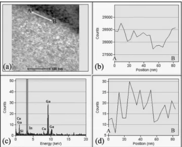
Figure2共a兲shows a low magnified HAADF-STEM im-age of the specimen. The dark area in the upper right corner can be disregarded, that is, where epoxy resin used for the EM sample preparation was placed. EDX analysis was per-formed using a probe size of ⬃0.5 nm along the line indi-cated in Fig.2共a兲, which was a detecting area with a width of ⬃1 nm. The line is parallel to the edge of the specimen, or the basal plane of the GaN, settled just above a SiNxlayer
共which is described below and in Fig.4兲. Figure2共b兲shows the HAADF-STEM intensity profile along the line in Fig. 2共a兲. Figure2共c兲reproduces the averaged EDX spectrum ac-quired from that line. A weak emission from Si was detected together with a very strong emission from In and strong
emissions from Ga. The signal for Cu originated from the specimen support. EDX analysis proves the existence of Si, which was used to form the masks. Figure 2共d兲 shows the intensity profile of In-Lalong the line. HAADF-STEM im-ages give rise to strong contrast dependence on the atomic number Z contrast, unlike conventional TEM images, since they are mainly formed by thermal diffuse scattering of elec-trons or incoherent imaging of elastically scattered electrons.18,19 Therefore, according to the high thermal dif-fuse scattering cross section of In49 atoms compared with Ga31 atoms, the HAADF-STEM intensity of the InGaN is stronger than that of the GaN. In any case, the intensity of the SiNxis the weakest, regardless of x. The peak positions
in the line profiles seem to agree between Figs.2共b兲and2共d兲. Thus, it can be concluded that these peaks indicate the InGaN QDs, and the regions around the valleys between the peaks indicate the GaN, which was deposited as a barrier layer 关see the illustration in Fig. 4共c兲兴. Both the HAADF-STEM intensity and In-Lintensity are very weak around the positions of 20 and 60 nm, where SiNx masks might have
been placed.
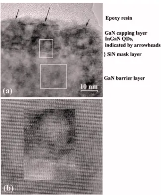
Figure 3 shows nanoanalysis along the line parallel to the c axis. The HAADF-STEM intensity shown in Fig. 3共b兲 increased, as a whole, with the distance from the edge, which can be ascribed to the increase of the specimen thickness. Although it is difficult to determine what corresponds to all the HAADF-STEM peaks observed, at least we can ascertain that the first peak共around the position of 20 nm兲 and the last one共around the position of 60 nm兲 are from the InGaN lay-ers because the In intensities are high, as shown in Fig.3共d兲. The width of the space between these InGaN layers is about 40 nm, which is the evaluated thickness for the GaN barrier layer that was deposited at the nominal thickness of 100 nm. In Fig.4 are shown the two cross-sectional highly mag-nified HAADF-STEM images near the specimen edge. The line indicated by the arrowhead in Fig. 4共a兲 or 4共b兲 is the projection of a SiNx layer, where SiNx mask islands were
FIG. 2. 共a兲 HAADF-STEM image in which the area line scanned for EDX is indicated.共b兲 HAADF-STEM intensity profile along the line A-B shown in共a兲. 共c兲 EDX spectrum. 共d兲 Indium Lintensity profile along the line A-B in共a兲.
deposited on the共0001兲 plane of the underlying GaN barrier layer. The dark contrast of the line is due to the small thermal diffuse scattering cross section of Si14 共and N7兲. The nanoanalysis shown in Fig. 2was performed along the area around this line. From the thickness of the dark line, the height of the SiNxmasks is roughly estimated to be less than
2 nm.
The bright triangles marked by Q in Fig. 4共b兲, which resemble peaks in a mountain chain, should be InGaN QDs. The height of the QDs is estimated to be several nanometers, which is not in disagreement with the results from Tu et al.17 The edges of the triangles could be the兵101¯1其 surfaces of the QDs. Recently, Shiojiri et al.20 proposed an explanation for the formation of V defects, which are formed in multiple InGaN / GaN QW layers grown at temperatures as low as 800– 850 ° C. These V defects, which are empty pyramidal pits with a thin six-walled structure with InGaN / GaN兵101¯1其 QWs, often nucleate on threading dislocations共TDs兲 crossed with the InGaN QWs just above the underlying GaN:Si layer. It is known that the growth rate of the兵101¯1其 surfaces of GaN crystals decreases with decreasing temperature, while the growth rate of the 共0001兲 surface increases.21 Shiojiri et al. took into account this crystal habit and a
mask-ing effect of In atoms, which were trapped and segregated in the strained field around the core of the TD, and then sug-gested that if a mask disturbing the 共0001兲 layer growth is placed at a low temperature, the resulting crystals exhibit 兵101¯1其 facets. The same mechanism is applicable to the growth of QDs. The InGaN was deposited at the low tem-perature of 800 ° C to avoid the low sticking coefficient of In atoms at high growth temperatures. Then the QDs grew as small island crystals with兵101¯1其 surfaces due to the masking of the SiNx, exhibiting natural crystal behavior at the low
temperature. The structure of the specimen is schematically shown in Fig. 4共c兲. The GaN capping layer, deposited at 1000 ° C, covered the QDs 共and also surfaces of the masks with no deposited QDs兲 and caused the outermost surface of the specimen to develop with the共0001兲 plane, accordingly. Figure 5共a兲 shows a HRTEM image near the specimen edge, where part of the capping layer was removed during the ion milling. QDs that are quite high共indicated by arrow-heads兲 are seen on the SiNx mask layer. The dark contrast
may be caused by the diffraction effect of the high structure amplitude of In and the large lattice strain in the QDs. The HRTEM image reveals that the lattices in the QDs were co-herently connected with the GaN lattice in the capping layer, although they were strained. The rectangular frame in Fig. 5共a兲 encloses an area containing the SiNx layer, and the
square frame encloses an area in the GaN barrier layer. In Fig.5共b兲, the former area is the inset on the latter area. The images show that the area to be regarded as the SiNxmask
surely has a heavily strained lattice, but they do not allow us to determine the crystal structure or the composition x of the SiNx.
FIG. 3. 共a兲 HAADF-STEM image in which the area line scanned for EDX is indicated.共b兲 HAADF-STEM intensity profile along the line A-B shown in共a兲. 共c兲 EDX spectrum. 共d兲 Indium Lintensity profile along the line A-B in共a兲.
FIG. 4. 共a兲 HAADF-STEM image near the top of the specimen. 共b兲 High-magnified HAADF-STEM image. White arrowheads indicate SiNxlayers.
Q, InGaN QDs.共c兲 Schematic cross section of the specimen.
FIG. 5.共a兲 HRTEM image near the top of the specimen. 共b兲 Enlarged image of the area enclosed by the square in共a兲, which insets the enlarged image of the area enclosed by the rectangle.
IV. CONCLUSION
We performed cross-sectional analysis of a sample with three-dimensional 共3D兲 InGaN QDs by high-angle annular dark-field共HAADF兲 scanning transmission electron micros-copy共STEM兲, high-resolution transmission electron micros-copy 共HRTEM兲, and energy dispersive x-ray spectroscopy 共EDX兲. Since the InGaN QDs or InGaN nanosized island crystals were randomly distributed on the masked共0001兲 sur-face of the underlying GaN crystal, it was difficult to resolve individual QDs by overlapping, even in the ion-thinned specimen. The following is a summary of the experiment. 共1兲 The sample consisted of an ultrahigh density of InGaN
QDs grown at a reactor temperature of 800 ° C on the 共0001兲 surface of an underlying GaN layer that was par-tially covered with a SiNx masks. Metal organic vapor
phase epitaxy共MOVPE兲 was used for the sample prepa-ration, and the specimens for cross-sectional EM analy-sis were prepared by mechanical polishing, followed by ion milling.
共2兲 The SiNxmasks were confirmed by Si emission in the
EDX spectrum and observed as a dark line in HAADF-STEM image. The height of the SiNxmasks was roughly
estimated from the thickness of the dark line to be less than 2 nm. In HRTEM images, the SiNx masks had
heavily strained lattices, but the crystal structure and the value of x could not be determined from the lattice im-age.
共3兲 The InGaN QDs were observed as bright triangles in the HAAADF-STEM images. The height of the QDs is es-timated to be several nanometers. The edges of the tri-angles, which were the surfaces of the QD, were as-sumed to be兵101¯1其 planes by analogy with the behavior of V defects, which form in multiple InGaN / GaN quan-tum wells deposited at temperatures of 800– 850 ° C. This HAADF-STEM observation of the InGaN QDs was supported by EDS qualitative nanoanalysis and HRTEM. The lattices of the QDs in the HRTEM images were strained as compared to the underlying and the capping GaN layers.
共4兲 The GaN capping layer, deposited at 1000 °C, covered the whole QD layer and masks and caused the outermost
plane of the specimen to have a共0001兲 surface. HRTEM observation showed that the lattice in the GaN was very coherently connected with the lattices of the InGaN QDs.
ACKNOWLEDGMENTS
We thank Dr. C. C. Chuo for discussion and also Z. H. Lee for assistance in MOCVD growth, which was financially supported by the Ministry of Economic Affairs of Taiwan, R.O.C., under Project No. 5301XXN300.
1S. Nakamura, T. Mukai, M. Senoh, S. Nagahama, and N. Iwasa, J. Appl. Phys. 774, 3911共1993兲.
2Y. Narukawa, Y. Kawakami, M. Funato, S. Fujita, S. Fujita, and S. Naka-mura, Appl. Phys. Lett. 70, 981共1997兲.
3T. Takeuchi, H. Takeuchi, S. Sato, H. Sakai, and H. Amano, Jpn. J. Appl. Phys., Part 2 36, L177共1997兲.
4K. P. O’Donnell, R. W. Martin, and P. G. Middleton, Phys. Rev. Lett. 82, 237共1999兲.
5P. Riblet, H. Hirayama, A. Kinoshita, A. Hirata, T. Sugano, and Y. Aoyagi, Appl. Phys. Lett. 75, 2241共1999兲.
6K. Watanabe et al., Appl. Phys. Lett. 82, 715共2003兲.
7J. M. Gérard, O. Cabrol, and B. Sermage, Appl. Phys. Lett. 68, 3123 共1996兲.
8S. Keller, B. P. Keller, M. S. Minsky, J. E. Bowers, U. K. Mishra, S. P. DenBaars, and W. Seifert, J. Cryst. Growth 189/190, 29共1998兲. 9H. Hirayama, S. Tanaka, P. Ramvall, and Y. Aoyagi, Appl. Phys. Lett. 72,
1736共1998兲.
10K. Tachibana, T. Someya, and Y. Arakawa, Appl. Phys. Lett. 74, 383 共1999兲.
11G. T. Liu, A. Stintz, H. Li, K. J. Malloy, and L. F. Lester, Electron. Lett.
35, 1163共1999兲.
12B. Daudin, F. Widmann, G. Feuillet, Y. Samson, M. Arlery, and J. L. Rouvière, Phys. Rev. B 56, R7069共1997兲.
13B. Damilano, N. Grandjean, F. Semond, J. Massies, and M. Leroux, Appl. Phys. Lett. 75, 962共1999兲.
14B. Damilano, N. Grandjean, S. Dalmasso, and J. Massies, Appl. Phys. Lett. 75, 3751共1999兲.
15C. Adelmann, J. Simon, G. Feuillet, N. T. Pelekanos, and B. Daudin, Appl. Phys. Lett. 76, 1570共2000兲.
16S. Tanaka, S. Iwai, and Y. Aoyagi, Appl. Phys. Lett. 69, 4096共1996兲. 17R. C. Tu et al., Jpn. J. Appl. Phys., Part 2 43, L264共2004兲.
18S. J. Pennycook and P. D. Nellist, Impact of Electron and Scanning Probe Microscopy on Material Research共Kluwer, Dordrecht, 1999兲, pp. 161–
207.
19M. Shiojiri and H. Saijo, J. Microsc. 223, 172共2006兲.
20M. Shiojiri, C. C. Chuo, J. T. Hsu, J. R. Yang, and H. Saijo, J. Appl. Phys.
99, 073505共2006兲.
21K. Hiramatsu, K. Nishiyama, A. Motogaito, H. Miyake, Y. Iyechika, and T. Maeda, Phys. Status Solidi A 176, 535共1999兲.