Tunneling Induced Electroluminescence from
Metal-Oxide-Semiconductor Structure on Silicon
*chingFuh Lin *a
CheeweeLiu, Miin-Jang Chen a Ming-Hung Lee, and 1-Cheng Lin
Department ofElectrical Engineering, National Taiwan University, Taipei, Taiwan, ROC
aalso
with Graduate Institute of Electro-Optical Engineering
ABSTRACT
Silicon is the most important semiconductor material for electronics industry. However, its indirect bandgap makes it
hardly emit light, so its applications in optoelectromcs are limited. Many efforts had been devoted to converting silicon to
light-emitting materials, including porous silicon-based devices, nanociystalline Si, and so on. In this work, we report
electroluminescence on silicon with simple metal-oxide-semiconductor (MOS) structure. The thin oxide is grown by
well-controlled rapid thermal oxidation. With extremely thin oxide, significant tunneling current flows through the MOS structure as the metal is properly biased. The tunneled electrons could then occupy the upper energy levels more than the thennal-equilibnmn situation. Then luminescence occurs when they have radiative transition to lower energy states. For low biased voltages, the emission occurs around 1 150 rim, approximately corresponding to the Si bandgap energy. For large applied voltages, the emission shifts to longer wavelengths and becomes voltage-dependent MOS structures fabricated on both p-type and n-type silicon exhibit electroluminescence. This is significant because the fabrication of those MOS structures is compatible with CMOS electronics. Therefore, the MOS EL devices provide a particular advantage over other types of luminescence on silicon. The details of the electroluminescence and its physical reason are
reported and discussed.
Keywords: Electroluminescence, silicon, metal-oxide-semiconductor, CMOS. rapid thennal oxidation, radiative transition, tunneling current.
1. INTRODUCTION
The mature technology of Si had made it the most important material for mtegrated-cfrcuit (IC) industry. The popularity
and low-cost Si technology had caused IC industry to penetrate many aspects of human life after 1950s. Therefore, many
efforts had also been devoted to making Si useful for optics and optoelectromcs, hoping to extend Si technology to more
areas. There had been some achievements in the applications of Si processing technology to the fabrication of
optoelectromc components. They include detectors, waveguides, 'modulators,2wavelengthdemultiplexers, and
micro-optics. Even with those components, integration of optoelectronics into Si-based technology is still limited because light emission directly from Si material is not feasible. The main obstacle is due to the mdirect-bandgap nature, which causes
light emission from Si to be extremely challenging.
1.1. Review of Luminescence from Silicon
Many groups had searched ways to overcome this obstacle. Those efforts include porous-silicon-based devices, doping
impurity into Si, 810 Sit-implanted
Si02, "
12 ffloyingSi with Ge or Sn, '
14 nanocrystallineSi, '
16 orquantum-confinement structures, 'depositionofpolymer on Si substrates, 18 of GaN on Si substrates, 19,20 andso on. Porous
Si mostly emits visible light Its physics of luminescence had been attributed to surface states, surface species, and quantum confinement. 21 The exact mechanisms are still not well known. Doping impurities into Si utilizes luminescence centers like Er or other ions. The low solid solubility and small interaction cross section are serious hurdles for such
applications. Alloying Si with Ge or Sn and nanocrystalline Si are based on the theory and engineering of band structures, trying to modify the indirect-bandgap nature of Si to direct bandgap. Its success very depends on the growth technology of
epitaxial materials. The growth of GaN on Si substrates also relies on the growth technology of lattice-mismatched
materials. Deposition of polymer on Si substrate is a simple way, but the polymer cannot endure high-temperature process
and so possibly limits its compatibility with current IC technology. In the above approaches, either the Si material is
significantly modified or other material is used for light emission, so the ongrnal conduction-band minimum and
band maximum of Si is not used for radiative recombination, leading to the light emission shifting away from the Si
bandgap energy. Those modifications are mostly complicated or incompatible with current Si-based IC technology.
1.2. Our Approach
In this work, we propose a new way for electroluminescence from Si without significanfly modifying the Si material
property. The electroluminescence is based on the metal-oxide-semiconductor (MOS) structures on Si. The oxide is grown
by the well-controlled rapid thermal oxidation (RTO). The emission corresponds to bandgap energy and longer
wavelengths. Their physical reasons will be discussed. Such MOS structures with the RTO grown oxide are particularly advantageous over other types of luminescence on Si because their processing steps are completely compatible with the IC fabrication. MOS on both p-type and n-type Si exhibits the electroluminescence, so it could be directly integrated with the
popular CMOS technology.
Conventional MOS structures are used in field-effect transistors for isolating the gate contact from the conducting
channels. It is important to have good insulation property in the oxide so that no current flows through the oxide. In our case, in order to have electroluminescence, significant current has to flow through the oxide. This could be achieved by
two ways. First, the oxide layer contains lots of defects or ions. Second, the oxide is so thin that significant carriers could tunnel through quantum mechanically. The first one had been investigated recently using Ag/SiO2/Si structure or similar MOS structures with native oxide.22'23 Visible electroluminescence (EL) had been reported from such structures. However,
the native oxide usually contains deficient defects and its property strongly relies on the forming environment. 24As
a
matter of fact, the luminescence is due to luminescent centers or oxygen deficient defects in the native oxide. In this work,
we adapt the second approach. The oxide is grown by well-controlled RTO and is only a few nanometers to allow
tunneling current. The high-temperature process of RTO makes the grown oxide very stable and immune to environmental variations after the growth.
2.1. Oxide Growth
2. SAMPLE PREPARATION
The MOS structures used in the study were grown on (100) Si wafers. Both n-type and p-type wafers had been used. The resistivity of the 100 nun n-type and p-type wafers is 1-10 ohm-cm and 1-5 ohm-cm, respectively. The gas flows in RTO
are 500 sccm nitrogen and 500 sccm oxygen. Ultra pure gases were used in the growth chamber to eliminate possible
formation of undesired ions in the oxide. Several samples had been grown by RTO. The first one has 2.3 mu oxide grown on the p-type Si wafer. The second one has 3.3 urn oxide grown on the n-type Si wafer. Their growth conditions are both at the pressure of 500 mbar and temperature of 900 °C. The thickness was measured by ellipsometry and confirmed by x-ray
reflectivity. The third one has the oxide grown on the p-type wafer and the forth one has the oxide grown on the n-type
wafer. Their growth conditions are changed to under reduced pressure and at temperature of over 1000 °C. The oxide also has the thickness around 3 nm.
2.2. Metalization
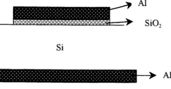
Si
Fig. 1 A schematic of MOS stnicutres Si02
The Aluminum metal was then deposited on top of the oxide by evaporation right after RTO in order to prevent the regrowth of native oxide as a result of the exposure to atmosphere. After the deposition of the Al on the oxide, another metalization for ohmic contact was performed on the other side of the Si wafer. Then on the oxide side, patterns with
circular areas and straight lines of Al pads were formed by chemical etching. The circular areas have diameters of2.5 mm.
3.1 Electrical characteristics
3. EXPERIMENTAL RESULTS
Fig. 2 shows a typical cw J-V curve of the MOS on n-type Si without cooling. This curve was measured on the device with
2mm-diameter Al pads. The voltage was applied between the metal on top of oxide and Si. This curve shows fair
rectification characteristics. For the MOS on n-type Si, significant current could flow through the oxide when this metal is
positively biased. On the other hand, significant current is measured when the metal on top of oxide is negatively biased for the MOS on p-type Si. Adapting the terminology of conventional diodes, we name this condition with large current
flow as forward bias and the opposite bias as reversed bias. The MOS on p-type Si has a similar J-V curve except that its
turn-on voltage is larger because the Al Fermi-level (E)iscloser to the valence band of Si than the conduction band.
400. E
20.
0,
voltage (V)
Fig. 2 A typical J-V curve for MOS with thin oxide on n-type silicon.
The low-temperature J-V curve was also measured. As shown in Fig. 3, the temperature does not have strong
influences on the J-V characteristics, indicating that the current flow is mainly caused by the tunneling effect.
3.2. Electroluminescence 2000 1800
.
1600 1400 1200.
1000 800 600 400 200Fig. 3 J-V curves for MOS with thin oxide at different temperatures.
Under the forward bias, the two samples with oxide grown at the pressure of 500 mbar exhibited luniinescence that could be clearly observed through an JR-viewer. The emission mainly emitted from the periphery of the circular area because the
metal pads were made of thick aluminum. Therefore, only a small portion of light was measured. The shape is like the total eclipse of sun. The eclipse-like luminescence could be clearly observed through the JR-viewer even with a current
density as low as 0.67 A/cm2. Under the reversed bias, no luminescence was observed.
-Lo
b i'.o 2.0C
C
The emission spectra were measured using a monochromator from the circular area of 2.5 mm-diameter Al pad on top of
oxide. Figs. 6 (a) and (b) show the measured spectra with the emission centered around 1 150 rim and 1 180 nm for the
MOS on p-type and n-type Si, respectively, under cw operation without cooling. Both correspond to the bandgap energy Eg of Si slightly above the room temperature. Because the MOS on n-type Si has a larger current than the MOS on p-type Si under the same bias, more ohmic heat is generated, leading to the longer wavelength for the MOS on n-type Si. These
spectra correspond to Region I of the L-I curve in Fig. 5. Only the two samples with oxide grown at the pressure of 500 3.2.1 L-I Characteristics
Fig. 4 shows the measured L-I curve (output power vs. injection current) for the MOS structures on n-type Si under cw operation without cooling under the low applied voltage. As the applied voltage increases, the L-I curve behaves
differently, as shown in Fig. 5. This curve is measured for the MOS on p-type Si. The L-I curve consists of two different
parts, regions I and II. They correspond to the applied voltage approximately below and above 5 V. respectively. For
region I, the curve shows a superlinear increase of the output power with the injection current. in region II, abnormal L-I
characteristics are observed. The MOS on n-type Si has similar behaviors except that region II occurs for the applied voltage approximately above 10 V. The reason can be explained as follows. Because the MOS on n-type Si has a larger current under the same bias, most of the voltage drops across the thick Si substrate instead of the oxide. As a result, the
applied voltage appears to be larger.
I0
5
200 600
Injection current (mA)
Fig. 4TheL-I curve of the electroluminescence from the MOS on n-type Si under low applied voltage.
1.0
0.5
250 500
3.2.2 Emission Spectra
Injection current (mA)
Fig. 5 The L-I characteristics of the electroluminescence from the MOS on p-type silicon. Region I: below dash line; region II: above dash line.
mbar exhibited the emission at bandgap energy. The other two samples with oxide grown at reduced pressure shows no
emission at this wavelength at all.
(a) (b)
Fig. 6 The measured spectra under cw operation without cooling from the MOS on (a) p-type Si (b) n-type Si.
By increasing the applied voltage, the emission power initially increases with the injection current, but then gradually decreases as the voltage approaches 5 V or 10 V for MOS on p-type Si or n-type Si, respectively. When the
applied voltage increases beyond 5
V
or 10 V, the luminescence near 1150 ma completely vanishes and then luminescenceat longer wavelengths appears. The measured spectra are shown in Fig. 7 at different applied voltages for the MOS on
p-type Si. These spectra correspond to the abnormal characteristics of region II of the L-I curve in Fig. 5.Asshown in Fig. 7, when the applied voltage further increases, the spectra move toward shorter wavelengths, but are still longer than 1200 nm.
The measured spectral range is limited by the lnGaAs detector. The entire spectra should extend beyond 1700 nm. All of
the four samples exhibited such voltage-dependent emission beyond 1200 nm.
Fig. 7 The measured spectra under cw operation without cooling for region II in Fig. 5.
3.2.3 Discussion on Emission Spectra
Different from other reports, 22,23, 25 our devices exhibit no visible luminescence. The previously reported visible
luminescence from the MOS with native oxide 25,26
probably due to luminescent centers or oxygen deficient defects in the native oxide. In our devices, because the oxide was grown by the well-controlled RTO, it should have much less
defects than the native oxide. Thus visible luminescence is not observed. The C-V measurements further confirm that there is negligible interface trap in the oxide or near the interface of the oxide and Si. The different lu.minescence in our devices
1000 1200 1400
Avelength(nm)
1600 1200 1400
veIength (nrrj
should be due to different mechanisms involved. The mechanisms for the emissions near bandgap energy and longer
wavelengths will be discussed separately in the following.
4.1. Emissionat Bandgap Energy
4. THEORETICAL EXPLANATION
The discussion for the emission around Eg is based on the MOS on p-type Si only because the physical reason for the
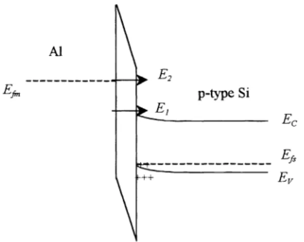
MOS on n-type Si is siniilar. A schematic of the band diagram shown in Fig. S is used for the explanation. For the MOS on
p-type Si, E
increaseswith the forward bias. Electrons then tunnel from metal to Si and holes tunnel vice versa. Themajor contribution of current comes from the tunneling of electrons instead of holes for the MOS on p-type Si. 27
Increasingthe negative bias at the metal side causes Efi,,toshift up to the conduction band edge (Ec).Thenthe tunneling
current significantly increases because the tunneling electrons could fill in many states in the conduction band. On the other hand, the negative bias of metal causes the band of the p-type silicon to bend up near the SiISiO2 interface, as
schematically shown in Fig. 8. A potential well for hole confinement is then formed. leading to the accumulation of holes
near the interface. Consequently, huge population of the holes and the tunneling electrons simultaneously appear in the
well region.
Fig. 8 A schematic of the band diagram with the metal of the MOS on p-type Si negatively biased.
In addition to the simultaneous appearance of many electrons and holes in the same region. momentum
conservation is also necessary to have radiative recombination. This could not, in general, happen in the indirect-bandgap material. However, if there is any lattice disorder near the SiISiO2 interface, 28therequirement of momentum conservation
could be relaxed. In the formation of oxidation during RTO, small-scale roughness at the interface could be possibly
formed to provide extra momentum required for radiative recombination for elections and holes.
Because the Si atoms on the top surface of the (100) Si wafer have their atom spacing less than the total bonding
length of Si-O-Si, not each atom could be chemically bonded with oxygen atoms. Then some Si atoms are not oxidized.
Those atoms are named as s-Si for simple explanation later. Similarly, the others that are chemically bonded with oxygen
atoms are named as o-Si. Because the s-Si atoms on the top surface are not oxidized, they are still part of the
semiconductor. On the other hand, they are closer to metal than other Si atoms in the semiconductor below the top layer,
so more electrons tunnel to the region of s-Si atoms. Therefore, many tunneling electrons are localized around the s-Si
atom in the direction parallel to the interface, causing their wavefunction to be laterally localized. Then their wavefunction in the momentum space will have a large spread in the corresponding direction according to the uncertainty principle. The extra momentum required for the electron-hole radiative recombination is thus provided.
In the extreme case, each s-Si atom on the top surface is surrounded by o-Si atoms, so the lateral localization is in the range less than the lattice constant As a result, the electron tunneling to s-Si atom has a spatial wavefunction localized to within the lattice constant a. Its Fourier-transformed wavefunction in k-space could then extend to beyond 2ir Ia,which
is sufficient to compensate for conduction-band minimum near the X point. Therefore, electron-hole radiative
recombination is largely enhanced.
Those samples with the thin oxide grown by RTO at the reduced pressure had also been measured. Because of the thin oxide, significant current was still obtained when they were forward biased. The reduced pressure causes Si atoms on
Al
p-type Si
E
E
the top surface of Si wafer to be less oxidized. As a result, more s-Si atoms are neighboring together instead of being laterally isolated by o-Si atoms. Because the corresponding spatial wavefunction of tunneling electrons is less confined, the wavefucntion in k-space has less spread, leading to insufficient momentum for the compensation. Therefore, those samples exhibit no emission corresponding to Si bandgap energy although they also demonstrate behaviors of diodes.
They also have no visible luminescence, indicating that the oxide grown at reduced pressure contains negligible defects to work as luminescent centers.
The emission energy corresponding to 1 150 mn and 1 180 nm is slightly less than Si bandgap energy at the room
temperature. They could be explained by the following reasons. First, the increasing carrier density29mightresult in the bandgap shrinkage and so the red shift. Second, the interruption of Si periodical structure at the interface causes band bending and the bandgap hrink3° Third, the large injection current leads to significant ohmic heat and temperature rise, so the bandgap energy is reduced. The ohmic heat could also explain the MOS on n-type Si emitling light at a longer
wavelength because it has a larger current under the same bias.
4.2. Emission at Wavelengths Longer Than 1200 nm
When the applied voltage increases to be much larger than the Fermi-level difference, E,,moves far above Ec, as
schematically shown in Fig. 9. The electrons with energy E1nearEcthen see an increased potential barrier, so their tunneling probability is reduced. On the other hand, the electrons with their energy E2nearEr,,,haveincreased tunneling
probability as a result of the strongly tilted potential barrier. Those electrons tunnel into the high-energy states of the conduction band. Therefore, radiative recombination corresponding to Eg is reduced. The emission conesponding to the
bandgap energy therefore disappears, as shown in Fig 7.
Al
p-type Si
Fig. 9 A schematic of the band diagram with the metal ofthe MOS structure negatively biased for Efrfarabove Ec.
Fig.7 also shows that the emission shifts to longer wavelengths at large applied voltages. This emission was
observed for all of the four samples described in Section II. The reasons for such emission are discussed as follows. First,
it might be possibly due to the interfacial states in the grown oxide. However, the C-V measurement indicates only very
small amount of interface Imp in the oxide, implying that the interfacial states are probably not significant. In addition, the spectrum is voltage-dependent, so the mterfacial states should not be the main cause. Second, black-body radiation might also be the reason. To identify if the emission is caused by black-body radiation, similar measurements had been done with the sample cooled. Under the same bias condition, the emission near 1600 nm for the sample cooled down to 10 K is even stronger than at 300 K, indicating that black-body radiation alone could not explain the emission well. Third, as E5,,moves
up further, as shown in Fig. 9, electrons tunnel to the states far above Ec.Thosehot carriers could then relax to lower energy states, e.g. E2—>E1,bydirect or phonon-assisted inter-conduction-band radiation. 31,32 Agradual shift of spectrum
from 1200 nm to beyond 1300 rim with mcreasmg applied voltages for MOS on n-type Si had been observed, indicating
the possibility of the third mechanism. As discussed before, at large applied voltages, the number of tunneled carriers with
energy near band edge is reduced, while more carriers tunnel into the high-energy states. Therefore, emission
Although the above discussion is for the MOS on p-type Si, the physics of the MOS on n-type Si are similar. The only difference is that the major role becomes the hole instead of the electron.
Different from the physics involved in the emission at bandgap energy, the emission at longer wavelengths is not due to the surface roughness. Therefore, all of the four samples should exhibit the emission characteristics regardless of the growth pressure, as demonstrated experimentally.
5. CONCLUSION
In conclusion, room-temperature electroluminescence from the simple MOS structure on silicon is observed. The thin
oxide grown by the well-controlled RTO provides the mechanism for carrier tunneling quantum mechanically. The MOS then behaves like light emitting diodes. Under low applied voltages, the emission wavelength is around 1 150 nm, which
approximately corresponds to Si bandgap energy. This emission is attributed to the roughness generated at the Si/Si02
interface during RTO. This roughness accounts for the compensation of extra momentum required in radiative
recombination in indirect-bandgap materials. When the applied voltage is increased to much larger than the Fermi-level
difference between the metal and Si, the emission wavelength becomes longer than 1 150 nm and voltage-dependent. The emission is possibly caused by direct or phonon-assisted c-c or v-v radiative transition.
ACKNOWLEDGEMENTS
This work is supported in part by National Science Council, Taipei, Taiwan, R.O.C. under the contract No.
88-2218-E-002-004, No. NSC88-2215-E-002-021, andNo. N5C2112-M-002-038.
REFERENCES
1. N. Takato, K. Jinguji, M. Yasu, H. Toba, and M. Kawachi, JEEEJ. Light-wave Technol. 6, pp. 1003-1010, 1988. 2. G. V. Treyz, PG. May, and J.-M. Halbout, Appi. Phys. Lett. 59, pp. 771-773. 1991.
3. M. L. Cohen and T. L. Bergstresser, Phys. Rev. 141, pp. 789-796, 1966.
4. M. C. Wu, L.-Y. Lin, S.-S. Lee, and K. S. J. Pister, Sensors andActuators A 50, pp. 127-134, 1995. 5. L. T. Canham,Appl. Phys. LeLt. 57, pp. 1046-1048, 1990.
6. N. Koshida and H. Koyama, Appi. Phys. Lett. 60, pp. 347-349, 1992.
7. S. Lazarouk, P. Jaguiro, S. Katsouba, G. Masini, S. La Monica, G. Maiello, and F. Ferrari, Appl. Phys. Lett. 68, pp. 2108-2110, 1996.
8. H. Ennen. J. Schneider, G. Pomerenke, A. Axmann,Appl. Phys. Lett. 43, pp. 943-945, 1983.
9. G. Franzo, F. Priolo, S. Coffa, A. Polman, and A. Carnera,Appl. Phys. Lett. 64, pp. 2235-2237, 1994.
10. M. Matsuoka, and S. Tohno, Appi. Phys. Lett. 71, pp. 96-98, 1997.
11. L. S. Liao, X.-M. Bao, X.-Q. Zheng, N-S. Li, andN.-B. Min,Appl. Phys. Lett. 68, pp. 850-852, 1996.
12. W. Skorupa. R. A. Yankov, I. E. Tyschenko. H. Frob, T. Bohme. and K. Leo, App!. Phys. Lett. 68, pp. 2410-2412, 1996.
13. S. Oguz et al., Appi. Phys. Lett. 43, pp. 848-850, 1983.
14. C. W. Liu, J. C. Sturm, Y. R. J. Lacroix, M. L. W. Thewalt, and D. D. Ferovic, Mat. Res. Soc. Symp. Proc. 342, pp. 37-42,1994.
15. S. Schuppler, S. L. Friedman. M. A. Marcus, D. L. Adler, Y.-H. Xie, F. M. Ross, Y. J. Chabal, T. D. Harris, L. E. Brus, W. L. Brown, B. E. Chaban. P. F. Szajowski, S. B. Christman, and P. H. Citrin, Phys. Rev. B 52, pp.
4910-4925,1995.
16. D. B. Geohegan. A. A. Puretzky, G. Duscher, and S. J. Pennycook, App!. Phys. Lett. 73, pp. 438-439, 1998.
17. F. Buda et al., Phys.Rev. Lett. 69, pp. 1272-1275, 1992.
18. D. R. Baigent, R. N. Marks, N. C. Greenham, R. H. Friend, S. C. Moratti, and A. B. Holmes, App!. Phys. Lett. 65, pp. 2636-2638,1994.
19. R. Birkhahn and A. J. Steckl,Appl. Phys. Lett. 73, pp. 1700-1702, 1998.
20. M. Garter, J. Scofield, R. Birkhahn, and A. J. Stecki, Appi. Phys. Lett. 74, pp. 182-184, 1999.
21. Zhanghua Wu, Tomonobu Nakayama, Shan Qiao, and Masa.kazu Aono. Appl.Phys. Lett. 74, pp. 3842-3844, 1999. 22. Y. Q.Wang,T. P. Zhao, J. Liu and G. G. Qin,Appl. Phys. Lett., 74, pp. 3815-3817, 1999.
23. J.Yuan and D. Haneman,J.Appi. Phys. 86, pp. 2358-2360, 1999.
24. ULSItechnology, edited by Cluing, C. Y. and Sze, S. M., New York, McGraw-Hill, 1996.
25. G. F. Bal, Y. Q.Wang,Z. C. Ma, W. H. Zong, and G. G. Qin,J. Phys.: Condens. Matter 10, L717-L721,1998. 26. D. L. Griscom, I C'eram. Soc. Jpn. 99, 899, 1991.
27. C. W. Liu, M. H. Lee, C. F. Liii, I. C. Liii, W. T. Liu, and H. H. Lin, 1999 IEEE International Electron Devices
Meeting, Paper 31.3, Washington, D. C., December, 1999.
28. M. Jaros and A. W. Beavis,Appl. Phys. Lett. 63,pp.669-67 1, 1993.
29. H. C. Casey, Jr. and M. B. Panish, Heterostructure Lasers, Part A, Academic Press, Orlando, 1978. 30. S. M. Sze, Physics of Semiconductor Devices, 1981.
31. J. Bude, N. Sano, and A. Yoshii, Phys. Rev. B45, pp.5848-5856, 1992.