Parallel Scrambler for High-Speed Applications
Chih-Hsien Lin, Chih-Ning Chen, You-Jiun Wang, Ju-Yuan Hsiao, and Shyh-Jye Jou
Abstract—In order to improve the speed limitation of serial
scrambler, we propose a new parallel scrambler architecture and circuit to overcome the limitation of serial scrambler. A very sys-tematic parallel scrambler design methodology is first proposed. The critical path delay is only one D-register and oneXORgate of two inputs. Thus, it is superior to other proposed circuits in high-speed applications. A new DET D-register with embedded XORoperation is used as a basic circuit block of the parallel scram-bler. Measurement results show the proposed parallel scrambler can operate in 40 Gbps with 16 outputs in TSMC 0.18- m CMOS process.
Index Terms—Parallel scrambler, register,XOR.
I. INTRODUCTION
I
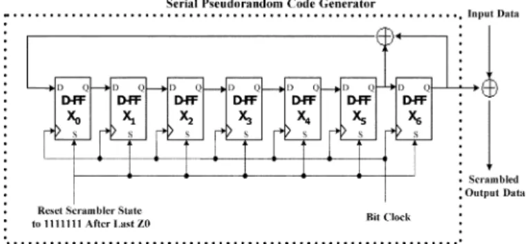
N DIGITAL transmission systems, there are always scram-blers to scramble the transmission data. In general, multi-ples of base rate signals are multiplexed and then scrambled be-fore transmission which is descrambled and demultiplexed after reception. Scrambling used to be done serially. Standard like IEEE802.3ae (10-Gbps Ethernet) describes the functional dia-gram as a 7-bit series synchronous frame scrambler. The gen-erated pattern is a maximal length sequence (m-sequence) of (in this case ). The scrambler diagram shown in Fig. 1 shall generate a continuous stream of output bits at the same rate as the transmitted bit rate ( ).Nevertheless, as the operating frequencies of transmission systems grow beyond gigabits per second, serial scrambling techniques were no longer applicable. For example, in 10-Gbps Ethernet or 40-Gbps fiber transmission, with serial scrambling, this would mean working at frequency of 10/40 GHz which is not feasible with today’s silicon-based CMOS integrated cir-cuits. The requirement of high working frequency can be re-solved by using parallel scrambling techniques [1]–[5] to enable the scrambling process at the low-frequency base rate. Under parallel scrambling, a set of scrambling processes are performed at the base rate, which collectively achieves the effect of se-rial scrambling when the scrambled base-rate signals are multi-plexed to form a transmission-rate signal. A common character-istic of all well-known parallel solutions is that the number of inputs of the modulo-2 adders (XORgates) used in the feedback
Manuscript received March 31, 2004; revised December 1, 2005. This work was supported by the Chip Implementation Center, National Science Council and MOEC of Taiwan, R.O.C. under Grant NSC92-2215-E-008-003 and Grant 92-EC-17-A-07-S1-0001 This paper was recommended by Associate Editor M. Soma.
C.-H. Lin, C.-N. Chen, Y.-J. Wang, and J.-Y. Hsiao are with the Depart-ment of Electrical Engineering, National Central University, Jung-Li City, 320 Taiwan, R.O.C.
S.-J. Jou is Professor in the Department of Electronics Engineering, National Chiao Tung University, Hsinchu City, 300 Taiwan, R.O.C. ([email protected]. edu.tw).
Digital Object Identifier 10.1109/TCSII.2006.875316
Fig. 1. Circuit diagram of serial scrambler in IEEE802.3ae.
loops of the pseudorandom code generator is more than two for some parallel ports. However, having to process the modulo-2 additions of more than two inputs will lead to an increase in the processing delay and lower the maximum working rate. More-over, in today’s deep submicrometer CMOS process, number of fanouts and interconnect length also become a significant factor that affect the processing delay. Thus, the architecture shall be regular and have less fanouts in the critical path.
In this brief, a very systematic parallel scrambler design methodology and new architecture is proposed. In the fol-lowing, Section II will show the design methodology and procedures to develop parallel pseudorandom code generator used in parallel scrambling. Section III will show the architec-tures, circuits and measurement results. Finally, a conclusion is made.
II. REALIZATION OFPARALLELPSEUDORANDOM
CODEGENERATOR
There are various publications [1]–[5] in which parallel scrambling techniques are described. They allow any number of parallel bits to be generated in each clock cycle. To realize the parallel pseudorandom code generator, the minimized circuit complexity required D-registers and XOR2s (two inputs) [2], [5] for serial scrambler with a singleXOR2. However, the
XOR gates in the critical path for some of the parallel ports have more than two inputs. In the following, we will show the procedures that transform the serial scrambling to parallel scrambling with only a XOR2 gate in the critical path of the
parallel ports.
(i) Describe the generating polynomial as
or (1)
where is the generated bits in the time sequence of serial pseudorandom code generator with
for to and to (2) Here, we define as the minimal index of that
and . Also, represents the number of coefficients that to equal 1 (the number of inputs to theXORgates). In applications, is usually two to reduce
circuit complexity.
Example 1: or
where and . Substitute into (2),
we have .
(ii) Determine the number of parallel output port and write the parallel output bits generated in jth output cycle as a
word for to
(3) where is the bit that generated in cycle at port . The initial conditions for are stored in the registers when start-up.
Example 2:
where to represent the initial conditions of the serial pseu-dorandom code generator.
Note that if , we still need registers to store the initial conditions.
(iii) For each bit in , calculate and by using
and modulo .
Recursively apply (3) such that only uses bits in .
Example 3:
where is the word after applying (3) times for some bits in . In this case, the and are two solutions that only use 2 bits in .
(iv) Using the bit operations in as the logic operation in output ports.
Example 4: We can derive the output ports and their
opera-tions as
or
This parallel architecture has the following properties. 1) Any number of parallel outputs can be designed from the
serial scrambler. Recursive equations are derived to do the transformation.
2) If the number of inputs to theXORof the serial scrambler is (two in Fig. 1) then the number of inputs to theXORin the parallel scrambler can also be .
3) By applying recursion (3) different number of times, there are several representations that have the above two properties.
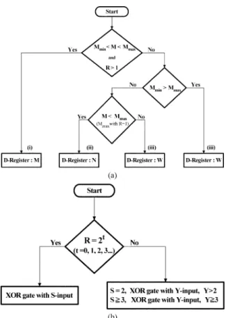
The relationships among , , , and number of iterations ( ) of applying (3) are shown in Fig. 2 and are written in the following propositions.
Proposition A: A parallel pseudorandom code generator with
M parallel outputs has three cases for the number of register used according to the relationships of , and . i) One register at each port and total registers. ii) More than one register at some ports and total registers. iii) More than one D-register at some ports and total registers.
in case iii) of Proposition A depends on the two situations:
1) if and (2)
if . In here .
Proposition B: A parallel pseudorandom code generator with
R equals to power of 2 has the property that each port only con-sists of XOR2 gates.
Example 5: For polynomial , , and are listed in Table I for is power of 2.
Example 6: is another polynomial of maximal length sequence of seven stage. In this case ,
Fig. 2. (a) Total registers required. (b) TotalXOR2 gates required. TABLE I
R, M ANDM FORPOLYNOMIALP (x) = X + X + 1
. For , we have
In , generated at cycle 1 uses in the same cycle, thus it can not be implemented with only one XOR2 gate and one register. Thus, bits in are required to be stored as initial con-ditions
where @ means cascade. With , it consists of fiveXOR2 gates with ten registers for storing initial conditions. However, the critical path is still oneXOR2 gate and one register.
Fig. 3(a) shows a parallel pseudorandom code generator with equals 16 of the serial scrambling shown in Fig. 1 using
Fig. 3. Parallel pseudorandom code generators withM = 16. (a) Maximal fanouts of 5. (b) Maximal fanouts of 3.
Fig. 4. Parallel pseudorandom code generators withM = 16 of P (x) = X11 + X9 + 1 used in IEEE1394.
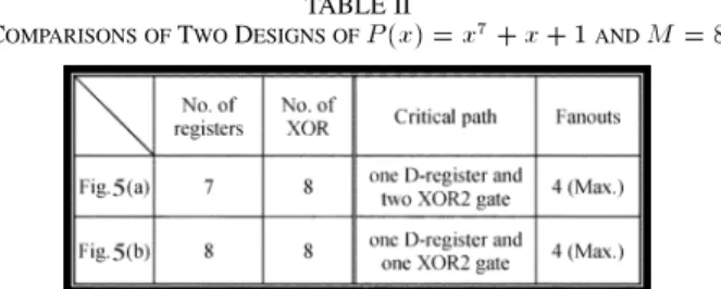
in Example 3. Each output port consists of oneXOR2 gate cas-caded by one register and the number of fan-outs is from 2 to 5. This kind of parallel scrambler architecture is very regular and has the potential for high-speed operation. If maximal number of fanouts is very important, we can try to use in Example 3 to reduce the maximal number of fanouts as shown in Fig. 3(b). As you can see, the maximal number of fanouts is reduced from 5 to 3. Fig. 4 shows another example of used in IEEE1394b. Each output port only consists of oneXOR2 gate cascaded by one register and the maximum number of fan-outs is 5. Fig. 5 shows the example used in Example 6 with five par-allel outputs. Although each port required two registers, the crit-ical path is still oneXOR2 gate and one register. Fig. 6(a) shows the design example proposed in [5, Fig. 4] and Fig. 6(b) shows the one derived here. The comparisons are listed in Table II. Due to the reduction of twoXOR2 to oneXOR2, the proposed
archi-tecture can be used in higher operational speed. III. ARCHITECTURE ANDCIRCUITDESIGN
In the parallel pseudorandom code generator, the basic cir-cuit block isXOR2 gate cascaded by D-register. If single edge triggered (SET) D-registers are used, the operational frequency is . As we know, high-speed clock buffers consume lots of power due to the stringent timing requirement of rise/fall
Fig. 5. Example used in Example 6 with 5 parallel outputs.
Fig. 6. P (x) = X + X + 1 with M = 8. (a) Circuit proposed in [5, Fig. 4 ]. (b) Circuit proposed in this brief.
TABLE II
COMPARISONS OFTWODESIGNS OFP (x) = x + x + 1ANDM = 8
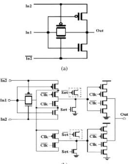
and delay time. Thus, we use double edge triggered (DET) D-register which provides data sampling at both rising and falling edges of clock. In this way, the clock frequency is only half of that used for SET D-register. Fig. 7(a) and (b) shows two conventional DET D-registers [6]. DET-TSPC merges two SET-TSPC D-registers but improves the design by reducing the number of clocked transistor to six instead of eight. It suffers from the same problems of TSPC-based register such as output dip, charge sharing, etc. DET- is a safety design and has low input loading (one pMOS and nMOS) as compared to DET-TSPC (two pMOS and two nMOS). Thus, it is ideally suited for two phase clock systems. The XOR circuit shown in Fig. 8(a) is a frequently used CMOS circuit. The critical path delay is only a pMOS or nMOS. The output is driven by signal source and is not driven by VDD and GND. This is one disadvantage of this XORcircuits. It will cause delay problem if such XOR’s are cascaded. However, in here, no XORs are cascaded so it shall be no problem.
Table III shows the HSPICE simulation results of serial scrambler using the DET-TSPC or DET- cascaded by
XOR2. The technology used is TSMC 0.18- m 1.8-V CMOS process. The operational clock cycle is limited by
(4)
Fig. 7. (a) DET-TSPC. (b) DET-C MOS. TABLE III
PERFORMANCECOMPARISONS OFSERIALSCRAMBLERS
where , , and is the set up time, clock to output delay time of D-register, and delay time of XOR gate. We can reduce by embedding theXOR opera-tion into the master stage of DET- XOR
-DET-as shown in Fig. 8(b). By doing so, not only the number of tran-sistors is reduced by two but the delay path ofXORand set up path of DET- are merged. TheXORoperation can not be merged into the DET-TSPC in the same way and need a much complicated structure. Table III also shows the simula-tion results of the serial scrambler using the proposed circuits. It can work up to 3.6 Gbps (1.8 GHz) and is 1.4 times faster than the conventionalXORcascaded by DET- . By using the proposed XOR-DET- circuit in the parallel scrambler [Fig. 3(a)], because the maximum fan-out number is 5 instead of 2 in serial scrambler, pre-layout simulations show that the op-erational clock can only work at 2.7 Gbps per port.
If a one-dimensional array like the one shown in Fig. 3(a) is implemented, the post-layout simulation shows that it can only work up to 2.4 Gbps. The decreasing of operational speed is due to a long interconnect of several hundreds of micrometers. We carefully redo the layout in a rectangular format (scrambler I) as shown in Fig. 9 to reduce the interconnect length. Post-layout simulation shows that it can work at 2.55-Gbps per port. Parallel
(a)
(b)
Fig. 8. (a)XORcircuit. (b) ProposedXOR-DET D-register.
Fig. 9. Layout of the proposed parallel pseudorandom code generator.
Fig. 10. Test circuit diagram.
scramblers designed by usingXORcascaded by
DET-[Fig. 7(b), scrambler II] are also designed and implemented in a rectangular format. The post-layout simulation results show that the scrambler II can only work up to 1.76-Gbps per port. A test chip is implemented by using TSMC 0.18- m 1.8-V CMOS process for both scrambler I and scrambler II as shown in Fig. 10. A di-vide-by-2 divider is used to have clock signal with 50% duty cycle. Due to the characteristic of the parallel scrambler, it has a periodic pattern every 127 output cycles. So we design a decision circuit that will be triggered each time this pattern is matched. Thus, when the output of the T-FF has a stable clock frequency of , then we know the parallel scrambler can work in . The
Fig. 11. Chip photo.
TABLE IV
CHIPSUMMARY ANDCOMPARISONS
chip photo is shown in Fig. 11. The measurement results are listed in Table IV and quite match the post-layout simulation results. The measured maximum T-FF output frequency is 9.8448 MHz. Thus, the proposed parallel scrambler and new circuits can wok at 40 Gbps. The results show that the proposed circuits can work 1.5 times faster than the conventional one with smaller layout area and less power consumption.
IV. CONCLUSION
A very systematic parallel scrambler design methodology is proposed. The structure of the parallel scrambler is very regular andthecriticalpathdelayisonlyoneD-registerandoneXOR2gate. Moreover, by applying the recursive equations different number of times on different parallel output ports, we can have several representations of parallel scrambler with different number of fanouts and interconnect length. A new XOR
-DET-cell is proposed to speed up the operation speed of the circuits. Measurement results show that the circuit is superior in speed than other designs. Design example shows that 40 Gbps with 16 outputs can be achieved by using 0.18- m CMOS process.
REFERENCES
[1] D. W. Choi, “Parallel scrambling techniques for digital multiplexers,”
AT&T Tech. J., vol. 65, pp. 123–136, Sept./Oct. 1986.
[2] W. J. McFarland, K. H. Springer, and C. S. Yen, “1-Gword/s pseudo-random woed generator,” IEEE J. Solid-State Circuits, vol. 24, no. 3, pp. 747–751, Jun. 1989.
[3] S. W. Seetharam, G. J. Minden, and J. B. Evans, “A parallel SONET scrambler/descrambler architecture,” in Proc. IEEE ISCAS’93, May 1993, vol. 3, pp. 2011–2014.
[4] B. G. Lee and S. C. Kim, “Low-rate parallel scrambling techniques for today’s lightwave transmission,” IEEE Commun. Mag., pp. 84–95, Apr. 1995.
[5] S. C. Kim and B. G. Lee, “Realizations of parallel and multibit-parallel shift register generators,” IEEE Trans. Commun., vol. 45, no. 9, pp. 1053–1060, Sep. 1997.
[6] S. M. Mishra, S. S. Rofail, and K. S. Yeo, “Design of high performance double edge-triggered flip-flops,” Proc. IEE Dev. Syst. , vol. 147, pp. 283–290, Oct. 2000.