以記憶體為基礎的多標準前端錯誤更正
76
0
0
全文
(2) 以記憶體為基礎的多標準前端錯誤更正解碼器設計 A Memory Based Multi-Standard FEC Decoder Design. 研 究 生:曾逸晨. Student:Yi-Chen Tseng. 指導教授:李鎮宜. Advisor:Chen-Yi Lee. 國 立 交 通 大 學 電子工程學系 電子研究所 碩士班 碩 士 論 文. A Thesis Submitted to Institute of Electronics College of Electrical Engineering and Computer Science National Chiao Tung University in Partial Fulfillment of the Requirements for the Degree of Master in Electronics Engineering June 2004 Hsinchu, Taiwan, Republic of China. 中華民國九十三年六月.
(3) 以記憶體為基礎的多標準前端錯誤更正解碼器設計. 學生:曾逸晨. 指導教授:李鎮宜教授. 國立交通大學 電子工程學系 電子研究所 碩士班. 摘. 要. 前端錯誤更正在通訊系統是一個相當重要的功能,它主要包含攪拌器(scrambler)、 里德所羅門編碼(Reed-Solomon coding)、交錯器(interleaver)和迴旋編碼(trellis coding)。 對於效能和複雜度的考量,隨著不同的應用而會有不同的設計參數。本論文提出一個高 效率節省功率和面積架構的多標準前端錯誤更正解碼器以符合不同系統的要求,而所提 出的多標準前端錯誤解碼器可以完全相容於 ITU-T J.83 的纜線數據系統並且可相容於 數位視訊廣播和 ATSC 數位電視等系統。我們所提出的多標準前端錯誤更正解碼器主要 包含一以記憶體來儲存及更正資料的多模里德所羅門解碼器和一以記憶體為基礎及位 址產生器的泛用型卷積解交錯器(convolutional de-interleaver),皆具有以最小晶片面積達 到最多功能的特色。以 0.18 微米 1P6M CMOS 製程實作的結果大約需要 5 萬 4 千個邏輯 閘以及 6 千位元的嵌入式靜態隨機存取記憶體,最快可以達到 83MHz(600Mbps)的工作頻 率。平均消耗功率在最複雜的解碼模式及在 83MHz 之工作頻率下大約是 45mW;在滿足系 統規範之操作參數環境下,平均消耗功率大約 5.4mW。.
(4) A Memory Based Multi-Standard FEC Decoder Design. Student: Yi-Chen Tseng. Advisor: Chen-Yi Lee. Department of Electronics Engineering Institute of Electronics National Chiao Tung University. ABSTRACT. Forward Error Correction (FEC) which mostly contains scrambler, Reed-Solomon coding, interleaving, and trellis coding is a key component in communication system. For the performance and complexity issues, design parameters are different in various applications. In this thesis, a multi-standard FEC decoder is presented to meet different system requirements with a power and area efficient architecture. The proposed multi-standard FEC decoder is fully compliant to ITU-T J.83 cable modem system and is also compatible to DVB-T and ATSC Digital TV, etc. The proposed multi-standard FEC decoder, including a multi-mode Reed-Solomon decoder with memories to store and correct the received data and a memory-based universal convolutional interleaver with a simple address generator, has the advantage of lowest overhead. With 0.18µm 1P6M CMOS technology, the implemented chip shows the FEC decoder can work at 83MHz (600Mbps) while costs 54.5K gate counts and two 376x8 bits embedded duel-port SRAM. The average power consumption in full spec. mode is about 45mW at 83Mhz. While running at 7MHz that meets symbol rate of cable modem, the power dissipation is 5.4mW..
(5) 誌. 謝. 光陰似箭,時光荏苒,二年的時光一下就過去了,在這碩士二年的學習時光中,首 先我要向指導教授李鎮宜博士表達最誠摯的謝意,感謝老師二年來的諄諄誘導,讓我有 了明確的研究方向及正確的研究心態,因此能夠順利的完成學業及研究成果。另外,我 很高興能夠加入 Si2 實驗室,在這個大家庭中我不只學到了專業技能-IC Design,更了 解了團隊合作的重要性,且實驗室的每一個成員都樂於助人,讓我能盡快的解決所遭遇 到的問題。再一次謝謝李鎮宜老師的教導和 Si2 每個成員的幫忙。.
(6) Contents. CHAPTER 1 INTRODUCTION.............................................................................................1 1.1. MOTIVATION ................................................................................................................1. 1.2. INTRODUCTION TO THE PLATFORM ...............................................................................1. 1.3. THESIS ORGANIZATION ................................................................................................3. CHAPTER 2 ALGORITHM OF FEC....................................................................................5 2.1. SCRAMBLER.................................................................................................................5. 2.2. INTERLEAVING .............................................................................................................8. 2.3. REED-SOLOMON CODES ............................................................................................10. 2.3.1. Reed-Solomon encoder .....................................................................................10. 2.3.2. Reed-Solomon decoder .....................................................................................12. 2.4. TRELLIS CODES .........................................................................................................18. 2.5. SUMMARY .................................................................................................................20. CHAPTER 3 ALGORITHM AND ARCHITECTURE FOR MULTI - MODE FEC DECODER ..............................................................................................................................21 3.1. THE PROPOSED MULTI-MODE FEC DECODER .............................................................21. 3.2. MEMORY-BASED UNIVERSAL CONVOLUTIONAL INTERLEAVER/ DE-INTERLEAVER ......22. 3.2.1. The algorithm and architecture of memory-based universal convolutional. interleaving.......................................................................................................................23 i.
(7) 3.3. THE MULTI-MODE RS DECODER .................................................................................28. 3.3.1. Multi-Mode Finite Field Multiplier..................................................................29. 3.3.2. Syndrome Calculator ........................................................................................29. 3.3.3. Key Equation Solver .........................................................................................31. 3.3.4. Chien Search.....................................................................................................32. 3.3.5. Error Value Evaluator ......................................................................................33. 3.3.6. Memory structure to correct the RS codeword .................................................34. 3.4. OTHER COMPONENTS ................................................................................................35. 3.4.1. De-scrambler ....................................................................................................35. 3.4.2. Viterbi Decoder.................................................................................................36. 3.5. THE MEMORY CONSIDERATION FOR TEST CHIP ...........................................................42. 3.6. SUMMARY .................................................................................................................43. CHAPTER 4 SIMULATION AND IMPLEMENTATION RESULT ................................44 4.1. PLATFORM AND SYSTEM DESIGN................................................................................44. 4.2. CHIP INTEGRATION AND THE RESULTS OF CHIP IMPLEMENTATION ...............................48. 4.3. SUMMARY .................................................................................................................52. CHAPTER 5 CONCLUSION AND FUTURE WORK.......................................................54 5.1. CONCLUSION .............................................................................................................54. 5.2. FUTURE WORK ..........................................................................................................55. BIBLIOGRAPHY...................................................................................................................57 APPENDIX-A DECODING ALGORITHM OF LDPC CODES .......................................60. ii.
(8) List of Figures. Figure 2.1: (a) FEC in ITU-T J.83 annexes A, C and D. (b) FEC in ITU-T J.83 annex B.........5 Figure 2.2: Scrambler in (a) J.83A, C and DVB-T system. (b) J.83B. (c) J.83D.......................6 Figure 2.3: Structure of (I, J) convolutional interleaving ...........................................................9 Figure 2.4: The output symbols in convolutional interleaver with I = 12, J = 17 ......................9 Figure 2.5: The circuit of the systematic feedback shift register RS encoder .......................... 11 Figure 2.6: RS decoding process ..............................................................................................13 Figure 2.7: Punctured binary convolutional codes in ITU-T J.83B .........................................19 Figure 3.1: The proposed multi-mode FEC decoder ................................................................22 Figure 3.2: The memory array by rebuilding the FIFO registers of deinterleaver ...................24 Figure 3.3: Behavior of the novel algorithm for (12, 17) convolutional deinterleaver ............25 Figure 3.4: Pseudo codes of universal convolutional deinterleaver .........................................27 Figure 3.5: The architecture of the address generator for convolutional interleaving .............28 Figure 3.6: Multi-mode FFM over GF(2m)...............................................................................29 Figure 3.7: Multi-mode syndrome calculator: (a) Basic cell SCi for GF(28). (b) Basic cell SC2i for dual mode purpose (GF(28) and GF(27)). (c) The overall structure of multi-mode syndrome calculator ......................................................................................30 Figure 3.8: Multi-mode key equation solver ............................................................................32 Figure 3.9: Multi-mode chien search. (a) Basic cell Ci for GF(28). (b) Basic cell C2i for dual mode purpose (GF(28) and GF(27)). (c) The overall structure of multi-mode chien search. iii.
(9) ..........................................................................................................................................33 Figure 3.10: Multi-mode error value evaluator ........................................................................34 Figure 3.11: The operation of accessing memory in multi-mode RS decoder .........................35 Figure 3.12: The transformed structure of scrambler in J.83A and C ......................................36 Figure 3.13: Register contents for register-exchange method ..................................................37 Figure 3.14: Architecture of register-exchange approach applied in SM unit. (a) Trellis diagram. (b) The connections of registers and multiplexers between each state. ............37 Figure 3.15: The upper bound of PM difference ......................................................................38 Figure 3.16: Illustration of Modulo Normalization ..................................................................39 Figure 3.17: The ACS module used for Viterbi decoder ..........................................................40 Figure 3.18: Survivor memory and trace back unit ..................................................................40 Figure 3.19: Architecture of trellis decoder. .............................................................................41 Figure 3.20: The system platform with memory consideration................................................42 Figure 4.1: The design flow......................................................................................................45 Figure 4.2: FEC encoder in J.83 ...............................................................................................46 Figure 4.3: Simulation environment.........................................................................................46 Figure 4.4: The chip connected with external memory ............................................................49 Figure 4.5: The floor plan of the chip.......................................................................................50 Figure 5.1: Turbo encoder ........................................................................................................55 Figure A.1: The message passing on bipartite graph of LDPC codes ......................................60 Figure A.2: The performance of rate 1/2 (1008, 504) irregular LDPC codes by reduced-complexity LLR-SPA over AWGN channel .......................................................65. iv.
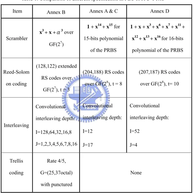
(10) List of Tables. Table 1: Comparison of different specification in FEC of ITU-T J.83 ......................................3 Table 2: Summary of CHIP Implementation for J.83 FEC ......................................................49 Table 3: Gate Count for each module.......................................................................................51 Table 4: Comparisons between the proposed architecture and other people’s work................52. v.
(11) Chapter 1 Introduction. 1.1. Motivation In communication system, channel coding which uses various types of error correcting. algorithm and interleaving techniques is a key module to minimize the effect of channel noise during data transmission. They can be summarized as the following four parts in most systems: scrambler, Reed-Solomon (RS) coding, interleaving, and trellis coding. And different applications have specific parameters to achieve an optimum system. Due to the similarity in FEC sections, such as ITU-T J.83 [1], DVB-T [2], and Advanced Television Systems Committee (ATSC) Digital TV [3], etc, a multi-mode FEC design will cause a lower cost design and better system integrations. For the RS code, it is not easy to implement a decoder that meets different finite field definitions and generator polynomials. Thus, each application has its own dedicated hardware for RS decoding. Moreover, memory controller of interleaver is also difficult to generate proper addresses for multi-standard. Hence, an efficient algorithm and architecture for multi-mode design is an important issue and challenge to lower down the design cost.. 1.2. Introduction to the platform 1.
(12) In ITU-T J.83, DVB-T, and ATSC Digital TV, etc, there are some similarities in FEC sections. However, ITU-T J.83 has the most kinds of modes than the other standards. Besides, the FEC sections in DVB-T and ATSC Digital TV are also included in ITU-J.83. Hence, ITU-T J.83 is chosen as the simulation plat form.. ITU-T J.83 is the digital multi-program systems for television, sound and data services for cable network. There are four annexes (A, B, C, and D), which provide the specification of J.83, including the frame structure, channel coding, and the method of modulation. A comparison of FEC section in different annexes of ITU-T J.83 is listed in table 1. The FEC is based on a concatenated coding approach that produces high coding gain at the moderate complexity and overhead. For main modules, there are three modes in RS codes, various parameters in convolutional interleaving, three kinds of scrambler and one trellis coding.. The main purpose of each FEC module is summarized as follows: (1) Reed-Solomon coding-Provide block encoding and decoding to correct up t symbols within each RS block. It can slightly resist channel burst errors. (2) Interleaving-Evenly spread the symbols by disordering the data sequence. It can protect the transmitted data against channel burst errors from being sent to RS decoder. (3) Scrambler-Randomize the data to allow effective modulation and prevent high PAPR (Peak-to-Average Power Ratio) after IFFT (inverse fast Fourier transform for OFMD-based systems). High PAPR will lower down the system performance. Scrambler can prevent this situation from happening. (4) Trellis coding-It is also called convolutional coding. By using Viterbi decoding algorithm (maximum likelihood decoding on trellis), it has very good ability of error correction. However, it is sensitive to channel burst errors. Hence, convolutional codes usually collaborate with interleaver and RS codes. 2.
(13) The details of FEC algorithm, decoding architecture, and the result of chip implementation will be described in later chapters, respectively.. Table 1: Comparison of different specification in FEC of ITU-T J.83 Item. Annex B. x3 + x +α3 over Scrambler. 7. Annex A & C. Annex D. 1 + x14 + x15 for. 1 + x + x3 + x6 + x7 + x11 +. 15-bits polynomial. x12 + x13 + x16 for 16-bits. of the PRBS. polynomial of the PRBS. GF(2 ). (128,122) extended Reed-Solom RS codes over on coding. 7. (204,188) RS codes. (207,187) RS codes. over GF(28), t = 8. over GF(28), t= 10. GF(2 ), t = 3 Convolutional. Convolutional. Convolutional. interleaving depth:. interleaving depth:. interleaving depth:. I=128,64,32,16,8. I=12. I=52. J=1,2,3,4,5,6,7,8,16. J=17. J=4. Interleaving. Trellis. Rate 4/5,. coding. G=(25,37octal). None. with punctured. 1.3. Thesis Organization The organization of this thesis is as follows. In chapter 2, the algorithm of FEC will be. described, including the algorithm of FEC encoder and decoder. It contains scrambler, 3.
(14) interleaver, Reed-Solomon codes and convolutional codes. And, the proposed algorithms and architectures of FEC for multi-standard will be addressed in chapter 3, which mainly contains a multi-mode RS decoder with memories to store and correct the received data and a memory-based universal convolutional interleaver and de-interleaver with a simple address generator. Chapter 4 will show the result of the chip implementation, the simulation result and will do some comparisons between other reference works and the proposed result. The last chapter is the conclusion and the future work.. 4.
(15) Chapter 2 Algorithm of FEC First of all, the encoder and decoder of FEC will be introduced. In ITU-T J.83, it can be divided into two main parts and composed of three or four processing layers. The first one is shown in figure 2.1(a), including ITU-T J.83 annex A, C, and D. The other is shown in figure 2.1(b), including ITU - T J.83 annex B. The following sections will define and introduce the algorithm of each layer in FEC.. in Scrambler. RS Encoder. Interleaver. to modulation. (a). in RS Encoder. Scrambler. Interleaver. Trellis Encoder. to modulation. (b) Figure 2.1: (a) FEC in ITU-T J.83 annexes A, C and D. (b) FEC in ITU-T J.83 annex B. 2.1. Scrambler 5.
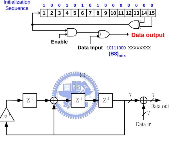
(16) The basic idea of scrambler is to randomize the transmitted data to provide the even distribution of the symbols in the constellation and to ensure adequate binary transitions for clock recovery.. Initialization Sequence. 1. 0. 0. 1. 0. 1. 0. 1. 0. 0. 0. 0. 0. 0. 0. 1 2 3 4 5 6 7 8 9 10 11 12 13 14 15. Data output Enable Data Input 10111000 XXXXXXXX (B8)HEX. (a). Z-1. Z-1. Z-1. 7. 7 Data out 7. α3. Data in. (b). D0. D1. D2. D3. D4. D5. D6. D7. (c) Figure 2.2: Scrambler in (a) J.83A, C and DVB-T system. (b) J.83B. (c) J.83D 6.
(17) Figure 2.2(a) shows the scrambler in J.83 annexes A, C and DVB-T systems. The scrambler adds a Pseudorandom Noise (PN) sequence to input symbols. And, the polynomial for the Pseudo-Random Binary Sequence (PRBS) generator is:. x15 + x 14 + 1. (2.1). At the start of every eight transport packets, the PRBS registers shall be initiated to the sequence “100101010000000”.. Figure 2.2(b) shows the scrambler in J.83B. The scrambler adds a PN sequence of 7-bit symbols over GF(128) to the input symbols to assure a random transmitted sequence. Initialization is defined as pre-loading to the “all one” state. The scrambler uses a linear feedback shift register specified by a GF(128) polynomial defined as follows: f ( x) = x 3 + x + α 3. (2.2). α 7 + α 3 +1 = 0. (2.3). Where:. The scrambler generator polynomial and initialization in J.83D are shown in figure 2.2(c). The PRBS is generated in a 16-bit shift register that has nine feedback taps. Eight of the shift registers outputs are selected as the fixed randomizing byte (D7 D6 D5 D4 D3 D2 D1 D0), where each bit from this byte is used to individually XOR the corresponding input data bit. The random generator polynomial is denoted as: x16 + x13 + x12 + x11 + x 7 + x 6 + x 3 + x + 1. (2.4). Where initialization is defined as pre-load to F180h, indicating the registers of x16, x15, x14, x13, x9 and x8 will be loaded to 1 during the field sync interval.. The structure of de-scrambler is the same as scrambler since PRBS generator is 7.
(18) constructed by shift registers and all operations are XORS.. 2.2. Interleaving The main purpose of interleaving is to resist burst errors, which are induced in noisy. channel. It rearranges the order of input data sequence. Generally, there are two kinds of techniques of interleaving. One is block interleaving, and the other is convolutional interleaving. However, convolutional interleaving has better ability to spread burst errors than block interleaving.. The structure of (I, J) convolutional interleaver and deinterleaver based on Forney approach [8] and Ramsey type III approach [5] is shown in figure 2.3. The parameter I is the interleaving depth and is chosen to be larger than the maximum expected length of burst errors. It also represents that there are I branches in the structure of convolutional interleaving. The parameter J is usually chosen such that I x J should be larger than the decoding constraint length for convolutional codes. It also means that branch 0 has zero delays in convolutional interleaver. And, there are J shift registers in branch 1, 2J shift registers in branch 2, and son on, (I-1) x J shift registers in branch I-1. Convolutional de-interleaver has the inverse of this property. Hence, the memory requirement is J x I x (I-1) / 2 in both convolutional interleaver and deinterleaver. The total end-to-end delay is J x I x (I-1). This is half the required delay and memory in the block interleaving.. The operation of convolutional interleaving is that at the start of the FEC frame, the input switch is initialized to the top-most branch. Then, the input switch is cyclically connected to the other branches as the valid symbols come in. So does the output switch. And, the input and output switches shall be synchronized. 8.
(19) Interleaver. De-Interleaver. 0. J J. 2. J. J. J. .... 1 symbol per position I-1. .... 1. J. 0. J ... J. J. I-3. J. I-2. J ... J. I-1. Figure 2.3: Structure of (I, J) convolutional interleaving. Taking (12, 17) convolutional interleaver for an example, this interleaver is adopted in J.83 annexes A, C and DVB-T systems. Assume the input sequence is 0, 1, 2, …, 204, 205, …, and so on. Where the number means the input timing index. And the output sequence will be 0, x, x, …, x, 12, x, x, …, x, 204, 1, x x, …, x, 2244, 2041, …, 11, and so on, as shown in figure 2.4. Where x means “the don’t care symbols” at the beginning transmission. Hence, the burst errors will be spread out as the pseudo noise after deinterleaving. And, the data should be reordered to the original sequence after deinterleaving in receiver part.. 2244. 2040. 2041. 1837. 1838. 1634. ... 406 . . . 226 214 202 . . . 22 203 . . . 23. 11. 10. X ... X X. 600 . . . 420 408 396 . . . 216 204 192 . . . 12. .... 397 . . . 217 205 193 . . . 13 194 . . . 14. ... X . . ... .. 2. X ... X X X . . . . . . . . . . . .. ... ... . . .. 1. X X X X . . . . . .. X ... X ... . . . . . . . .. 0. X X X . . . .. X . . . .. Figure 2.4: The output symbols in convolutional interleaver with I = 12, J = 17. In J.83 annexes A, C, DVB-T and ATSC Digital TV system, the convolutional interleaving is with I = 12 and J = 17. In J.83 annex D, the convolutional interleaving is with I = 52 and J = 4. The upper systems have only one dedicated parameters. However, the convolutional interleaving in J.83 annex B has lots of different modes to be operated. That is, 9.
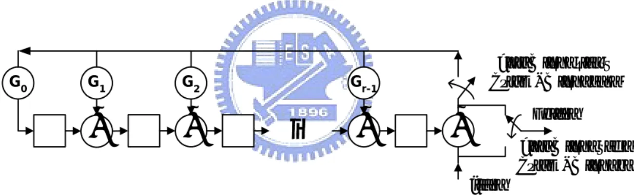
(20) I can be 128, 64, 32, 16 and 8. J can be 1, 2, 3 ~ 7, 8 and 16. The most critical mode is with I = 128, J = 8. The detail information about specifications is in [1].. 2.3. Reed-Solomon Codes Reed-Solomon codes have become the most important code of various types of. error-control codes due to its superior capability for burst error correcting and the feasibility for digital implementation. Hence, RS codes are widely adopted in many data communication applications, such as digital TV system, compact disk (CD), and digital versatile disk (DVD). It is adopted in DVB-T, ITU-J.83 cable systems, too. A (N, K) RS codes over GF(2m) contain N coded symbols with K message symbols and can correct up to t = ⎣ N-K / 2 ⎦ errors. Note that each symbol over GF(2m) has m bits and all operations in RS codes are based on GF(2m) [11][12].. 2.3.1. Reed-Solomon encoder. Let (MK-1, MK-2, …, M1, M0) denote K message symbols that are to be transmitted. So the message polynomial: M ( x) = M K −1 x K −1 + M K −2 x K −2 +. + M1x + M 0. (2.5). And, there is a generator polynomial: g ( x) = ( x + α h )( x + α h+1 ). ( x + α h+ 2t −1 ). (2.6). Where g(x) has the degree of 2t, h may be 0 or 1, and α is the primitive n-th root over GF(2m). Firstly, the message polynomial M(x) is multiplied by x2t and then divided by the generator polynomial g(x) to obtain a remainder polynomial R(x):. 10.
(21) M ( x) x 2t = q ( x) g ( x) + R ( x) R ( x) = R2t −1 x 2t −1 + R2t −2 x 2t − 2 +. (2.7). + R1 x + R0. (2.8). Then, the codeword polynomial C(x) with the systematic form can be expressed as: C ( x) = q( x) g ( x) = M ( x) x 2t + R ( x) = M K −1 x 2t + K −1 +. + M 0 x 2t + R2t −1 x 2t −1 + … + R1 x + R0. (2.9). The previous description of RS encoder can be implemented as the systematic feedback shift register encoder as shown in figure 2.5 [11][12], where G0, G1, …, Gr-1 is the coefficient of the generator polynomial. In first K cycles, it will output the message M(x). In last N-K cycles, it will output R(x). This forms the final codeword C(x).. G0. G1. +. +. First K ticks closed Last N - K ticks open. Gr-1. G2. …. Output. +. +. First K ticks down Last N - K ticks up. Input. Figure 2.5: The circuit of the systematic feedback shift register RS encoder. For J.83 annex A and C, the (204, 188) RS codes over GF(28) are utilized for correcting 8 errors. The code generator polynomial is denoted as: g ( x) = ( x + α 0 )( x + α 1 ). ( x + α 15 ). (2.10). Where α represents the primitive element for the primitive polynomial: p ( x) = x 8 + x 4 + x 3 + x 2 + 1. 11. (2.11).
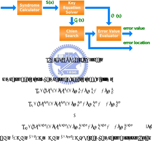
(22) For J.83 annex B, the RS encoder is utilized to implement a t = 3, (128, 122) extended RS codes over GF(27). The primitive polynomial used to form the filed over GF(27) is: p ( x) = x 7 + x 3 + 1. (2.12). And the generator polynomial is: g ( x) = ( x + α 1 )( x + α 2 ). (x + α 5 ). (2.13). After C(x) is generated from equation (2.9), an extended parity symbol C_ is generated by evaluating the codeword at the sixth power of α and denoted as C_ = C(α6). This extended symbol is used to form the last symbol of a transmitted RS codeword. The extended codeword polynomial Cˆ ( x) is then as follows: Cˆ ( x) = xC ( x) + C _ = M 121 x127 +. + M 0 x 6 + R4 x 5 + R0 x + C _. (2.14). (207, 187) RS codes with t = 10 over GF(28) are utilized for J.83 annex D. The generator polynomial g(x) is shown as follows: g ( x) = ( x + α 0 )( x + α 1 ). 2.3.2. ( x + α 19 ). (2.15). Reed-Solomon decoder. Assume the received data polynomial is r(x), and error polynomial is e(x). That is: r ( x ) = c ( x ) + e( x ). (2.16). And, e( x) = e1 X 1 + e2 X 2 +. + ev X v ,0 ≤ v ≤ t. (2.17). Where ei is the error value, Xi is the error location, and v is the error numbers. And, Reed-Solomon decoding process can be divided into four steps [4]: (1) syndrome calculator, (2) Key equation solver, (3) chien Search, and (4) error value evaluator, as shown in figure 2.6. 12.
(23) The syndrome calculator calculates a set of syndromes from the received codewords. The key equation solver produces the error locator polynomial σ (x) and the error value evaluator polynomial Ω(x) from the syndromes. By the chien search and the error value evaluator, we can get the error locations and error values respectively.. Syndrome Calculator. S(x). Key Equation Solver. Ω (x). σ (x) Chien Search. Error Value Evaluator. error value. error location. Figure 2.6: RS decoding process. In syndrome calculator, the syndromes are calculated as follows: S1 = r (α h ) = e(α h ) = e1 Χ1h + e2 Χ 2h + S 2 = r (α h+1 ) = e(α h+1 ) = e1Χ1h+1 + e2 Χ h2+1 +. + ev Χ vh + ev Χ vh+1. S 2t = r (α h+ 2t −1 ) = e(α h+ 2t −1 ) = e1 Χ1h+ 2t −1 + e2 Χ 2h+ 2t −1 +. + ev Χ vh+ 2t −1. (2.18). Since C(αh) = C(αh + 1) = … = C(αh + 2t - 1) = 0. Hence, the syndrome polynomial can be defined as:. 13.
(24) S ( x) = S1 + S 2 x +. + S 2t x 2t −1. = e1 Χ1h (1 + Χ1 x + Χ12 x 2 +. + X 12t −1 x 2t −1 ). + e2 Χ 2h (1 + Χ 2 x + Χ 22 x 2 +. + X 22t −1 x 2t −1 ). + ev Χ vh (1 + Χ v x + Χ v2 x 2 +. + X v2t −1 x 2t −1 ). e1 Χ1h (1 − ( Χ1 x) 2t ) e2 Χ 2h (1 − ( Χ 2 x) 2t ) = + + 1 − Χ1 x 1− Χ2 x. ev Χ vh (1 − ( Χ v x) 2t ) + 1− Χv x. (2.19). The equation (2.19) will be used later for calculating the error values ei, 0 ≤ I ≤ t.. For the extended RS codes in J.83B, the syndrome should be modified. Recall r(x) = Cˆ ( x) + e( x) = xC ( x) + C __ + e( x) ; there are two cases discussed individually as follows: (1) r0 is not an error, meaning r0 = C_. The decoding procedure is the same as the normal cases. (2) r0 is an error, meaning r0 = C_+e_. Then, S1 = r (α h ) = e(α h ) = e1 Χ 1h + e2 Χ 2h +. + ev Χ vh + e _. S 2 = r (α h +1 ) = e(α h +1 ) = e1 Χ 1h +1 + e2 Χ 2h +1 +. S 2t = r (α h + 2t −1 ) = e(α h + 2t −1 ) = e1 Χ 1h + 2t −1 + e2 Χ h2 + 2t −1 +. + ev Χ vh +1 + e _. + ev Χ vh + 2t −1 + e _. (2.20). While v ≤ t , the error value e_ can be calculated to let the discrepancy ∆( 2t −1) = 0 during solving key equation by Berlekamp-Massey algorithm that will be introduced later.. The key equation is defined as follows:. Ω( x) = S ( x)σ ( x) mod x 2t. (2.21). Where Ω( x) is the error evaluator polynomial, and σ ( x ) is the error locator polynomial. 14.
(25) The key equation can be solved by Euclidean algorithm or Berlekamp-Massey (BM) algorithm [11][12][19].. An inversionless BM algorithm which is a 2t-step iterative algorithm is shown as follows [4]: Initial condition:. D ( −1) = 0; δ = 1; σ ( −1) ( x) = τ ( −1) ( x) = 1; ∆( 0 ) = S1. (2.22). For (i = 0 to 2t-1). ⎧⎪σ ( i ) ( x) = δ ⋅ σ (i−1) ( x) + ∆( i ) xτ ( i−1) ( x) ⎨ (i +1) (i ) (i ) (i ) ⎪⎩∆ = Si +2 ⋅ σ 0 + Si +1σ 1 + + Si +2−tσ t. (2.23). If ( ∆(i ) = 0 or 2 D (i −1) ≥ i + 1 ). D ( i ) = D ( i −1) , τ ( i ) ( x) = xτ ( i −1) ( x). (2.24). D ( i ) = i + 1 − D (i −1) , δ = ∆( i ) , τ ( i ) ( x) = σ ( i −1) ( x). (2.25). else. Where σ (i ) ( x) is the i-th step error locator polynomial and σ (ij ) is the coefficient of. σ (i ) ( x) . ∆(i ) is the i-th step discrepancy and δ is the previous discrepancy. τ (i ) ( x) is an assisting polynomial and D (i ) is an assisting degree variable in i-th step.. And the modified inversionless BM algorithm with some differences in initial conditions can be shown as follows [4]:. σ. (i ) j. ⎧⎪δ ⋅ σ 0(i −1) , =⎨ ( i −1) ( i ) ( i −1) ⎪⎩δ ⋅ σ j + ∆ τ j −1 ,. ⎧0, ∆(ij+1) = ⎨ ( i +1) (i ) ⎩∆ j −1 + S i − j +3 ⋅ σ j −1 ,. for j = 0 for 1 ≤ j ≤ t. for j = 0 for 1 ≤ j ≤ t. (2.26). (2.27). Where τ (ij ) is the coefficient of τ ( i ) ( x) and ∆(ij ) is the partial results in computing ∆(i ) . 15.
(26) Besides, if σ(x) is first obtained, from the key equation and the Newton’s identity we could derive Ω( x) as follows:. ⎧⎪S ⋅ σ , Ω (ji ) = ⎨ i +( i1) 0 ⎪⎩Ω j −1 + S i − j +1 ⋅ σ j ,. for j = 0 for 1 ≤ j ≤ i. (2.28). These modified inversionless BM equation will be adopted in our proposed multi-mode key equation solver because of its regularity.. The alternative algorithm of key equation solver is Euclidean algorithm. It can be summarized as follows: Initial condition:. ⎧σ −1 ( x) = 0, σ 0 ( x) = 1 ⎨ −1 2t 0 ⎩Ω ( x) = x , Ω ( x) = S ( x). (2.29). Do the following operation until deg{ σ ( x ) } > deg{ Ω( x) }:. ⎧σ i ( x) = σ i−2 ( x) + q i −1 ( x)σ i −1 ( x) ⎨ i i −2 i −1 i −1 ⎩Ω ( x) = Ω ( x) + q ( x)Ω ( x). (2.30). Where σ i ( x) is the i-th step error locator polynomial, Ω i ( x) is the i-th step error evaluator polynomial, and qi(x) is the i-th quotient polynomial generated in key equation.. After solving the key equation, we find the roots of σ ( x) for error location X1, X2, …, Xv in chien search, where the roots of σ ( x) are X 1−1 , X 2−1 ,. , X v−1 . Hence, σ ( x) can be. represented as:. σ ( x) = (1 − X 1 x)(1 − X 2 x) (1 − X v x). (2.31). Then, using Forney algorithm to calculate error values in error value evaluator and together key equation and equation (2.19), we can get: 16.
(27) Ω( x) = S ( x)σ ( x) mod x 2t = e1 Χ1h (1 − Χ 2 x)(1 − Χ 3 x). (1 − Χ v x). + e2 Χ h2 (1 − Χ1 x)(1 − Χ 3 x). (1 − Χ v x). + ev Χ vh (1 − Χ1 x)(1 − Χ 2 x). (1 − Χ v −1 x). (2.32). And, the former derivative of σ (x) can be represented as: dσ ( x ) = Χ1 (1 − Χ 2 x)(1 − Χ 3 x) (1 − Χ v x) dx + Χ 2 (1 − Χ1 x)(1 − Χ 3 x) (1 − Χ v x). + Χ v (1 − Χ1 x)(1 − Χ 2 x). =. (1 − Χ v −1 x). σ odd ( x). (2.33). x. Where σ odd (x) is the odd parts of σ (x) . Hence, combine the equations (2.32) and (2.33), the error values can be calculated as follows: ei =. Ω( X i−1 ) σ ′( X i−1 ) X ih−1. (2.34). Where σ ′(x) is the formal derivative of σ (x) over GF(2m).. According to the error locations and error values solved from previous algorithm, we can correct the channel induced errors in received data and get the correct codeword. Unfortunately, if error numbers in one codeword are larger than t, we could not correct the received data.. For more information about RS decoding process, please see [4] [11][12][19].. 17.
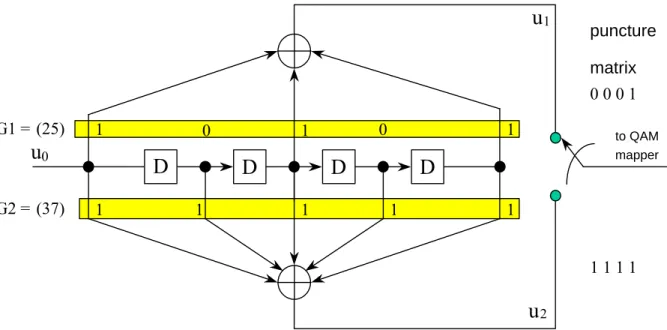
(28) 2.4. Trellis Codes In a (n, k, m) Trellis code (or called convolutional code), the coded n-bit output block. depends not only on the corresponding k-bit input message block, but also on the m previous message blocks. It can be implemented with an n-output, k-input linear sequential circuit with an input memory of m words. The advantage of the convolutional codes is that it allows the introduction of redundancy to improve the threshold Signal-to-Noise Ratio.. Only J.83 annex B contains the trellis code. This trellis-coded modulator is a 16-state non-systematic rate 1/2 encoder with the generator: (G1, G2) = (25, 37octal) The punctured matrix proposed in [13] essentially converts the rate 1/2 encoder to rate 5/4. The punctured matrix is defined as: (P1, P2) = (0001, 1111). The internal structure of the punctured convolutional encoder is illustrated in figure 2.7.. 18.
(29) u1. puncture matrix 0001. G1 = (25). 1. u0 G2 = (37). 0. D 1. 0. 1. D 1. 1. D 1. to QAM mapper. D 1. 1 1111. u2 Figure 2.7: Punctured binary convolutional codes in ITU-T J.83B. The Viterbi algorithm proposed in 1967 is a straightforward implementation of the maximum likelihood (ML) decoder and is the most powerful and popular algorithm for decoding convolutional codes [14][15]. The following four steps are Viterbi algorithm, which can be applied to find the ML path: (1) According to the current received input datum, we calculate the transition metrics (TM) to the next transition states. (2) Sum the previous path metrics (PM) with the calculated TM and compare tow paths, which come from different states but merge at the same current state. Then, we select the path with the smallest distance. This operation is called ACS (Add-Compare-Select), and we use ACS unit for each state. (3) The output of the select branch in each state is stored into the memory, which is called “survivor path”. (4) Repeat (1), (2) and (3) until the memory of survivor path is full, then the output decision begins to trace-back the survivor path to find the output of the smallest path metrics (the 19.
(30) ML path).. In practice, the register-exchange approach and trace-back approach are useful methods for survivor path storage management in Viterbi decoder architecture. The former one takes more area but less time than the latter one. We will use register-exchange method to implement the survivor path storage management in Viterbi decoder since the convolutional codes in J.83B has only 16 states and thus the number of registers required for this decoder is not quite large. The detail architecture of Viterbi decoder for J.83B will be introduced in chapter 3.4.2.. 2.5. Summary In this chapter, we introduce the encoding and decoding algorithm of each FEC section.. It includes scrambler, interleaving, RS codes and convolutional codes. In chapter 2.1, three kinds of scrambler of J.83 are introduced. In chapter 2.2, both convolutional interleaver and deinterleaver are introduced. It has more advantage than block interleaving. In chapter 2.3, the encoding and decoding algorithm of RS codes is introduced. In RS decoding algorithm, two kinds of key equation solver are presented. One is BM algorithm, and the other is Euclidean algorithm. We also introduce three kinds of RS codes among J.83, one is over GF(27) with t = 3, the others are in GF(28) with t = 8 and 10, respectively. In chapter 2.4, we introduce the convolutional codes and Viterbi algorithm. Fortunately, it has only one mode in J.83, that is, a 16-state non-systematic rate 1/2 encoder with the generator: (G1, G2) = (25, 37octal).. 20.
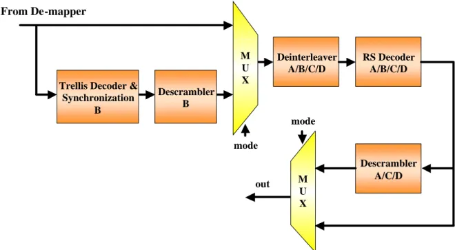
(31) Chapter 3 Algorithm and Architecture for Multi Mode FEC Decoder. The algorithm and architecture of a multi-mode RS decoder with memories to store and correct the received data and a memory-based universal convolutional interleaver/ de-interleaver will be proposed in this chapter. These two modules are compatible for ITU-T J.83, DVB-T, ATSC Digital TV systems, etc. The scrambler and Viterbi decoder will be only mentioned briefly since the complexity of scrambler is so simple and there is only one kind of convolutional codes.. 3.1. The proposed multi-mode FEC decoder Figure 3.1 shows the block diagram of the proposed multi-mode FEC decoder. It. integrates all systems from figure 2.1 into one system. The symbols A/B/C/D represent the annex A/B/C/D in ITU-T J.83. The different data paths between J.83 annex B and annex A/C/D are decided by multiplexer.. 21.
(32) From De-mapper. Trellis Decoder & Synchronization B. M U X. Deinterleaver A/B/C/D. RS Decoder A/B/C/D. Descrambler B mode mode. out. M U X. Descrambler A/C/D. Figure 3.1: The proposed multi-mode FEC decoder. 3.2. Memory-based universal convolutional interleaver/ de-interleaver It is not efficient for implementing so many pieces of FIFO in convolutional interleaver. or deinterleaver since it consumes lots of power, area and induces routing difficulty in APR (Auto Placement and Route). Hence, a better solution is to use SRAM to solve these problems. The key issue becomes how to generate the correct address of SRAM for each input and output data. As a result, a novel, low complexity, high flexibility and memory-based method to implement the multi-mode convolutional interleaver and deinterleaver is proposed, which is induced from [6][7].. 22.
(33) 3.2.1. The algorithm and architecture of memory-based universal convolutional. interleaving The idea is that we rebuilt the FIFO registers of convolutional deinterleaver as a memory array. Assume the FIFO registers in first branch are put in somewhere of the memory array, and the FIFO registers in second branch are appended latter, and so on, until the last FIFO registers are appended. Hence, the memory array is as shown in figure 3.2. For writing, we realize that after writing first symbol into the head of the memory array, the next symbol should be written into the head of the second branch, i.e., the address distance of memory between first symbol and second symbol is (I-1) x J. The values are the same as the numbers of the FIFO in first branch. Hence, we call this “branch address”. And the address for first symbol is called intra-initial address. For the third symbol, the address distance of memory between second symbol and third symbol is (I-2) x J. And so on, the address distance of memory between (I-2)-th symbol and (I-1)-th symbol is 2J. In contrast to write, the first readout symbol should be in the end of the first branch in memory array. The second readout symbol should be in the end of the second branch, i.e., the address distance between first symbol and second symbol is (I-2) x J. Similarly, the address distance between second symbol and third symbol is (I-3) x J. And so on, the address distance between (I-2)-th symbol and (I-1)-th symbol is J. For the coincidence of writing and reading direction, the initial address pointer should be decreased by 1 for the next I symbols. Then, do the previous operation again. In addition, the memory size should be defined. If the memory address is out of the memory size, it should modulo the address by the memory size.. 23.
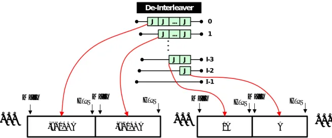
(34) De-Interleaver J. .... J. 0. J. .... J. 1. J. I-3. .... J. J. J. I-2 I-1. Write. .... Read. (I - 1) * J. Write. Write. Read. .... (I - 2) * J. Read. 2J. Write. Read. J. .... Figure 3.2: The memory array by rebuilding the FIFO registers of deinterleaver. A (12, 17) convolutional deinterleaver which is adopted in ITU-T J.83A, C and DVB-T system will be taken for an example to show how it works. Assume the datum we received are 0, x, x, …, x, 12, x, x, …, x, 204, 1, x, x, …, x, 2244, 2041, …, 11, …, as shown in figure 2.4. Where the number means the input indexes from interleaver, and x means “don’t care symbols” at the beginning. When deinterleaving, after writing 0 to memory, the interval between 0 and the next writing address is (I-1) x J = 187 as shown in figure 3.3(a). The interval between previous address and the next address is (I-2) x J = 170, and so on, until to 2J = 34. These numbers are the same as the numbers of FIFO on branches of convolutional deinterleaver. When writing 12 to the memory, it needs go back to the address of “initial writing address-1” and does the previous operation again. After writing 202 into the memory, the data stored in memory is like in figure 3.3(b). Then we can see that the distance between 0 and 1 is (I-2) x J = 170. The distance between 1 and 2 is (I-3) x J = 153, and so on. The distance between 9 and 10 is J = 17. At this time, the memory size in figure 3.3(b) is J x I x (I-1) / 2, just the same as the minimum memory requirement in figure 2.3. Because there is no more space to write 2244 into memory, so it must increase more memory sizes. Or it will violate the rules. By the observation, it needs more J memory size. As shown in figure 3.3(c), 24.
(35) when 0 is read out from memory, 2244 is written into memory. And, 1 is read out, 2041 is written to the original position of 0. Then, do the previous operation again. In addition, when the address is out of the memory size, it must modulo the address by the memory size. Hence, the required memory size is J x I x (I-1) / 2 + J. The maximum size is 65032 bytes for (128, 8) convolutional deinterleaver in J.83B. We realize that it just needs more 8 bytes than the original structure and has the advantage of low cost and high flexibility for multi-mode design.. (I-2)xJ 170. (I-1)xJ 187 204. .... ... 24 12 0. 1. X. X. X. .... X. 187 (a). (I-1)xJ 187 2232 2220 2208. (I-2)xJ 170. .... 36 24 12 0. 2029 2017 2005. .... J 17 25 13 1. .... .... 9 202. 22 10. (b). 187 2244 2232 2220. .... 170 12 0. 2029 2017. .... 17 13 1. .... 9 202. .... 22 10. (c) Figure 3.3: Behavior of the novel algorithm for (12, 17) convolutional deinterleaver. 25.
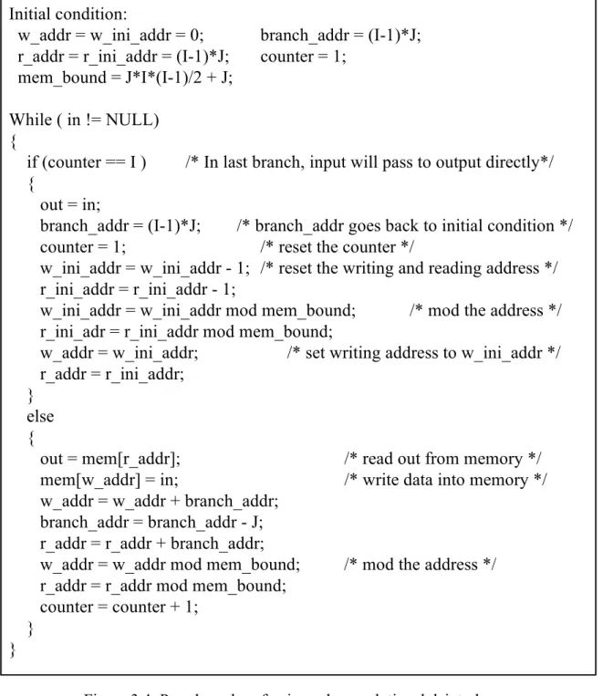
(36) The detail operations of universal convolutional deinterleaver are described as pseudo codes in figure 3.4, where there are 12 parameters that we used: (1) I: Interleaver depth (2) J: The difference delays between each neighboring branch (3) in: data input. (4) out: data output. (5) w_addr: The writing address for memory input. (6) r_addr: The reading address from memory to output (7) w_ini_addr: The intra-initial address of w_addr. (8) r_ini_addr: The intra-initial address of r_addr. (9) branch_addr: This is the address between 2 neighboring data. (10) counter: For determining when to output directly and reset w_addr and r_addr. (11) mem_bound: Maximum size of memory (12) mem[ ]: It represent the memory and the size is mem_bound.. Convolutional interleaver which is the inverse of convolutional deinterleaver can be easily formulated, too.. 26.
(37) Initial condition: w_addr = w_ini_addr = 0; r_addr = r_ini_addr = (I-1)*J; mem_bound = J*I*(I-1)/2 + J;. branch_addr = (I-1)*J; counter = 1;. While ( in != NULL) { if (counter == I ) /* In last branch, input will pass to output directly*/ { out = in; branch_addr = (I-1)*J; /* branch_addr goes back to initial condition */ counter = 1; /* reset the counter */ w_ini_addr = w_ini_addr - 1; /* reset the writing and reading address */ r_ini_addr = r_ini_addr - 1; w_ini_addr = w_ini_addr mod mem_bound; /* mod the address */ r_ini_adr = r_ini_addr mod mem_bound; w_addr = w_ini_addr; /* set writing address to w_ini_addr */ r_addr = r_ini_addr; } else { out = mem[r_addr]; /* read out from memory */ mem[w_addr] = in; /* write data into memory */ w_addr = w_addr + branch_addr; branch_addr = branch_addr - J; r_addr = r_addr + branch_addr; w_addr = w_addr mod mem_bound; /* mod the address */ r_addr = r_addr mod mem_bound; counter = counter + 1; } } Figure 3.4: Pseudo codes of universal convolutional deinterleaver. The architecture of the proposed algorithm for convolutional interleaving is depicted in figure 3.5. FSM controls the branch address generator and the intra-initial address generator. Combining the branch address and intra-initial address together forms the final address for memory.. 27.
(38) Read intra-initial address. M U X. D FF. mod Read branch address. Final read address. FSM. SRAM Final write address. Write branch address mod. Write intra-initial address. M U X. D FF. Figure 3.5: The architecture of the address generator for convolutional interleaving. 3.3. The multi-mode RS decoder To design a multi-mode RS decoder, at first, a finite field multiplier (FFM) for different. finite field definition should be designed. Then, the four steps of RS decoding process [4] can be proceeded. As a result, in the sub-section, the multi-mode FFM will be proposed in the first. Then, the multi-mode syndrome calculator, key equation solver, chien search and error value evaluator will be proposed, respectively. The multi-mode RS decoder can be used in many applications, such as ITU-T J.83, DVB-T systems, etc.. 28.
(39) 3.3.1. Multi-Mode Finite Field Multiplier. For different RS codes, the different primitive polynomial will cause a challenge to design a FFM. However, FFM can be split into multiply and modular operation respectively. The primitive polynomial only has an impact on modular operation. Therefore, the complexity of programmable design just lies in the modular operation. So, a multi-mode FFM is proposed as shown in figure 3.6, where pi(x) and pj(x) are different primitive polynomial over GF(2m) respectively.. mode A. mod(pj(x)). B. mux. Multiplier. mod(pi(x)) C. . . .. Figure 3.6: Multi-mode FFM over GF(2m). 3.3.2. Syndrome Calculator. To calculate the syndromes, we can use Horner’s Rule: u ( x) = u n x n + u n−1 x n−1 +. + u1 x + u 0. = ( (((u n x + u n−1 ) x + u n−2 ) x + u n−3 ) ) x + u 0. 29. (3.1).
(40) × α 8i. × α 8i × α 7i. mux. Rj. mode. +. Si. +. Rj. SCi. SC2 i (b). (a). SC0. Si. SC2 1. SC2 2. SC2 3. SC2 4. i SC2 5. SC2 6. SC7. SC 8. SC9. Rj SC 10. SC11. SC 12. SC13. SC 14. SC 15. SC16. SC 17. SC18. SC 19. 20×8 Registers. mode. Si. (c) Figure 3.7: Multi-mode syndrome calculator: (a) Basic cell SCi for GF(28). (b) Basic cell SC2i for dual mode purpose (GF(28) and GF(27)). (c) The overall structure of multi-mode syndrome calculator. Hence, the basic cell to calculate the syndrome based on Horner’s Rule should be proposed at first. In the simulation platform of J.83, there are two kinds of finite field, the one is GF(28), the other is GF(27). Besides, the roots of the generator polynomial are from α0 to α2t-1 in J.83A, C and D. But in J.83B, the roots of the generator polynomial are from α1 to α2t-1. Hence, the two kinds of different basic cells SCi and SC2i are proposed as shown in. figure 3.7(a)and (b). SCi is for GF(28); SC2i is for GF(28) and GF(27) which are decided by 30.
(41) the current mode. The architecture of multi-mode syndrome calculator is shown in figure 3.7(c). For different specification, a specific group of cells will be chosen. For J.83 A and C, SC0, SC1, …, SC15 will be chosen. SC21, SC22,…, SC26 will be chosen in J.83B. All basic cells will be chosen for J.83D.. Based on [9], moreover, the first t syndromes are equal to zeros implies all syndromes are zeros, which can simplify the error detection procedure. It not only improves the power consumption, but also reduces the complexity.. 3.3.3. Key Equation Solver. To solve the key equation, Berlekamp-Massey algorithm is used due to its regular operation. For different t, it needs 2t iterations to find error locator polynomial σ(x). Base on the proposed multi-mode FFM and modified decomposed algorithm [4][9] mentioned in chapter 2.3.2, the architecture of multi-mode key equation solver is proposed as shown in figure 3.8. The computation of Ω(x) after σ(x) results in fewer multiplications and additions than the original BM algorithm. It includes only one key equation solver with three proposed multi-mode FFMs to calculate σ(x) and Ω(x) respectively. Hence, the hardware complexity is reduced.. 31.
(42) σ(x). FFM. Si. +. ∆. δ. FFM. FFM. mux. τ(x). + Figure 3.8: Multi-mode key equation solver. 3.3.4. Chien Search. Similar to syndrome calculator, for the different finite field (GF(27) and GF(28)) and the capability of error correction t, the two kinds of basic cells Ci and C2i are proposed for multi-mode chien search as shown in figure 3.9(a) and (b). Ci is designed only for GF(28). C2i is designed for GF(28) and GF(27). And the architecture of multi-mode chien search is depicted in figure 3.9(c). For different specifications, the sums of proper cells will be chosen. The sums of C20, C21, C22 and C23 are chosen for J.83B. The sums of C20, C21, C22, C23, C4 , C5, …, C8 are chosen for J.83A and C. The sums of C20, C21, C22, C23, C4 , C5, …, C10 are chosen for J.83D. And the cell of C2L calculates the current calculating location. If the sums are equal to zero, the location will be stored in the registers.. 32.
(43) mode. × α 8− i. mux. × α 8− i × α 7− i. pi. mux. pi. mux. σj. σj. Ci. C2i. (a) mode. σ0. C20. (b). σ1. σ2. C21. σ3. C22. C23. σ9. σ10. C9. C10 mode. +. +. mux. +. =0 ? trap. C4. C5. C6. C7. C8. C2L. σ4. σ5. σ6. σ7. σ8. 1 mode. 10×8 Registers. (c) Figure 3.9: Multi-mode chien search. (a) Basic cell Ci for GF(28). (b) Basic cell C2i for dual mode purpose (GF(28) and GF(27)). (c) The overall structure of multi-mode chien search.. 3.3.5. Error Value Evaluator. Based on Forney algorithm and assume βj is the j-th root of error locator polynomial. For J.83A, C and D, the error value: ei =. Ω( β j ) β jσ ′( β j ). 33. (3.2).
(44) For J.83B, the error value: ei =. Ω( β j ) σ ′( β j ). (3.3). Based on the previous equations, the architecture of multi-mode error value evaluator is proposed as shown in figure 3.10. It will calculate σ’(βj) and Ω(βj) at the same time while the left multiplexer will choose βj2 , the bottom multiplexer will choose βj. After calculating σ’(βj), σ’(βj) will multiply βj for J.83A,C and D. The block of “( )-1” is implemented by a table. In order to calculate the final error value, the bottom multiplexer will choose the upper path.. mux. βj β j2 1. FFM ( )-1. βj. FFM. +. mux. σ 2k+1. + Ωk. Figure 3.10: Multi-mode error value evaluator. 3.3.6. Memory structure to correct the RS codeword. Based on the proposed architecture, the memory requirement is four times the codeword length because of the output latency. And, because of the output latency, memory structure is built as two interleaved structure to avoid accessing the same bank of memory in writing the current RS codeword and correcting the previous RS codeword at the same time, as shown in figure 3.11. The interleaved structure of memory is that packet 0 of RS codeword is written into bank 0 of memory, packet 1 is written into bank 1, packet 2 is written into bank 0, and 34.
(45) packet 3 is written into bank 1. Due to the output latency, we will know the error location and error value of RS codeword 0 until writing packet 3 into the memory. When correcting packet 1 in bank 1, the packet 4 is written into bank 0, and so on. Hence, it avoids accessing the same memory bank at the same time. Based on this interleaved structure of memory, the memory requirement for multi-mode RS decoder is 752 bytes (two 188x2 bytes) since the maximum K is 188.. Begin to Correcting read out Time for packet 1 Packet 1. Bank 0 Bank 1. Packet 0. Packet 0. Packet 4. Packet 2. Packet 2. Packet 2. Packet 1. Packet 1. Packet 1. Packet 3. Packet 3. Packet 3. Correcting Time for Packet 0. Begin to read out packet 0. Figure 3.11: The operation of accessing memory in multi-mode RS decoder. 3.4. Other Components. 3.4.1. De-scrambler. The circuit complexity of scrambler is so simple that it is suggested to use dedicated hardware for different annexes. Because of the property of “serial in serial out” in J.83A and C, we can transform the structure of scrambler into the one as shown in figure 3.12. The 35.
(46) transformed structure has the property of “symbol in symbol out”. Hence, the serial to parallel converter or parallel to serial converter can be omitted. The other annexes can be implemented as the original structure.. Every cycle, it shifts 8 bits 1. Initialization Sequence. 2. 3. 4. 5. 6. 7. 8. 9 10 11 12 13 14 15. 1 0 0 1 0 1 0 1 0 0 0 0 0 0 0. 8 bits 8 bits. 8 bits. Data output Enable Data Input. (B8) XXXXXXXX HEX. Figure 3.12: The transformed structure of scrambler in J.83A and C. 3.4.2. Viterbi Decoder. Trellis coding is only included in J.83B. Using hard-decision Viterbi decoder with 16 states can fit the requirement of ITU-T J.83B.. We take register-exchange method as the architecture of survivor path storage management to realize the Trellis decoder since the convolutional codes in J.83B has only 16 states and thus the number of registers required for this decoder is not quite large. According to this approach, we assign one register to each state. Each register records the decoded output sequence along the survivor path for each state, as shown in figure 3.13 [16]. The decoded output sequence stored in survival memory (SM) depends on the path of minimum sum of the 36.
(47) coming TM and the previous PM. At the last stage, we select the sequence content stored in the register of the state with minimum PM.. S0. 0. 00. 100. 1000. 10000. 100000. S1. 1. 01. 101. 0101. 11101. 101101. ………………… S2. 0. 10. 010. 1110. 10110. 010110. S3. 1. 11. 111. 1011. 01011. 111011. T=1. T=2. T=3. T=4. T=5. T=6. T=0. Figure 3.13: Register contents for register-exchange method. S0. S0 MUX. S0 MUX. REG. REG. S1. S1 MUX. REG. S2 MUX. REG S2. S3. (a). (b). Figure 3.14: Architecture of register-exchange approach applied in SM unit. (a) Trellis diagram. (b) The connections of registers and multiplexers between each state.. The implementation of register-exchange method is really simple. The connections of registers and multiplexers between each state are decided by Trellis diagram. Using the property of the structure of trellis diagram as shown in figure 3.14(a), it is shown that there are always two states having the same previous two states. And, the current SM will select the 37.
(48) minimum path of sum of the coming TM and the previous PM as the new decoded output sequence. Thus, decoding sequence of S0 and S1 must come from S0 and S2, and the connections can be represented by figure 3.14(b) [17].. The other issue in Viterbi decoder is metric rescaling. In Viterbi algorithm, the path metric is unboundedly increasing as time goes by. To implement a trellis decoder, we have to limit the path metric within a finite numerical range so that it can be expressed with finite bits. There are several approaches to do rescaling, such as “Reset”, “Rescaling Subtraction”, “Shift”, and “Modulo Normalization”. Among these approaches, “Modulo Normalization”, witch is also called “Two’s Complement Arithmetic Approach” [18], is much more efficient than the other approaches and can be implemented by two’s complement arithmetic.. PMs1 PM1 PM0 PM2 t=0. L. t=k-L. PMs2 t=k. Figure 3.15: The upper bound of PM difference. Before describing how two’s complement arithmetic approach works, we should know the upper bound of PM difference at first. Assume all survivor paths selected at time unit k come from the same state at time unit “k-L” as shown in figure 3.15. Then, the difference between any two PM must less than B x L, where B and L are maximum value of TM and truncation length respectively. 38.
(49) The key idea of the “Modulo Normalization” approach is not to avoid overflow, but to accommodate overflow. Even the overflow occurs; the PM differences are also preserved. This concept can be represented by figure 3.16. Suppose both M1 and M2 are positive real number and M 1 − M 2 < 2 c −1 , where c is the bit number of PM value, then m1 = M1 mod 2c and m2 = M2 mod 2c. Thus, m1 and m2 can be presented on half cycle without confusing their difference relationship. If m1 − m2 ≥ 0 , then M1 > M2 and we can select the suitable survivor path. Note that both the add operation “PMnew = (PM+TM) mod 2c” and subtract operation “ m1 − m2 ” can be realized with 2’s complement components. In principle, we achieve metric rescaling at the cost of one-bit penalty. However, such a method can avoid redundant rescaling operations or performance degradation due to metric overflow.. m2. m1 α. increase 1. c-1. 2 -1. 0. -2c-1. -1. decrease Figure 3.16: Illustration of Modulo Normalization. After. summarizing. the. architecture. of. register-exchange. and. the. “Modulo. Normalization” approaches, we can implement the trellis decoder by combining the following components: (1) TM: Compute all branch metrics from the received symbols. (2) ACS: Perform the “add-compare-select” operation for each state to update their path metrics, respectively. The block diagram is shown in figure 3.17. 39.
(50) (3) Metric Rescaling Unit: Confine all PM values to a finite range without losing their difference relationship. (4) SM: Record all decision result according to the choice of ACS unit and trace back the survivor path to find the oldest data as decoded bits. The block diagram is shown in figure 3.18.. ACS(Add-Compare-Select) TM1. C M P. PM1 TM2. SM(i)j. 1. M U X. PM2. PM(i)j. TM :Transition Metric ACS:Add-Compare-Select PM :Path Metric SM :Survivor Memory. Figure 3.17: The ACS module used for Viterbi decoder. output bit MUX. .... .... SM(0)0. SM(1)0. SM(0)1. SM(1)1. .... SM(39)0. SM(39)1 .... .... SM(1)15. MUX. .... ... .... .... SM(0)15. .... .... 16 states. MUX. SM(39)15. 40 decoding stages. Figure 3.18: Survivor memory and trace back unit. The overall implementation architecture of Viterbi decoding algorithm is shown in figure 40.
(51) 3.19. Note that although the hard decision-making method is applied here, the soft demodulator decisions can result in a performance advantage over hard decision decoding, so the TM units and Metric Rescaling units could be re-designed according to what kind of demodulator used in this system. In parallel Viterbi decoder there are 2m ACS units and PM units for each state. The truncation length is an important issue to obtain a small probability of error. Typically, the required truncation length is approximately 10xm for 4/5 coding rate. In our case, 40 stages are required. The work of this part is referred to our lab’s IP which is implemented by Chia-Cho Wu.. CMP. PM0. mux. ACS0. .... mux. .... SM0. PM1. ACS1. ... SM1. PM2. ACS2. ... SM2. .... .... .... .... TM. PMn-1. .... ACSn-1. SMn-1. Figure 3.19: Architecture of trellis decoder. 41. mux. Output.
(52) 3.5. The memory consideration for test chip As mentioned above, the memory requirement of universal convolutional interleaving for. ITU-T J.83B is about 64K bytes. And, the memory requirement for multi-mode RS decoder is 752 bytes. Although 64K bytes memory is not so large, we still cannot embed the 64K bytes SRAM in the test chip due to the constraint of test chip area for academic research purpose. Hence, the 64K bytes memory will be taken as the external memory and only 752 bytes SRAM for RS decoder are embedded in the test chip. So, the system platform is modified as figure 3.20.. 64K bytes external memory. 752 bytes embedded memory. From De -mapper. Trellis Decoder & Synchronization B. M U X. Deinterleaver A/B/C/D. RS Decoder A/B/C/D. Descrambler B mode mode. out. Test Chip. M U X. Descrambler A/C/D. Figure 3.20: The system platform with memory consideration. 42.
(53) 3.6. Summary In this chapter, a multi-mode RS decoder with memories to store and correct received. data and a memory-based universal convolutional interleaver and deinterleaver are proposed. Both of them have the advantage of low overhead, high flexibility to achieve multi-mode design and can be compatible with the standard of J.83, DVB-T and ATSC Digital TV, etc. The proposed multi-mode RS decoder can support the error correction capability with t = 3, 8 and 10 over GF(27) and GF(28) respectively. BM algorithm is adopted for key equation due to its regularity instead of Euclidean algorithm. And, the proposed multi-mode RS decoder can be easily modified to meet the different requirement of different applications. In addition, the proposed universal convolutional interleaver and deinterleaver can support all kinds of parameters of convolutional interleaving. The parameter design in convolutional interleaving has the advantage for time-to-market. We also mention the implementing method for single mode scrambler and Viterbi decoder. Viterbi decoder takes register-exchange method as the architecture of survivor path storage management since the convolutional codes in J.83B has only 16 states and thus the number of registers required for this decoder is not quite large. For the memory consideration, due to the constraint of test chip area for academic research purpose, the 64K bytes memory for universal convolutional interleaving are taken as the external memory.. 43.
(54) Chapter 4 Simulation and Implementation Result. The environment of simulation platform and the result of chip implementation will be shown in this chapter. And, the result of our proposed architecture and chip implementation will do some comparisons with other reference works. By the comparisons, it shows that our proposed architecture and chip has the advantages of low overhead, low power, and high flexibility to achieve multi-mode FEC decoder design.. 4.1. Platform and System design The design flow is illustrated in figure 4.1. Each block is defined as follows:. (1) System platform simulation: At first, the system platform based on high-level language will do the simulation to verify the proposed algorithm. High-level simulation is very important to guarantee the functionality of the whole system before the hardware design. And, Matlab is chosen as the simulation environment since it has the advantages of simple usage and powerful functionality. In addition to the functional block of multi-mode FEC decoder for J.83 as shown in figure 3.1, the functional block of multi-mode FEC encoder for J.83 is included in the Matlab platform as shown in figure 4.2. The relationship between the multi-mode FEC encoder and decoder is depicted in figure 4.3. After encoding the test pattern, the noises will be added to the encoded data, where the noises should be within the capability of error correction. Furthermore, the 44.
(55) noisy encoded pattern should be recorded to a file for RTL simulation later. Then, the noisy encoded data are going to be fed to the multi-mode FEC decoder. The output data from the FEC decoder will compare to the original uncoded pattern. After verification of the proposed algorithm and, we can design the architecture and write the RTL code to do the RTL behavior simulation.. System platform simulation OK Test pattern. Architecture and RTL simulation OK Synthesis and gate level simulation OK Auto Place & Route OK Postlayout simulaiton OK. To fab. Chip verification. Figure 4.1: The design flow. 45. Timing constraint fail. Timing constraint fail.
(56) in. Scrambler A/C/D. M U X. RS Encoder A/B/C/D. Interleaver A/B/C/D. mode. To QAM Mapper. M U X. Trellis Encoder B. Scrambler B. Figure 4.2: FEC encoder in J.83. Test Pattern. Compare if equal?. Decoded Pattern. noise. FEC Encoder. Dump to file. Encoded Pattern. FEC Decoder. Figure 4.3: Simulation environment. (2) Architecture and RTL simulation: The RTL code describes the system in hardware level. The architecture and circuit 46.
(57) should be defined according to the timing constraint at first before writing the RTL code. The architecture is mentioned in chapter 4. Here, Verilog is chosen as the hardware description language (HDL). The test bench stored from the Matlab platform should be used to check if the functionality of RTL coding is correct or not. We should note that the RTL simulation takes logic circuit as the ideal behavior. Hence, the gate level simulation is required after synthesis.. (3) Synthesis and gate level simulation: After checking the RTL behavior simulation, we can do the synthesis and do the gate level simulation. By the aid of synthesis and gate level simulation, we can know the almost real logic gate delay and area of chip. Thus, the chip performance and area complexity can be estimated. If the timing or chip area cannot meet the specification requirement, we should go back to redesign the architecture. In addition, Synopsys® Design Analyzer is our synthesis CAD tool. And, the standard cell library is UMC® 0.18µm 1P6M CMOS technology.. (5) Auto place and route (APR): After succeeding the gate level simulation, we should place and route the logic gate to layout. Because there are more problems in deep-submicron process, such as signal integrity, IR drop, wire delay, and so on, we should use the new CAD tool “Cadence® SOC Encounter” to handle the deep-submicron problem. After APR, we should use “Calibre® DRC/LVS” CAD tools to verify DRC (design rule check) and LVS (layout versus schematic) errors. Then, the postlayout-gate level simulation can be taken to simulate the prototype of the chip. If timing cannot meet the requirement of specification, we should go back to (2) to redesign the architecture.. (6) Postlayout simulation: 47.
(58) Use “Calibre® LPE (Layout parameter extraction)” CAD tool to extract the parameters from layout, such as transistors, capacitances, resistors, and so on. After extraction, we can use “Nanosim” CAD tool to do postlayout simulation. The target of Nanosim is between SPICE and Verilog. It is a transistor-level timing simulator and power dissipation analysis tool for digital circuit design. Thus, it handles current, voltages simulations and timing checks. After verification of postlayout simulation, we can tape out the chip to fab.. (7) Chip verification: Using IMS100 to verify the chip in CIC®. The test pattern is generated from the system platform and gate level or postlayout simulation. In addition to verification, the power consumption of the chip will be measured at the same time.. 4.2. Chip integration and the results of chip implementation As mentioned in chapter 3, the memory requirement for universal convolutional. deinterleaver is 65032 bytes. The chip area is limited due to academic research purpose. Hence, using it as the external-memory is a good solution. So, the simulation environment in gate level simulation and postlayout simulation will become the one as shown in figure 4.4. The 65032 bytes memory is used as the behavior model and does the simulation with the chip. Only 752 bytes memory for RS decoder are embedded in the test chip. As a result, for the chip verification, we will feed the data from the simulated external memory to chip instead of real external memory for convenience.. 48.
(59) Test pattern. Control 65032 bytes Memory. Chip. Data. Output Figure 4.4: The chip connected with external memory. Table 2: Summary of CHIP Implementation for J.83 FEC Technology. UMC® 0.18 µm 1P6M CMOS process. Chip size. 1.89mm x 1.89mm. Core size. 1.28mm x 1.28mm. Gate count. 54.5K. Embedded SRAM. 752Bytes. Supply voltage. 1.8V. Max operating frequency. 83MHz (600Mbps) 25.2mW @83MHz J.83 Annex A&C 3.6mW @7MHz J.83 Annex B in. 43.2mW @83MHz. 64QAM. 5.4mW @7MHz. J.83 Annex B in. 45mW @83MHz. 256QAM. 5.4mW @7MHz. Average Power. 30.6mW @83MHz J.83 Annex D 4.5mW @7MHz 49.
(60) Table 2 shows the result and the measurement of the chip implementation. By implementing with UMC® 0.18µm 1P6M CMOS technology, the chip shows that the proposed multi-mode FEC decoder can work at 83MHz (600Mbps) while costs 54.5K logic gate counts, two 376x8 bits embedded dual-port SRAM and 65032 bytes external memory for de-interleaver with only 8 bytes overhead. In fact, 7 MHz has met the requirement of specification. And, the chip size is 1892 x 1892 µm2. The floor plan of chip is shown in figure 4.5. The maximum power consumption is 45mW at 83MHz (5.4mW at 7MHz) with the supply voltage 1.8 volts for J.83B in 256QAM. For more detail about power consumption, please see table 2. It shows that our chip has the advantage of low power requirement.. Universal 376x8 SRAM. Convolutional. 376x8 SRAM. Deinterleaver. Scrambler. Trellis Decoder. RS Decoder. Figure 4.5: The floor plan of the chip 50.
(61) The detailed gate counts of each module are listed in table 3, where trellis decoder contains two Viterbi decoders and the circuit of synchronization for FEC frame[1]. Table 3 also shows the logic gate counts of RS Decoder in ITU-T J.83D which is the most complex RS code in ITU-T J.83. It shows that the proposed multi-mode RS decoder is only larger about 1.1K gate counts than that specified in J.83D. In other words, the proposed multi-mode RS decoder has only the overhead of 6% compare to the most critical mode.. Table 3: Gate Count for each module Module. Logic gate count. Multi-Modes RS Decoder. 19051. Universal deinterleaver. 8306. Viterbi Decoder. 9883. Trellis decoder (contains 2 Viterbi Decoder). 24632. Scrambler. 1190. Overall FEC Decoder. 54542. J.83D RS Decoder. 17963. Compare the proposed architecture for multi-mode RS decoder with other reference works as shown in table 4, although [10], [21] and [29] support only one mode, their gate counts or throughput rate are not better than the proposed work. Besides, compare the proposed memory-based universal convolutional deinterleaver with other people’s works, (12, 17) convolutional deinterleaver in [10] requires memory size of 1280 bytes with two 128-byte RAM and four 256-byte RAM, that is, overhead is 158 bytes. In [21], (15, 17) convolutional deinterleaver needs 1829 bytes with 44 bytes overhead. For the proposed algorithm and architecture in the same convolutional deinterleaver, we only have the overhead of 17 bytes memory and a low complexity controller. Furthermore, in [21], and [10], they can only meet 51.
(62) for suitable standard using the same component, but the proposed multi-mode FEC decoder can be used in many standards, such as ITU-T J.83, DVB-T, ATSC Digital TV, etc. Hence, the proposed architecture has the advantage of low-overhead, high throughput rate and high flexibility to achieve multi-mode design.. Table 4: Comparisons between the proposed architecture and other reference works. Technology. Proposed. [21]. [10]. [29]. 0.18µm. 0.6µm. FPGA. 0.25µm. Mode. Multi-mode. m. 7, 8. 8. 8. 8. t. 3, 8, 10. 16. 8. 8. Gate counts. 19K. Mode. Universal. RS decoder. Single-mode Single-mode Single-mode. 55K Single-mode Single-mode (15, 17). (12, 17). J, 1 ≤ J ≤ 17. 44 bytes. 158 bytes. 600Mbps. 73Mbps. Convolutional deinterleaving. Memory overhead. Throughput. 4.3. 600Mbps. Summary The chip implementation of the proposed multi-mode FEC decoder is introduced in this. chapter. With 0.18µm 1P6M CMOS technology, the implemented chip shows that the FEC decoder can work at 83MHz (600Mbps) while costs 54.5K gate counts and two 376x8 bits embedded duel-port SRAM. The chip size is 1.89mm x 1.89mm. And the average power consumption in full spec. mode is about 45mW at 83MHz. While running at 7MHz that meets 52.
(63) symbol rate of cable modem, the power dissipation is 5.4mW. Compare to other people’s work, the proposed architecture shows that it has the advantage of low-overhead, high throughput rate requirement and high flexibility to achieve multi-mode design.. 53.
數據

+7
相關文件
Project 1.3 Use parametric bootstrap and nonparametric bootstrap to approximate the dis- tribution of median based on a data with sam- ple size 20 from a standard normal
In this paper, we evaluate whether adaptive penalty selection procedure proposed in Shen and Ye (2002) leads to a consistent model selector or just reduce the overfitting of
1.9 Chapters 3 to 7 cover the concerns and suggestions received and elaborate on our support measures covering the five proposed actions, including enhancing schools’
For the proposed algorithm, we establish a global convergence estimate in terms of the objective value, and moreover present a dual application to the standard SCLP, which leads to
of the spin polarisation L. Bocher et al. submitted (2011).. Mapping plasmons and EM fields Mapping plasmons and EM fields.. New possibilities for studying the low
It better deals with the tension between the modern transformation of Buddhism and the contradictions posed by modernity, providing a model for the development of
We first define regular expressions with memory (REM), which extend standard regular expressions with limited memory and show that they capture the class of data words defined by
MTL – multi-task learning for STM and LM, where they share the embedding layer PSEUDO – train an STM with labeled data, generate labels for unlabeled data, and retrain STM.
