國
立
交
通
大
學
資訊科學與工程研究所
碩
士
論
文
以管線方法改進非同步 8051 處理器之效能
Using Pipeline Method to Improve Asynchronous 8051 Processor
Performance
研 究 生:蔡瑞夫
指導教授:陳昌居 教授
以管線方法改進非同步 8051 處理器之效能
Using Pipeline Method to Improve Asynchronous 8051 Processor Performance
研 究 生:蔡瑞夫 Student:Ruei-Fu Tsai
指導教授:陳昌居 Advisor:Chang-Jiu Chen
國 立 交 通 大 學
資 訊 科 學 與 工 程 研 究 所
碩 士 論 文
A ThesisSubmitted to Institute of Computer Science and Engineering College of Computer Science
National Chiao Tung University in partial Fulfillment of the Requirements
for the Degree of Master
in
Computer Science
June 2006
Hsinchu, Taiwan, Republic of China
以管線方式改進非同步 8051 微控器之效能
研究生:蔡瑞夫 指導教授:陳昌居教授 國立交通大學資訊工程學系碩士班摘要
8051 是用途最廣的 CISC 處理器,因為指令長度不同,規則度也低,所以以往的實 現方法都較少使用管線。管線設計的處理器,由於能夠平行處理,能夠提高整體產出。 本論文之目的就是設計能在增加最少面積下,能提昇效能,以管線執行的 8051 處理器, 稱為 PA8051。我們會將指令處理的步驟,分成 Instruction Fetch (IF),Instruction Decode (ID),Operand Fetch (OF),Execution(EXE),Write Back (WB)這五個階段。管線執 行的第一個重點是要能避免所有管線危障的情況,包括資料危障、結構危障、控制危障, 本文中探討各種指令平行處裡可能發生的問題。第二重點在探討資料相依時,所要解決 的方法。
Using Pipeline Method to Improve Asynchronous
8051 Processor Performance
Student:Ruei-Fu Tsai
Advisor:Dr.Chang-Jiu Chen
Abstract
8051 is the most popular CICS ISA Microprocessor, because of its different instruction length, the regulation of instruction is little. Its design is hard to implement in pipeline. The throughput of pipelined processor is higher than that of nonpipelined processor. The objective of this processor is to develop a pipelined asynchronous 8051 processor, called PA8051.
We divide PA8051 into five stages, that is Instruction Fetch (IF), Instruction Decode (ID), Operand Fetch (OF), Execution(EXE) and Write Back (WB). The most important problem to be resolved in pipelined design is hazard, including data hazard, structural hazard, control hazard. Thus, we analyze where the hazards happen and find the solution to solve the hazards.
Finally, we successfully passed the behavior simulation and synthesized the design with Xilinx Synthesize tool.
Acknowledgment
I am so very appreciative of:
Dr. Chang-Jiu Chen – the prime advisor on research and this thesis. And lab members: Wei-min Cheng, TC Wang their encouragement and help.
Contents
Contents ... iv List of Figures... v List of Tables ... vi Chapter 1. Introduction... 1 1.1 Motivations ... 1 1.2 Asynchronous Design ... 11.3 Balsa Synthesis Tool ... 3
1-4 Organization of this thesis ... 5
Chapter 2. Related Work ... 6
2.1 Overview of 8051 ... 6
2.2 Overview of Pipeline Architecture... 8
2.3 Balsa back-End ... 9
2-3-1 Basic Elements ... 9
2-3-2 Handshake Components ... 11
2-4 Concluding Remarks ... 13
Chapter 3. Design of PA8051 ... 14
3.1 The architecture of PA8051... 14
3.2 The IF stage... 16
3.3 The ID stage ... 16
3.4 The OF stage ... 17
3.5 The EXE stage ... 19
3.6 The WB stage ... 21
3.7 The Memory and Register Interface... 23
3.8 The instruction execution stage... 25
3.9 The Hazard control and data forwarding ... 25
3.9.1 Data Hazard ... 26
3.9.2 Control Hazard ... 30
Chapter 4. Implementation and Verification ... 31
4.1 The VLSI and FPGA design flow of asynchronous circuit using balsa... 31
4.2 Implementation Issues ... 34
4.3 Verification... 34
Chapter 5. Result ... 37
5.1 Simulation Result ... 37
5.2 Area Cost... 37
Chapter 6. Conclusion and future work ... 39
List of Figures
Figure 1. The Two-phase handshake protocol ... 3
Figure 2. The Four-Phase handshake protocol ... 3
Figure 3. The Balsa Design Flow ... 4
Figure 4. The Synchronous 8051 Architecture... 7
Figure 5. Synchronous Pipeline V.S Asynchronous Pipeline ... 8
Figure 6: The Muller C-element, (a) symbol (b) true table (c) gate-level implementation... 9
Figure 7: The NC2P-element (a) symbol (b) true table (c) gate-level implementation ... 10
Figure 8: The S-element (a) symbol (b) gate-level implementation (c) handshaking protocol ... 10
Figure 9: The Fetch Component (a) handshake component (b) gate level implementation ... 11
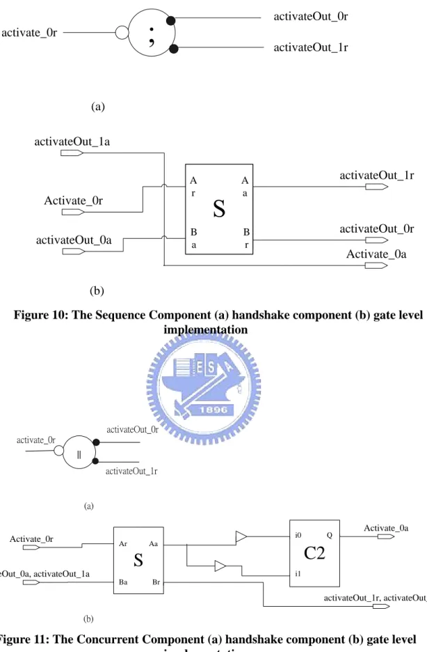
Figure 10: The Sequence Component (a) handshake component (b) gate level implementation ... 12
Figure 11: The Concurrent Component (a) handshake component (b) gate level implementation ... 12
Figure 12: The Variable Component (a) handshake component (b) gate level implementation ... 13
Figure 13. Pipelined 8051 Top Level ... 15
Figure 14. The IF stage... 16
Figure 15. The ID stage ... 17
Figure 16. The OF stage ... 18
Figure 17. The EXE stage... 20
Figure 18. The WB stage ... 23
Figure 19. The Memory interface... 24
Figure 20. The hazard situation... 26
Figure 21. The FPGA design flow of balsa ... 32
Figure 22. The VLSI design flow of balsa ... 33
Figure 23: SA8051 behavior simulation environment ... 35
List of Tables
Table 1. The advantage and Disadvantage of Asynchronous Design... 2
Table 2: Instruction execution scheme... 7
Table 3. The Read Control Signal ... 19
Table 4. The Opcode control signal... 21
Table 5. The Write Back control signal ... 22
Table 6. The instruction Execution Stage ... 25
Table 7. The performance of executing GCD program... 37
Table 8. The Cost of Every Part of 8051 ... 38
Chapter 1. Introduction
The objective of this thesis is to design and implement a pipelined asynchronous 8051 microprocessor. 8051 is a CISC ISA, thus the instruction set is complicated. To design a pipelined 8051, we analyzed the instruction sets, found its regulation, and proposed a new architecture for 8051 microprocessor. The remainder of this chapter is briefly introducing the asynchronous design, and the Balsa tool.
1.1 Motivations
A digital system is designed as a collection of subsystems, and each it performs a different computation and communication with its peers to exchange information. When communication transactions take place, the whole systems need to be synchronized in order to guarantee the validity of data exchanged.
The dominant synchronization technique is global clock. The clock period defined the time when communication transition can take place; therefore the clock period must longer then the execution time of every systems, and the clock distribution is becoming an increasingly cost issue.
Thus, a different type of design- asynchronous circuit design is attracted more and more research interest. Furthermore, several asynchronous circuits design methodologies have been proposed[13]. A number of asynchronous processors have been developed including Asynchronous ARM RISC processor (AMULET1, AMULET2e, AMULET3)[8][11][12] in University of Manchester and Lutonium processor in CalTech [9].
It is widely known that the 8051 is the most popular microprocessor. Therefore, we implemented it with the pipeline method and asynchronous design to increase its performance.
1.2 Asynchronous Design
Synchronous circuit design is the major method in circuit design because it is widely used and full of design experiences. However, asynchronous circuit has some advantages over synchronous circuit. First, asynchronous circuit is average case performance, because it does not the clock to trigger the action and every component can work at its speed. Second, asynchronous circuit has no clock signal, therefore no power consumption needed for the clock. It can also almost attain zero power consumption in its idle state because almost all
components are idle. Third, asynchronous circuit is easy to modular design. Every component can be connected by the same communication protocol. Fourth, asynchronous circuit can avoid the clock skew problem. Fifth, without the clock distribution, asynchronous design is low EMI (Electromagnetic Influence) problem.
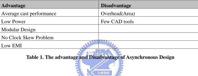
But, asynchronous circuit still has some problems over synchronous circuit. First, without the clock control, asynchronous circuit needs more control signals, resulting in increasing in area. Second, there are few CAD tools to support asynchronous design and test, and this make it harder and longer to design the asynchronous circuit. That is a big challenge. The advantage and disadvantage of asynchronous design is shown in Table 1.
Advantage Disadvantage
Average cast performance Overhead(Area)
Low Power Few CAD tools
Modular Design
No Clock Skew Problem Low EMI
Table 1. The advantage and Disadvantage of Asynchronous Design
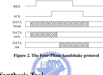
The majority of modern asynchronous circuit design techniques are based on the use of handshaking to communicate between units. Handshaking means the communication protocol between two connected components. There are two types of handshake protocol, two-phase and four-phase. The two-phase handshake protocol is shown in Figure 1. The falling and rising edge of request and acknowledge are active signals. The periods between a request and its acknowledgement forming the handshake itself, and the period between an acknowledgement and the next request, forming the idle phase. The data transition must obey the setup time and hold time constraint.
Another type of handshake is four-phase. In this protocol, only the rising edge is the valid active transition. Four-phase handshake is easier in CMOS design because only the rising edge of signal can be the handshake phase, and the falling edge to reset the handshake signal. There are three type of four-phase handshake protocols distinguished by the data transition period, ie, broad, early, and late as shown in Figure 2.
Figure 1. The Two-phase handshake protocol
Figure 2. The Four-Phase handshake protocol
1.3 Balsa Synthesis Tool
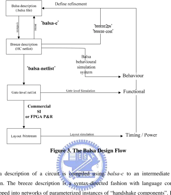
Balsa is an asynchronous hardware description language developed by the Manchester University. It can be directly compiled into several Handshake Components. We can use the Balsa HDL to describe the behavior model of our circuit, and then compiled it into the most popular hardware description language such as Verilog or VHDL. The overview of balsa design flow is shown in Figure 3.
Figure 3. The Balsa Design Flow
Balsa description of a circuit is compiled using balsa-c to an intermediate breeze description. The breeze description is a syntax-directed fashion with language constructs being mapped into networks of parameterized instances of “handshake components”. Each of “handshake components” has a concrete gate level implementation
A number of tools are available to process the breeze handshake files. The balsa-netlist automatically generates CAD native netlist files, which can be fed into the commercial CAD tools that further synthesize the netlist to the fabricable layout. Balsa support three commercial CAD systems: Compass Design Automation tools from Avant, Xilinx FPGA
design tools and Cadence Design Framework II.
Balsa supports three back-end protocols for use with each technology: bundle-data scheme using a four-phase-broad/reduced-broad signaling protocol, a delay-insensitive dual-rail encoding and a delay-insensitive one-of-four encoding. The bundled-data back-end should be faster and smaller, but needs more careful post-layout timing validation. The two delay-insensitive schemes are larger and slower but should be more robust to layout variations.
1-4 Organization of this thesis
In this thesis, we will illustrate the related work in chapter 2 including the overview of the synchronous 8051, and the basic cells in Balsa synthesis system. In chapter 3 we will illustrate the design of PA8051 modeled by Balsa. In chapter 4 we will illustrate the implementation and verification of PA8051. In chapter 5 we will illustrate the results of simulation. Finally, a brief conclusion and future work are discussed in chapter 6.
Chapter 2. Related Work
2.1 Overview of 8051
The architecture of the original synchronous 8051 has three buses: IB, PB, PARB bus. IB-bus acts as the communication channel between any two registers. PB-bus acts the communication channel among PAR (Program Address Register), Buffer, PC Incrementer, PC and DPTR. PAR sent out program address on PAR-bus. The width of the IB bus is 1 byte while the PARB and PB are 2 bytes. The internal memory consists of on-chip ROM and on-chip data RAM. The on-chip RAM contains a rich arrangement of general-purpose storage, bit-addressable storage, register banks, and special function registers (SFR). The registers and input/output ports are memory mapped and accessible like any other memory location and the stack resides within the internal RAM rather than in external RAM. SFRs take care of the communication between CPU and peripherals. There are four bidirectional ports (P0 – P3) for communication to and from the outside world. The architecture of synchronous 8051 is shown in Figure 4.
The 8051 also includes bit operations, which only affect single bit in a given registers. Only some locations of the internal RAM are bit-accessible including address from 20H to 2FH and some SFRs. Internally, the bit operations are performed by reading the whole byte from internal memory, modifying the single bit, and then writing the value back in the same operation cycle.
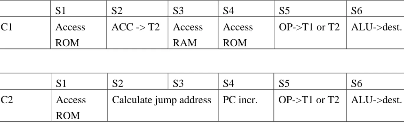
Table 2 is the instruction scheme of the synchronous 8051. Each instruction is executed in one, two or four machine cycles. A machine cycle consists of a sequence of 6 states, numbered S1 through S6. Each state time lasts for two oscillator periods. A machine cycle is totally 12 oscillator periods. Therefore, with an internal clock frequency of 12 MHz the performance will be below 1 MIPS. In each state of the execution scheme a specific action takes place. The one-cycle instructions execute the first machine cycle C1, while the two-cycle instructions execute C1 and C2 consecutively. The scheme results in many redundant cycles during execution because not all actions are required in one machine cycle. For example, two program fetches are generated during each machine cycle, even if the instruction being executed does not require it.
S1 S2 S3 S4 S5 S6 C1 Access ROM ACC -> T2 Access RAM Access ROM OP->T1 or T2 ALU->dest. S1 S2 S3 S4 S5 S6 C2 Access ROM
Calculate jump address PC incr. OP->T1 or T2 ALU->dest.
Table 2: Instruction execution scheme
2.2 Overview of Pipeline Architecture
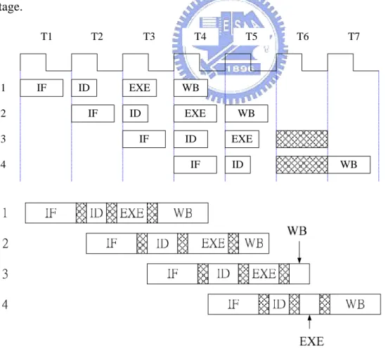
The pipeline architecture is a most commonly used method in microprocessor designs. It can increase the throughput due to the parallel processing of instructions. In asynchronous circuit design, the utility of pipeline can further be increased because of every stage of the pipeline can proceed in its own speed, not the synchronous pipeline worst case performance.
In Figure 5, the two graphs express the difference between synchronous and asynchronous pipeline. We may assume that the pipelined system is divided into four stage; they are IF, ID, EXE, and WB. In synchronous pipeline, every stage must be controlled by the global clock which is set to the slowest pipelined stage. However, in asynchronous circuit, every stage can be proceeded with its own speed. Some instruction may not need all five stages to complete, such as instruction 3 and 4 in Figure 5. The instruction 3 does not need WB stage and the instruction 4 doesn’t need EXE stage. In synchronous pipeline, even the instruction needn’t execution in one stage, but it still need to wait a complete cycle to the next stage. But in the asynchronous pipeline, the instruction can be proceeded quickly to next stage. IF ID EXE WB IF ID EXE WB IF ID 3 2 1 T1 T2 T3 T4 T5 T6 4 T7 EXE IF ID WB
2.3 Balsa back-End
The Balsa back-end generates gate level netlist to import into target CAD systems in order to produce circuit implementations. In this section we will describe some basic cells for Xilinx technology generated by Balsa such as Muller C element and S element. We also describe some handshake components in Balsa synthesis system.
2-3-1 Basic Elements
The gate level netlist generated by Balsa for Xilinx technology only uses some basic cells including AND, OR, NOR, XOR, NADN, BUF, XNOR, INV, FD (D-type flip-flop), FDC(D-type flip-flop with asynchronous clear) and FDCE(D Flip-Flop with Clock Enable and Asynchronous Clear). Every bigger component is composed with these basic cells.
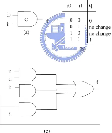
Figure 6: The Muller C-element, (a) symbol (b) true table (c) gate-level implementation
Figure 6 shows the Muller C-element. It is the most common used element in asynchronous circuit. It is a state-holding element like an asynchronous set-reset latch. When both inputs are 0, the output is set to 0. When both inputs are 1 the output is set to 1. For other input combinations the output does not change. A Muller C-element is a fundamental
component that is extensively used in asynchronous circuits. NC2P i0 i1 q i0 i0 i1 q i0 i1 1 0 no change q 0 X 1 1 1 0 (a) (b) (c)
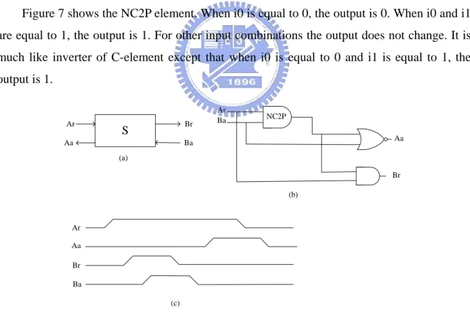
Figure 7: The NC2P-element (a) symbol (b) true table (c) gate-level implementation
Figure 7 shows the NC2P element. When i0 is equal to 0, the output is 0. When i0 and i1 are equal to 1, the output is 1. For other input combinations the output does not change. It is much like inverter of C-element except that when i0 is equal to 0 and i1 is equal to 1, the output is 1. Ar Ba Aa Br S Ar Aa Br Ba Ar Aa Br Ba (a) (b) (c) NC2P
Figure 8: The S-element (a) symbol (b) gate-level implementation (c) handshaking protocol
request/acknowledge handshake pairs – ‘Ar’/’Aa’ and ‘Br’/’Ba’. In Balsa system it replaces the “inverter of C-element” with “nc2p”. Hence, it can reduce the number of gates because “inverter of C-element” uses 3 AND gates, 1 OR gate and 1 Inverter but “nc2p” uses 2 AND gates, 1 NOR gate and 1 Inverter.
2-3-2 Handshake Components
Balsa has about 40 components that use handshake signaling for communication. Each of “handshake components” has a concrete gate level implementation. In the following section we illustrate some handshake components [2] .
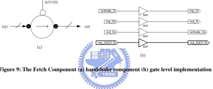
Figure 9: The Fetch Component (a) handshake component (b) gate level implementation
Figure 9 is the Fetch component. This component is the most common way of controlling a datapath from a control tree. Transferrers are used to implement assignment, input and output channel operations in Balsa by transferring a data value from a pull datapath and pushing it towards a push datapath [2].
Figure 10 and 11 are sequence and concurrent component respectively. They form a large part of handshake circuit control trees [2]. They are used to activate a number of commands under the control of activate handshake.
activate_0r activateOut_0r activateOut_1r (a) (b) activateOut_1a activateOut_0r Activate_0r activateOut_1r Activate_0a A r A a B r B a activateOut_0a
Figure 10: The Sequence Component (a) handshake component (b) gate level implementation (a) (b) activateOut_1r, activateOut_0r Activate_0r Activate_0a
S
Ar Aa Br Ba activateOut_0a, activateOut_1aC2
i1 Q i0 activate_0r || activateOut_0r activateOut_1rFigure 11: The Concurrent Component (a) handshake component (b) gate level implementation
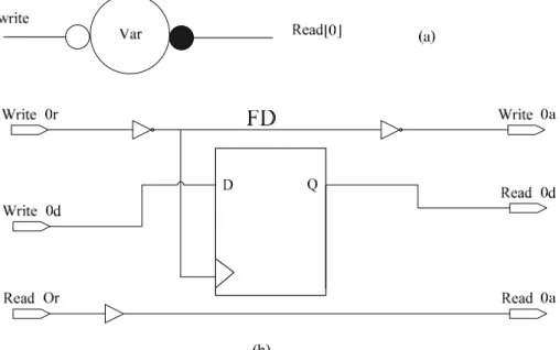
Figure 12: The Variable Component (a) handshake component (b) gate level implementation
Figure 12 is the variable component. It uses D-type flip-flop to store data. The source of clock is the signal write_0r. When a piece of data is needed to be stored, the signal write_0r is set and then the signal is reset. When a piece of data is needed to be read, the signal read_0r or read_1r is set. It is natural to achieve the effect of gating clock.
2-4 Concluding Remarks
In this chapter we introduce the synchronous 8051 architecture. 8051 is a complex instruction set computer. It has variable-length instructions from one to three bytes. Each state of a machine cycle uses the bus. We then introduce the concepts of asynchronous pipeline. Finally we illustrate the Balsa back-end. Balsa synthesis system is composed of about 40 components. Each can be translated into gate level netlist. They use handshaking protocol for communication.
Chapter 3. Design of PA8051
This chapter describes the design of PA8051. This PA8051 consists of six main part, ie, IF, ID, OF, EXE, WB, and MEM, this six parts work parallel with the communication channel connected between them. But MEM is not part of the pipeline, it is a shared component in the architecture. This chapter introduces the top view of PA8051 in the first, and then describes the six main components of the processor.
3.1 The architecture of PA8051
The architecture view of PA8051 is described in figure 13. All of the operations can be completed in the five execution stage and memory unit. The IF(instruction fetch) stage is the fetch unit to get instruction from the program ROM. The ID(instruction decode) stage is the decode stage, responsible for decoding instructions to several control signals. The OF(operand fetch) stage is the fetch unit to get data from data memory and register, and providing the data for the next execution stage. The EXE(execution) stage is the main stage of execution, containing one Multiplier, one Divider, and one general ALU. The WB(write back) stage collects the result from EXE stage, and writes back to destination memory address and register. The MEM(memory) unit contains three part. RAM_READ_ARBITOR arbitrates the two read port from ID and OF. MEM_INTERFACE is responsible for the communication with memory data. MEM is the memory data, which contains a 128-byte memory and special function register (SFR).
Figure 13. Pipelined 8051 Top Level
Following code is the top level process of PA8051. Every component is connected between internal channels.
procedure SA8051_IFIDOF(
output p0,p1,p2,p3 : byte ) is
channel IF_2_ID_data : byte channel IF_2_mem_addr : Address channel ID_2_IF_addr : Address …….
BalsaMemory_interface(IF_2_mem_addr,read,…)|| IF(mem_2_IF_data,ID_2_IF_addr,…) ||
ID_top(IF_2_ID_data,jmp,ID_data,…)|| SA8051_OF(ReadS, WriteSin, MEM_OF,…)|| RAM(maddr,wr,mem_in,mem_out,p0,p1,p2,p3)||
MEM_INTERFACE(MemIn,….)|| SA8051_EXE(src1, src2, src3,…)|| SA8051_WB(EXE_WB, …)|| Ram_Read_Arbitor(MEM_data,valid_face_2_arbitor, …)|| end end
3.2 The IF stage
IF stage contains the one ROM interface, two buffers, and one fetch controller. The ROM interface is the interface between program ROM and the processor. It sends the program counter to ROM and fetches the instruction from ROM. These two buffers have 32 bytes storage space performing as a instruction cache to the program memory. When one buffer have been read the at least byte, the fetch control will read the next instruction from another buffer. If both buffers miss, these two buffers will fetch 64 bytes data from the current PC. PC
ID
Instruction ROM INTERFACE buffer1 buffer2 Fetcher ctrl data Address data Address data Address data Address data Address RnW RnWFigure 14. The IF stage
3.3 The ID stage
Opcode:The control signal, used in EXE stage, controls the type of computation.
Read:The control signal, used in OF stage, controls the read signal to SFR, memory and
register.
Write:The control signal, used in WB stage, controls the write back signal to SFR,
memory and register.
The first part of ID stage is ID1, it decides the instruction type of every instruction. If the instruction length is longer than one byte, the data in second or third byte are memory address or immediate data. Therefore we can collect it from ID1 without any operation in the ID2 stage. The jmp signal comes from WB stage, and it is the branch taken signal. If jmp is 1, it means a jump occur. If jmp is 0, it means no jump occur.
Figure 15. The ID stage
3.4 The OF stage
The OF stage is the stage providing the source data to EXE stage. There are five main sources, ACC, register, register indirect, memory, and immediate data. Many instructions require the data from two of these five types of sources. Some instructions may need to calculate the write back address in this stage, such as some register address and register indirect address. Therefore there are many different operations in this stage controlled by the ReadIn signal.
Figure 16. The OF stage
ReadIn is the data and ctrl bundle used in OF stage, including control, register address, memory address and immediate data. The following OF_Read type is the data type of ReadIn signal. And table 3 is the ReadCtrl signal.
type OF_Read is record maddr:byte; raddr:3 bits; immed:byte; ctrl:ReadCtrl end
Type Operation Example
ACC Read ACC SWAP A
REGI Read Register indirect MOV A,@Ri ACC_REG Read ACC and Register ADD A,Rn ACC_REGI Read ACC and Register indirect ADD A,@Ri ACC_MEM Read ACC and Memory data ADD A,dir MEMB Read Memory bit address data JBC bit,rel REG_MEM Read Register and Memory data MOV @Ri,dir SP_SPI Read SP and SP indirect POP dir SP_MEM Read SP and Memory data PUSH dir
XCH_R Read ACC and Register XCH A,Rn
XCH_RI Read ACC and Register indirect XCHD A,@Ri XCH_M Read ACC and Memory data XCH A,dir
DPTR_ACC Read ACC and DPTR MOVX @DPTR, A
ACC_IMM Read ACC and immediate data ADD A,#data
MEM Read Memory data MOV dir,dir
MEM_IMM Read Memory and immediate data ORL dir,#data REG_IMM Read Register and immediate data CJNE Rn, #data ,rel REGI_IMM Read Register indirect and immediate data CJNE @Ri ,#data ,rel
DPTRI Read DPTR indirect MOVX A, @DPTR
ACC_REGB Read ACC and Register address MOV Rn,A FETCH_REG Read Register address MOV Rn,#data IMM_REGB Read Register and immediate data MOV @Ri,#data
REG_WB Read Register data DJNZ Rn,rel
MEM_WB Read Memory data DJNZ dir,rel
IMM Read immediate data MOV dir,#data
DPTR Read DPTR INC DPTR
IMM16 Read immediate 16 bit data MOV DPTR,# data 16
NO CPL C
Table 3. The Read Control Signal
3.5 The EXE stage
The EXE stage processes the data from OF stage. It contains two register PSW and one-bit color bit. Register PSW provides the carry and auxiliary carry data in this stage and color bit is used to manipulate the control hazard.
Figure 17. The EXE stage
The opcode is the control signal used in EXE stage, table 4 shows the opcode number and its example.
OPCODE Example
MUL MUL AB
DIV DIV AB
NOP RET
MOV MOV A,@A+PC
ADD ADD A,#data
ADDC ADDC A,#data
SUB SUBB A,#data
NOT CPL A
AND ANL A,#data
XOR XRL A,#data
OR ORL A,#data
RL RL A
RR RR A
RRC RRC A
SWAP SWAP A
XCH XCH A,Rn
XCHD XCHD A,@Ri
INC INC dir
DEC DEC dir
DA DA A
DJNZ DJNZ Rn,rel
CJNE CJNE A, #data, rel
CMPZ JZ rel CMPNZ JNZ rel INC16 INC DPTR BCMPZ JB bit,rel BCMPNZ JNB bit,rel BCMPNZC JBC bit,rel CLRA CLR A JC JC rel JNC JNC rel CPLB CPL bit CLRB CLR bit
SETB SETB bit
MOVB MOV bit,C
CPLC CPL C
CLRC CLR C
SETC SET C
ORC ORL C,bit
ANLC ANL C,bit
ORLNC ORL C,/bit
ANLNC ANL C,/bit
MOVC MOV C,bit
Table 4. The Opcode control signal
3.6 The WB stage
The control signal WriteCtrl is the control signal used in WB stage. Table 5 shows the signal and its operation. The following MemWrite type is the write back data and control to Memory.
type MemWrite is record
sfr:byte; --data mem: byte; --data maddr:byte; --address ac:bit; cy:bit; ov:bit; ctrl:MemWCtrl --ctrl end
Type Operation Example
ACC Write ACC ADD A,#data
MEM Write Memory INC dir
MEM_WB Write Memory ORL dir,#data
MEMWB Write Memory bit CPL bit
SP_MEM Write Memory and SFR PUSH dir ACC_MEM Write ACC and Memory XCH A,dir
DPTR Write DPTR MOV DPTR,# data 16
NO NOP
JMP Jump JMP @A+DPTR
CJMP Jump CJNE A, #data, rel
JMP_MEM Jump and write memory DJNZ dir,rel JMP_MEMWB Jump and write memory bit JBC bit,rel
CY Write carry CPL C
Figure 18. The WB stage
3.7 The Memory and Register Interface
The Memory and Register Interface is the control unit between ID and OF and Memory. Because both of the two stage ID and OF can read memory data, a RAM_READ_ARBITOR is used to arbitrate the data read from ID or OF stage. The MEM_INTERFACE arbitrate the read or write signal from RAM_READ_ARBITOR and WB, and then fetch data from Memory or write data into memory. Two register ACC and PSW are located in MEM_INTERFACE because these two registers are frequently fetched. In order to reduce the fetch time, they are not in the MEM unit. The lock signal comes from OF stage, and it tells MEM_INTERFACE what the memory address or SFR needs to be locked. This mechanism prevents the data hazard. If the data is locked, then the valid will be 0. When the valid bit is 0, RAM_READ_ARBITOR sends the control signal back to MEM_INTERFACE, until it gets the correct data, that is, valid is 1. The following code segment describes the mechanism in the RAM_READ_ARBITOR unit.
loop
MemRead <- read_ctrl || data -> dataT||lock<-lockT||valid->validT while(validT /=1)
end;
3.8 The instruction execution stage
All the instruction are executed in the order IF, ID, OF, EXE, and WB. However, not all the instructions need to completely use the five execution stages. Table 6 shows the operation stages of all the 256 instructions. Only 21 instructions execute with IF and ID stage, because these instructions are unconditional jump and need no ALU operations. They can be completed in first two stages. Other instructions need all the five stages to complete execution. Although some instructions such as MOV are no operation in EXE stage, we can just connect the OF output to WB stage, we didn’t do so. With this design, the WB stage can receive the data both from OF and EXE. If the OF stage output data is faster then that of EXE stage, there will be an out-of-order completion situation in the design, therefore we need more control to handle the problem.
As a result, we set all the instruction in the execution order of IF-ID-OF-EXE-WB. If one instruction doesn’t need one execution stage, a bypass signal will be sent into next stage. The following code is part of the code in the EXE stage to deal with MOV.
|NOP..MOV then dest1:=src1 || dest2:=src2. dest_1 <- dest1 || dest_2 <- dest2
Execution stage Number of instructions Example
IF-ID 21 NOP, AJMP
IF-ID-OF-EXE-WB 235 CPL bit, ADD, MOV…..
Table 6. The instruction Execution Stage
3.9 The Hazard control and data forwarding
Hazards are serious problems may be happened in pipeline machine; and they need to be avoid or solved. Hazard has two type may be found in PA8051, data hazards and control hazards. Data hazards happened in the data dependency of consecutive instructions. Control hazards may be happened in the branch occurring during pipeline execution. We classified data hazard into three types. The first type data hazard can be solved with forwarding mechanism, but the second and third types of data hazard, only can solve with stall. Data hazards will only happen in two consecutive instructions to access the same memory address, and the hazard may also be resolved by inserting any one non-related instruction between these two instructions.
Figure 20. The hazard situation
Figure 20 shows an example of the data hazard. It shown that the first and second instruction have data dependency on A. When the second instruction is in OF stage, the first instruction is in EXE stage, and thus the second instruction can not correctly fetch the data at this moment. However, the third instruction is no data hazard, because when it is in OF stage, the first instruction is in WB stage, there is no data hazard happened.
Because our design is implemented with asynchronous circuit and not all instructions, may be executed in the sequence like what is shown in Figure 20; and furthermore the execution time of every stage may be different, is there no data hazard between the first instruction and third instruction with different instruction execution sequence? The answer is yes! In our design, when the third instruction enters OF stage, the second instruction must be in EXE stage, and when then the second instruction enters EXE stage, the first instruction must in WB stage. Therefore, when the third instruction enters OF stage, the first instruction must be already in WB stage. As a result, the first instruction must be finishing write back before the third instruction begins to fetch data.
3.9.1 Data Hazard
The only data hazard is read after write. If there are two consecutive instruction, the first instruction writing and second instruction reading the same location, the second instruction will read the old data. There are three types of data RAW hazard:
Type 1:Solved with data forwarding
ADD A, #data ADD A, Rn
the dest1 register in EXE stage and can be simply used as the input of ALU operation for the second instruction. The forward control generated in the MEM_INTERFACE unit. There are five types of forward operations, SRC121, SRC221, SRC122, SRC122, and SRC1_2. SRC121 means previous destination 1 forward to source 1, and SRC 221 means previous destination 2 forward to source 1. The following code segment shows the forward mechanism in EXE stage. case forward of SRC121 then src1:= dest1 |SRC221 then src1:= dest2 |SRC122 then src2:= dest1 |SRC222 then src2:= dest2 |SRC1_2 then src1:=dest1 || src2:=dest2 |NO then continue else continue end;
The forward signal is sent by MEM_INTERFACE unit. In OF stage, the memory address need to be lock are generated and sent to MEM_INTERFACE. The lock signal contains the lock memory address and control. In MEM_INTERFACE, four register used to control the lock and forward mechanism. The register RD11 and RD12 indicates the lock address of current instruction. The register RD21 and RD22 indicates the lock address of previous instruction. Whenever an instruction retrieves the correct data, then it locks the memory. The following is the code fragment of lock memory. The RD11 and RD12 changes to current lock data, and previous lock data move to RD21 and RD22.
shared LOCK_MEM is begin case lockT.ctrl of ACC then RD21:=RD11||RD22:=RD12; RD11:=R_ACC||RD12:=255
|MEM then
RD21:=RD11||RD22:=RD12; RD11:=lockT.addr ||RD12:=255 ……
In our design, only two successive instructions may have data hazard, and therefore we need to check RD11 and RD12. If RD11 is the address we want to fetch, just forward. The following code shows some code segment in MEM_INTERFACE, and three types of operation will occur, forwarding from destination 1 or destination 2, and fetch ACC. Note that lock memory is required after fetch data.
shared RESET_LOCK is begin if(RD21=255) then RD11:=255||RD12:=255 else RD21:=255||RD22:=255 end end case MemRead.ctrl of ACC then if(RD11=R_ACC) then forward<-SRC121||NULL_OUT()||LOCK_MEM() |RD12=R_ACC then forward<-SRC221||NULL_OUT()||LOCK_MEM() else
data<- (#ACC @ #C0_8@ #C0_8 as 24 bits)||valid<-1||LOCK_MEM()||forward<-NO end
……
Type 2:Solved with stall
In this type, the operand needs to be fetched in OF stage, but at the meantime, the previous instruction is in EXE stage and the new operand value is not calculated. Therefore, we need to stall the pipeline in this situation.
INC R1
ADD A,@R1
read the R1 value. So we need to wait for the first instruction to complete and then to execute the second instruction. We solved this problem with the memory lock mechanism in MEM_INTERFACE and RAM_READ_ARBITOR. The following code fragment is the control of read register of indirect data. First we calculate the memory address in Extract_RegR(). If this memory is locked, we send the NOT_VALID() signal to RAM_READ_ARBITOR. RAM_READ_ARBITOR will continuously send signal to MEM_INTERFACE until it gets the correct data. The stall mechanism is easily to achieve.
case MemRead.ctrl of |REGI then
Extract_RegR(); If(error=1) then NOT_VALID()
|(RD11=raddr or RD12=raddr) then NOT_VALID() else wr <-0 || addr<-raddr ||in_data1->tmp0; if(RD11=tmp0) then forward<-SRC121||NULL_OUT()||LOCK_MEM() |RD12=tmp0 then forward<-SRC221||NULL_OUT()||LOCK_MEM() else FETCH_REGI(); TO_OF <- (#tmp1 @ #C0_8@ #tmp0 as 24 bits)||valid<-1|| LOCK_MEM()||forward<-NO end end
Type 3:Solved with stall
In this situation, the first instruction changes the register select bit RS0 or RS1 in PSW, and then the next instruction need to read register. Because the next instruction needs to wait the correct RS0, therefore stall is required in this situation. The situation will happen when the following code execute.
SETB C.RS0 MOV dir, Rn
The following code segment shows the register address generating procedure. If PSW is locked, then error=1, the NOT_VALID data will be sent to register read control.
shared Extract_RegR is begin
if(RD11=R_PSW or RD12=R_PSW) then error:=1
else
raddr := (#OFtoMEM.raddr@ #psw[3..4] @ #C0_3 as byte)||error:=0 end
end
3.9.2 Control Hazard
Control hazard happens when any jump instruction appears in the program. When jump occurs, the coming instructions in the pipeline must be flushed. To solve this problem, we use the color bit method. We add a bit in every instruction named color bit. and a one bit register(color register) stores the current color information in the EXE stage. Every time when jump occurs, the color register complement it. Therefore when the coming instruction executed in the EXE stage, it can check the value of its color bit with color register. If the value is different, a jump is occurred and then this instruction needs to be flushed. The following code shows the operation in EXE stage.
if(color=colorT) then case aluop of MUL … |DIV … else send NOP end
Chapter 4. Implementation and
Verification
This chapter contains two parts. First, we illustrate our design flow for asynchronous implementation on FPGA and VLSI. Second, we illustrate the behavior simulation.
4.1 The VLSI and FPGA design flow of
asynchronous circuit using balsa
The PA8051 core is modeled with Balsa language, and then compiled into a collection of “handshake components” with the balsa-c cmpiler. Each of these components has a concrete gate level implementation; and then use the balsa-netlist tool can automatically generate them into Verilog for Xilinx or other target synthesis tools.
The following steps are the design flow for FPGA. The Verilog netlist generated by balsa-netlist is converted into a netlist of basic gates in the synthesis step of the design flow. The netlist may be optimized using technology-independent logic minimization algorithms. However, we must avoid the logic minimization for hazard free circuits and buffers generated by balsa-netlist. We should add the constraint “keep hierarchy” to avoid the logic minimization. Then the synthesized netlist is mapped to the target device using a technology-mapping algorithm. The placement algorithm maps logic blocks from the netlist to physical locations on an FPGA. On the placement has been done, the routing algorithm determines how to interconnect the logic blocks using the available routing. The final output of the design flow is the FPGA programming file, which is a bit stream determining the state of every programmable element inside an FPGA. The design flow is shown is figure 21.
Balsa description
FPGA Programming
file
Timing Simulation
Balsa-c
Breeze description
Balsa-netlist
Verilog netlist for
Xilinx
Synthesis
MAP
Placement & Routing
Behaviour Simulation
Function Simulation
Figure 21. The FPGA design flow of balsa
The VLSI design flow of balsa has some difference on FPGA design. First, the balsa-netlist do not support the Synopsys technology, we only can use the “ Example”
Synopsys Design Compiler to synthesize the Verilog model. After synthesizing, we do the functional simulation with Modelsim. After functional simulation, we do the place and route with SOC Encounter, and export the layout GDS file.
4.2 Implementation Issues
Compilation from Balsa programs to Xilinx netlist proceeds in two steps. In first step, handshake circuits form the intermediate architectures. An important characteristic about this compilation is that it is transparent, which allows feedback about important performance characteristics such as performance, area, timing and testability to be generated at the handshake circuit level and to be presented to the VLSI programmer at the Balsa level. When the designer is satisfied with the performance of the Balsa program, the corresponding handshake circuit is expanded into a gate-level netlist with target technology. At this level the design can be translated to Verilog HDL and simulated it to obtain more accurate performance figures using commercial EDA tools.
We choose four-phase bundled data protocol to implement the handshake circuit instead of dual-rail encoding in order to reduce the area cost. The Balsa provided some technology for implementations. If we choose Xilinx ISE, the circuits are implemented only using the Xilinx standard cells such as AND, OR, Inverter gate and flip flop. If the target synthesize tools are not supported such as Synopsys Design Compiler, we can use the “Example” technology which translated the circuit to some basic cell, and we need to modified the basic cell with the standard cell in the target synthesize tool.
It should be noticed that the synthesis tool could do logic minimization but it must be avoided. The asynchronous system added some buffer or redundant circuit to ensure hazard-free. They can not be minimized. We can avoid this situation by adding the constraint “keep hierarchy” on the handshake modules.
RAM and ROM are not modeled by Balsa language. We can implement them using the block RAM on FPGA or using the standard RAM in VLSI. Until now all instructions can be executed except MOVX. The peripherals are not considered such as timers and UART.
4.3 Verification
The environment used to do behavior simulation for PA8051 is illustrated in figure 23.
The ROM model is the predefined procedures in Balas as shown in figure 24. We assign the address width and data width to determine their size. The ROM size is 4K bytes. The contents of the ROM are loaded during initialization as 8-bit quantities in the hexadecimal format from a hexadecimal file. A hexadecimal file is translated from a C program by KEIL tool [6].
outputs the instruction code. When the processor wants to write data, it sets the signal rNw and sends out the address and the data.
The 8051 simulator executes the instructions in the hexadecimal file. The execution results are compared with the contents of the RAM. If the results are not equal, we must modify the code of the processor.
SA8051 (Balsa)
ROM Model (Balsa)
8051 HEX file 8051 Object Code Source file (C)
8051 Simulator
Execution Result=
Yes Correct No KEIL-oh51 KEIL-c51 KEIL-a51 KEIL-bl51Chapter 5. Result
5.1 Simulation Result
We have successfully executed some GCD Codes in PA8051 using the verification method in Figure 23. The behavior simulation is passed. But the functional simulation was not yet completed.
The performance comparison between asynchronous 8051[14] and PA8051 was shown in table 7. When the SA8051 and PA8051 executing the same GCD program in balsa development environment, the estimated time can be calculated. The result is that the SA8051 spend 2.74 times over PA8051. Therefore, in behavior simulation, PA8051 have better performance than SA8051, the speedup is about 2.74.
In our design, we divided the processor into five stages, theoretically there will be 5 speedup compared to non-pipelined design. Because the five stages are not balanced, some stages are longer than the other stages. Furthermore, the pipelined architecture increasing the control signals overhead. Thus, PA8051 can’t totally benefit from the pipelined structure, but the 2.7 speedup is greatly better than SA8051.
GCD (estimated time) Speedup
SA8051 76411420 1
PA8051 27851320 2.74
Table 7. The performance of executing GCD program
5.2 Area Cost
PA8051 was synthesized with Xilinx ISE, and the gate and path delay of every part of PA8051 is shown in table 8. The ID stage is the most dominant stage of all part of the design, spend half of the total cost PA8051.
Table 9 is the comparison of synchronous 8051 and asynchronous 8051[14] and PA8051, the asynchronous design is much bigger than the synchronous one. The area overhead mainly comes from the handshake circuit in each handshake component. The hazard free circuit is employed in order to assure the circuit validity. The circuits of the completion detection on
the control path which need large C element also result in the area overhead.
Another reason is due to the CAD tool. There are no commercial CAD tools for the asynchronous circuits. The synchronous CAD tools can do some optimization techniques for the speed and area such as logic minimization and retiming. However, the asynchronous tool Balsa just does transparent compilation and does not do any optimization on the asynchronous circuits.
The other extra area overhead of pipelined asynchronous 8051 comes from several aspects. First, every stage has its own control code for operation, and every stage has a big multiplexer to choose the action. But in non-pipelined version, the following action is determined after instruction decoding. This operation does not need many multiplexers. Second, the control code of every stage is too big. Every stage needs a control code to choose the correct action; however, the bigger control code, the more complicated related control circuit will be. For example, opcode in EXE, there are 44 types, and therefore a 1-of-44 multiplexer must be generated. The cost is very big.
slice gate minimum path delay(ns)
IF 1007 13987 757 ID 5353 61973 721 OF 564 7086 34 EXE 1284 16938 174 MEM_INTERFACE 1098 13217 125 RAM_READ_ARBITOR 57 1051 28 WB 232 2977 40 TOTAL 9595 117229
Table 8. The Cost of Every Part of 8051
Slice Gate
Synchronous 926 16688
Asynchronous (SA8051) 2155 26942 pipelined asynchronous (PA8051) 10226 123510
Chapter 6. Conclusion and future work
We designed and implemented a pipelined asynchronous 8051 microprocessor. In our design, except MOVX, the overall 8051 instructions can be executed correctly, but the IO and interrupt mechanisms were not implemented yet.
Our proposed pipelined 8051 PA8051, compared to SA8051, after executing GCD program, have 2.74 speedup. We have a preliminary result in using pipelined to increase performance. Although we should execute more programs to verify the performance, we almost can confirm that PA8051 have better performance than SA8051 and the speedup is above 2.
The capabilities of FPGAs have increased to the level which makes it is possible to implement a complete computer system on a single FPGA chip. The main component in such a system is a soft-core processor. In addition, the VLSI design with balsa development environment still has some limitations, and the most important of all is that the supported EDA tools that can correctly co-worked with are not sufficient.
The thesis offers the following contributions:
z The architecture of the PA8051 modeled by Balsa is described. Some design issues for Balsa language is also described.
z The new defined architecture for 8051 was developed. Future work for our pipeline asynchronous 8051: z Performance evaluation on FPGA or VLSI design z Adding additional IO and peripherals
References
[1] A. Bardsley, D. A. Edwards, “The Balsa Asynchronous Circuit Synthesis System” 2000. University of Manchester
[2]A. Bardsley, "Implementing Balsa Handshake Circuits," 2000. University of Manchester [3] Doug Edwards, Andrew Bardsley, Lilian Janin & Will Toms“Balsa : A Tutorial
Guide”, 2004.
[4] Hans van Gageldonk, Kees van Berkel_, Ad Peeters “An Asynchronous Low-Power
80C51 Microcontroller”, Philips Semiconductors, 2001.
[5] I.E. Sutherland, “Micropipelines”, Communications of the ACM, Vol.32, Number 6, June 1989, pp 720-738.
[6]I. KEIL Software, "8051 Development Tools," 2005.
[7] Je-Hoon Lee, et.al “A novel asynchronous pipeline architecture for CISC type embedded
controller, A8051”, The 2002 45th Midwest Symposium on Circuits and Systems
[8] J.V.Wood et.al “AMULET1:An Asynchronous ARM Microprocessor”, IEEE Transactions on Computers, Volume 46, Issue 4, April 1997 Page(s):385 – 398
[9] Martin, A.J.,et.al”The Lutonium: a sub-nanojoule asynchronous 8051 microcontroller”, Asynchronous Circuits and Systems, 2003. Proceedings. Ninth International Symposium Page(s):14 – 23
[10]Q.Zhang & G.Theodoropoulos, “Modelling SAMIPS: A Synthesizable Asynchronous
MIPS Processor”, Proceeding of the 37th Annul Simulation Symposium.
[11] S.B.Furber et.al“AMULET2e:An Asynchronous Embedded Controller”,Proceedings of the IEEE Volume 87, Issue 2, Feb. 1999 Page(s):243 - 256
[12] S.B.Furber et.al “AMULET3:A High-Performance Self-Timed ARM Microprocessor”, ICCD '98. Proceedings., Page(s):247 – 252
[13] Spars, J. Furber, S. “Principle of Asynchronous Circuit Design”, 2001. Kluwer Academic Publishers.
[14] Y.T.Chang, “SA8051:An asynchronous soft-core Processor for Low-Power