國立交通大學
光電工程學系 光電工程研究所
碩士論文
偏壓對有機薄膜電晶體氣體感測器之
影響以及相關機制
Influence of bias on OTFT gas sensor
and its sensing mechanism
研究生: 梁芸嘉
指導教授: 冉曉雯 博士
偏壓對有機薄膜電晶體氣體感測器之影響以及相關機制
Influence of bias on OTFT gas sensor and its sensing
mechanism
研 究 生:梁芸嘉 Student:Yun-Chia Liang
指導教授:冉曉雯 博士 Advisor:Dr. Hsiao-Wen Zan
國 立 交 通 大 學
光電工程學系 光電工程研究所
碩 士 論 文
A Thesis
Submitted to Department of Photonics & Institute of Electro-Optical Engineering College of Electrical Engineering and Computer Science
National Chiao Tung University in partial Fulfillment of the Requirements
for the Degree of Master
in
Electro-Optical Engineering June 2007
偏壓對有機薄膜電晶體氣體感測器之影響以及相關機制
研究生:梁芸嘉 指導教授:冉曉雯 博士
國立交通大學
光電工程研究所碩士班
摘要
近年來有機薄膜電晶體氣體感應器已經引起大量的研究,此成果之應用範圍 包含食物品質檢測以及醫療用自我檢測儀器。為了達成能商業量產的價值,我們 需要製造出成本低廉且高度靈敏的感測元件,為了達成這個目的,我們選用有機 電子材料來製造氣體感測器。 現有的相關研究多著重在氣體感測器電流值的變化,對於其他參數如臨界 電壓以及載子移動率卻缺乏討論。我們希望站在元件物理的基礎上更深入的探討 氣體反應的相關機制。 在氣體感應的量測中我們觀察到造成電流值變化的主因是因為臨界電壓的 漂移。隨著氨濃度的增加,臨界電壓值的移動也會更劇烈,但當氨氣移除之後臨 界電壓有恢復到初始狀態的趨勢。故我們認為氨氣與五苯環分子的作用為一種吸 附現象。在這實驗中我們發現一個很有趣的現象:當三顆特性相同的有機元件放在同一個有氨的環境中,不論放置在這環境中多長時間所量測到的初始臨界電壓 都相近,這結果暗示我們氣體感測的行為與閘極偏壓有關。 在長時施加閘極偏壓的氣體感測中,固定施加的偏壓改變氣體濃度,當氨 氣濃度越高臨界電壓變動也增加。若固定氣體濃度施加更高偏壓也會看到相同的 情形。不論是在有無偏壓實驗條件下,氣體擴散模型可以成功解釋氨在五苯環薄 膜中的擴散行為。
Influence of bias on OTFT gas sensor and its sensing
mechanism
Student: Yun-Chia Liang Advisor: Dr. Hsiao-Wen Zan
Institute of Electro-Optical Engineering
National Chiao Tung University
Abstract
Electronic noses have attracted lots of interests in the recent years. It can be
used from food-quality monitoring to medical self-diagnosis kits. For commercial
purpose, we need to produce low-cost and high sensitivity electronic noses. To reach
these targets, we used organic material to fabricate electronic nose.
Most of the previous works focused on the electric current effect alone. In this
work we also studied the effect on threshold voltage 、 mobility, from which we
investigated the mechanism for gas sensing.
In this experiment, we observed that the electric current variation was strongly
influenced by the threshold voltage. When the ammonia concentration was increased,
the threshold voltage became larger. But we noted that the threshold voltage tend to
reaction between ammonia and pentacene is basically an absorption reaction. At the
same time, we observed an interesting phenomenon: we measured three identical
devices that were placed at the same distance from the gas source. When the
measurement was applied on the three devices one after another along with the NH3
sensing time, we observed an interesting event- these three devices had similar initial
threshold voltages no matter how long these devices had been exposed to the NH3 gas.
This result implied that the sensing behavior may have a strong correlation with the
gate bias.
In the experiment of bias stress gas sensing, we applied a fixed gate bias and
varied the ammonia concentration. The threshold voltage became larger with the
ammonia concentration was increased. We observed the same result when we applied
higher gate bias and added a fixed amount of ammonia. Our results showed that
Acknowledgment
首先誠摯的感謝指導教授冉曉雯博士,老師不論在實驗上或者生活上 都給予我很好的建議以及鼓勵,這兩年在老師身上學到很多使我個人也成 長不少,在此獻上最誠摯的謝意。 本論文的完成亦得感謝博士班學長國錫、士欽以及政偉,在實驗上給 予很多的指導以及照顧。尤其士欽學長在我實驗量測上給予相當多的幫 助,讓我得以順利完成實驗。也很高興能與文馨、而康、光明、德倫、廷 遠、皇維、睿志一起度過這難忘的兩年,感謝你們在實驗上以及各方面的 協助。 兩年的生活有苦有樂,謝謝多媒體工程所的詠恬、網路工程所的雅琳、 以及資工所的慧伶陪我一起度過。謝謝你們這一路的關懷以及陪伴,幫助 我度過許多艱辛的時刻。希望不論是出國還是留在國內念博士的你們都會 相當順利。 最後,感謝父母給我最大的空間讓我做自己想做的事。無悔的栽培讓我 順利完成碩士學位。謝謝你們這 24 年來的照顧,謝謝。Contents
Chinese Abstract
Ⅰ
English Abstract
Ⅲ
Acknowledgment
Ⅴ
Contents
Ⅵ
Figure Captions
Ⅷ
Chapter 1. Introduction
1-1 Introduction of Organic Thin Film Transistors (OTFTs) 1 1-1.1 Organic materials 2 1-1.2 OTFT device structure 3 1-1.3 Operating mechanisms of organic thin film transistor 4 1-2 Ammonia sensor and their applications 5 1-2.1 Application areas of ammonia sensors 5 1-2.2 Different types of ammonia sensor 7 1-3 OTFT gas (ammonia) sensor 9 1-4 Motivation 1 0 1-5 Thesis Organization 1 1
Chapter 2. Experimental
2-1 The Fabrication for OTFTs 12
2-4.1. Mobility 15
2-4.2. Threshold voltage 15
2-4.3. Subthreshod swing 16
Chapter 3. Results and Discussion
3-1 The sensing phenomenon under no bias stress 173-1.1 The electrical properties of OTFT gas sensor 17
3-1.2 The recovery phenomenon 18
3-1.3 Gas diffusion model 18
3-1.4 Gas concentration effect 20
3-1.5 The phenomenon of different NH3 exposed time 21
3-2 The phenomenon of bias stress gas sensing 22
3-2.1 The theory of bias stress effect 22
3-2.2 The phenomenon of bias stress gas sensing 24
3-2.3 The gas sensing mechanism under bias stress 26
3-2.3.1 Charge- trapped states 26
3-2.3.2 Dipole molecules 26
Chapter 4. Conclusion
28References
30Figure Captions
Chapter 1
Fig. 1-1 Molecular structure of pentacene.
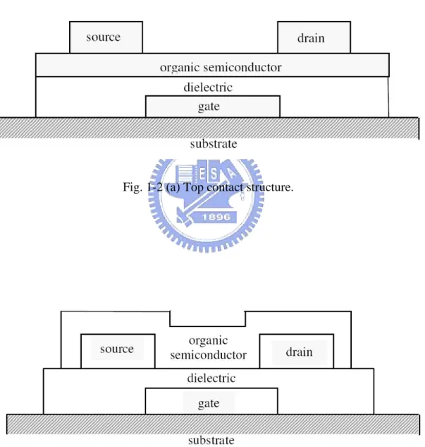
Fig. 1-2 (a) Top contact structure (b) Bottom contact structure.
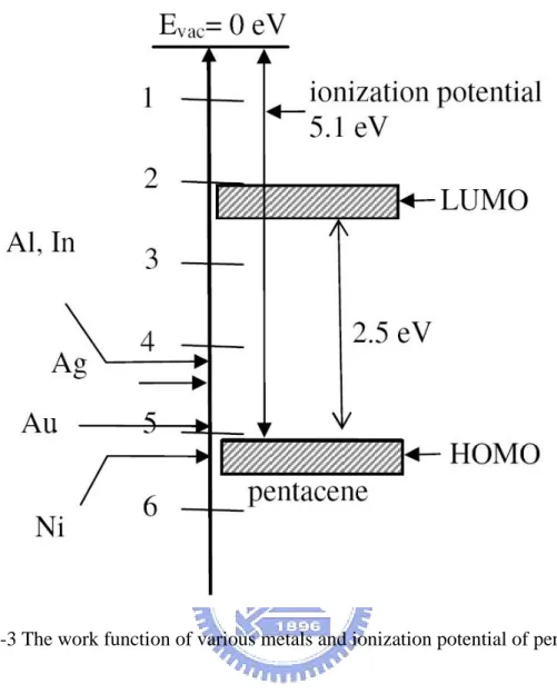
Fig. 1-3 The work function of various metals and ionization potential of pentacene.
Chapter 2
Fig. 2-1 Conventional bottom-gate top-contact OTFTs were used in this experiment.
Chapter 3
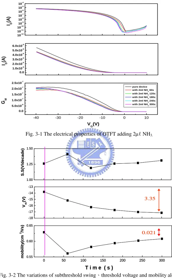
Fig. 3-1 The electrical properties of OTFT adding 2ℓ NH3.
Fig. 3-2 The variations of subthreshold swing、threshold voltage and mobility along
with time in environment of 2ℓ NH3.
Fig. 3-3 The variations of threshold voltage along with time in environment of 2ℓ Fig. 3-4 When NH3 was removed, the threshold voltage tended to recover.
Fig. 3-5 The fitting curve of Fick‘s second law are in the condition of d=10-5 cm and
D=10-12 cm2/s、2*10-12 cm2/s、4*10-12 cm2/s、8*10-12 cm2/s
Fig. 3-6 The fitting curve of Fick‘s second law are in the condition of D=10-12 cm2/s
Fig. 3-8 The dependence of threshold voltage shift on sensing time in the
environments with different NH3 concentrations. The circles are experiment
data. The curves are the fitting result from Fick‘s second law.
Fig. 3-9 The threshold voltage variation of three identical devices measured one after
another in the environment with NH3 gas. The NH3amount injected into the
cotton mass was 2ℓ.
Fig. 3-10 The threshold voltage shift in different bias stress conditions
Fig. 3-11 The threshold voltage shift in different bias stress conditions
Fig. 3-12 The threshold voltage shift in different amount of concentrations with
Vg-Vthini= -7V bias stress.
Fig. 3-13 The threshold voltage shift in the environment of 2ℓ ammonia with different amount of bias stress.
Fig. 3-14 The threshold voltage shift in the environment of 10ℓ ammonia with different amount of bias stress.
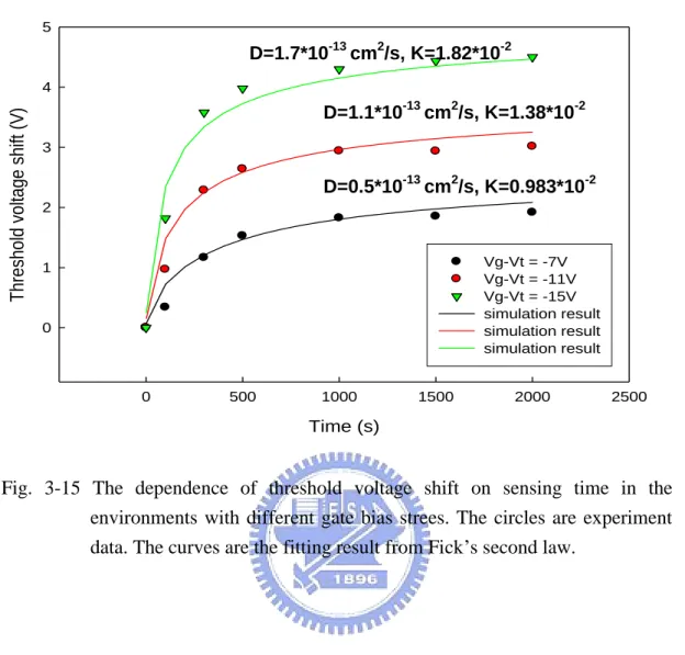
Fig. 3-15 The dependence of threshold voltage shift on sensing time in the
environments with different gate bias strees. The circles are experiment data.
Chapter 1
Introduction
1-1. Introduction of organic thin film transistor (OTFT)
The conductance of organic molecules was discovered in 1940s [1]. It began
from a very small number of preliminary works on conjugated small molecules [2,3]
and polymers[4]. The first transistor based on an organic semiconductor was only
reported in 1986 with a device made on an electrochemically grown polythiophene
film [5]. Polythiophene belongs to the family of the conducting polymers that were
discovered in the late 1970s [6]. The inventors of polyacetylene were awarded the
Nobel Prize in chemistry in 2000. The possibility of fabricating organic thin-film
transistors (OTFTs) with small conjugated molecules was demonstrated in 1989 with
sexithiophene, an oligomer of polythiophene made of sixthiophene rings linked at
alpha position [7]. For a decade, there have been a lot of researches about
better-performing organic thin-film transistors (OTFTs). Now the performances of
OTFTs are comparable to the hydrogenated amorphous silicon TFTs (a-Si:H TFT) [8].
OTFTs have many advantages compared to other electronic devices. The low
frequency identification cards (RFIDs), sensors and electronic paper. For these
reasons, more and more industrial groups have recently initiated research programs in
the field of organic transistors. Until recently, much of the research effort has been
directed at improving the charge-carrier mobility. Several papers have reviewed this
search for better materials and device architecture [9-13].
1-1.1 Organic materials
A number of organic materials such as polythiophene, α- sexithiophene (α-6T)
have been investigated for use in field effect transistors (FETs) [14]. Polycrystalline
molecular solids such as α-sexithiophene (α-6T) or amorphous/semi-crystalline
polymers such as polythiophene or acenes such as pentacene, teracene show the
highest mobilities [15]. Dimitrakopoulos et al [16] shows the evolution of organic
materials and the improvement in their mobilities over the years. Pentacene based
FETs exhibit high mobilities and have been extensively studied. Pentacene is made up
of five benzene rings as shown in Fig. 1-1. It has a sublimation temperature of 300℃.
Well ordered pentacene films can be deposited at low temperatures, this makes it
1-1.2 OTFT device structure
In organic thin film transistor, the organic film can be deposited by evaporation,
spin-on or ink-jet printing. And the devices can be fabricated on a number of
substrateslike silicon, glass and plastic.Figure 1-2(a) and (b)illustrate a widely used
structure of OTFTs: top-contact structure (Fig.1-2(a)) and bottom-contact structure
(Fig.1-2(b)).
In top-contact structure, a heavily doped silicon substrate acts as a gate electrode
for the device. Thermally grown silicon dioxide is deposited on the substrate as gate
insulator. Next, the organic material is deposited on the insulator and the metal is
deposited on the top of the organic semiconductor as the source and the drain
electrodes. Because the organic layer is sensitive to the photolithographic patterning
and chemical etching. The source and drain electrodes are defined through the shadow
mask.
The other popular structure is the bottom-contact structure, in which the organic
layer is deposited directly on the top of the structure. The structure is commonly used
in the field of organic electronics due to the easy fabrication. The entire structure
except for the organic layer can be patterned using photolithography technology.
top-contact structure. The difficulty to obtain well-ordered organic film on metal
electrodes may be the primary reason.
1-1.3 Operating mechanisms of organic thin film transistor
The gate structure of thin-film transistors operates like a capacitor. When a
voltage is applied between source and gate, a charge is induced at the
insulator-semiconductor interface. This charge forms a conducting channel, the
conductance of which is proportional to the gate voltage. At low drain voltages, the
current increases linearly with drain voltage, following the Ohm‘s law. When the
drain voltage is compared to gate voltage, the voltage drop at drain contact falls to
zero and the conducting channel is pinched off. This corresponds to the so-called
saturation regime where the current becomes independent of the drain voltage. In the
transfer characteristic, the current is plotted as a function of the gate voltage at a
constant drain bias. Below a given threshold, the current increases exponentially. This
corresponds to the below-threshold regime. In the above threshold regime, the current
becomes proportional to the gate bias, as expected from the above description of the
operating mode of the transistor.
The Fermi level of gold and the band diagram of pentacene are shown in Fig. 1-3.
source electrode. As can be seen in Fig. 1-3, the Fermi level of gold is far away from
the LUMO level, so that electron injection is very unlikely. Accordingly, no current
passes through the pentacene layer, and the small measured current essentially comes
from leaks through the insulating layer. When the gate voltage is reversed, holes can
be injected from the source to the semiconductor, because the Fermi level of gold is
close to the HOMO level of pentacene. Accordingly, a conducting channel forms at
the insulator-semiconductor interface. The charges can be driven from the source to
the drain by applying a drain bias. For this reason, pentacene is said to be a p-type
semiconductor. However, it should be pointed out that this concept differs from that
of doping in conventional semiconductors, which can be made either n-type or p-type
by introducing a large amount of an electron donating or electron withdrawing
element. Symmetrically, an organic semiconductor will be said n-type when the
source and drain electrodes can inject electrons in its LUMO level, provided electron
transport does occur, i.e., electron mobility is not too low.
1-2. Ammonia sensors and their applications [7]
1-2.1 Application areas of ammonia sensors
Ammonia is an obvious gas in the world. Apart from its natural origin, there are
many sources of ammonia, such as the chemical industry or intensive life-stock.
Subsequently, different application areas for gaseous ammonia sensors are
investigated, such as:
(1) Automotive industry
The application for ammonia sensors in the automotive area is NOx reduction in
diesel engines. Because modern diesel engines cause large concentrations of NO or
NO2 [8.9], people use selective catalytic reduction (SCR) of NOx with NH3 to reduce
the toxic NOx concentrations. The formula is shown in equation (1-1) [10].
4NO + 4NH3 + O2 -> 4N2 + 6H2O (1-1)
But adding too much ammonia causes the other pollution, known as ammonia-slip.
Therefore, measuring the excess ammonia concentration in the exhaust system is also
important.
(2) Chemical industry
The chemical industry, fertilizer factories and refrigeration systems use almost
pure ammonia. If there is a leak in the facility, high concentrations of ammonia form a
threat to the human health. Therefore these facilities should have an alarm system
detecting and warning for dangerous ammonia concentrations.
By measuring ammonia level in exhaled air, the ammonia sensor can be a fast
diagnostic method for patients with disturbed urea balance, like kidney disorder [11]
or ulcers. These diseases are caused by H.pylori bacterial stomach infection. Now, the
common way to detect the H.pylori bacterial is an endoscopic procedure. But the
endoscopic procedure is an invasive and inconvenient test. In order to develop the
more convenient way to detect the H.pylori bacterial, the non-invasive test methods
based on measuring exhaled CO2 or NH3 level was mentioned [12,13].
1-2.2 Different types of ammonia sensor
(1) Metal- oxide gas sensorsA lot of research about metal-oxide gas sensor have been done [14], especially in
Japan [15]. These sensors are rugged and inexpensive and thus very promising for the developing gas sensors. In this kind of gas sensor, WO3 based sensing material is used
to respond to ammonia [16,17]. But it must be operated at the elevated temperature of
more than 400℃ [17].
(2) Catalytic ammonia sensors
By a change in ammonia concentration, the charge carrier concentration in the
temperature. But for this kind of gas sensor, the lower detection limit is normally in
the low-ppm range and the accuracy is limited.
(3) Optical gas analyzers
There are two main optical ammonia analyzers. One is based on a change in
color as ammonia reacts with a reagent. The other is optical absorption detection
applied as a method to sense ammonia. But the equipments for the optical gas
analyzer are large and expensive.
(4) Conducting polymer gas detectors
The polymer is supposed to be deprotonated by ammonia and the conduction of
the polymer is also changed [18].Comparing with other types of ammonia gas sensor,
there are some advantages of conducting polymer gas detectors, like lower detection
limit (0.5 ppm)、faster response time (60s-100s) and it can be operated at room
temperature. In the beginning, gas sensors are chemoresistor sensors. But using a
three- terminal TFT structure instead of two-terminal chemoresistor construction is
based on gate bias can enhance sensitivity, discrimination and repeatability [19-23].
Furthermore the transistor can offer multi-parameters for different analytes, such as
bulk conductivity、 threshold voltage、 field effect mobility and field- induced
1-3. OTFT gas (ammonia) sensor
Many experiments have demonstrated the sensing ability of OTFT by using
different organic materials and different gaseous analytes [19.24]. The reasons for
organic thin film transistor can be good gas sensors are as follow. First, OTFTs have
some advantages, such as simple process、low fabrication costs and for large area.
Second, the organic materials are made up by the carbon backbones. The carbon
backbones make the organic devices have higher chemical activity than other
inorganic devices. Moreover, by synthetic chemistry we can deposit specific active
layer to control and adjust the sensitivities and selectivity of gas sensors [25].
Due to the chemical activity of the carbon backbone, the conducting polymers
can sense a wide range of analytes, including humidity, nitrogen and other organic
compounds.
For OTFT gas sensors, the morphology of the active layer and the molecular
structure of both semiconductor and gas molecule are all important factors for the gas
response. An associated research by Torsi et al [26], it has been reported that the
result of various oligothiophene films to exposure alcohol. The response is highly
dependent on the amount of grain boundaries. But for other gas species like
analyte species. For this reason, Torsi et al. have proposed multi-parameter OTFT gas
sensors[19].OTFT exhibit many sensing index such as the on-state conductivity, the
threshold voltage, the mobility, the off-state conductivity and the subthrehsold swing,
etc. These parameters can be used as ―fingerprints‖ to response the OTFT for a given
chemical compound.
Recently, nanoscale organic thin film transistors were fabricated as gas sensors.
The sensing behavior of these small dimension devices is markedly different from that
of larger devices for the same analyte [27].
1-4. Motivation
In the previous study, OTFTs can respond with ammonia was mentioned. In
order to control the NH3-gas sensor, studying the sensing mechanism in depth is
necessary. On the other hand, some groups observed that gate bias can enhance the
sensitivity. Therefore, in our experiment, the gas sensing behaviors with and without
1-5. Thesis organization
In Chapter 1, we briefly introduce the OTFTs and the current ammonia sensors.
In Chapter 2, the device fabrication procedure, measurement environment, experiment
design and parameter extraction of OTFTs are presented. In Chapter 3, the
NH3-sensing phenomena with and without bias stress are investigated. The gas
diffusion model- Fick‘s second law is used to explain the gas sensing phenomena.
Chapter 2
Experiments
2-1. The Fabrication for OTFTs
Conventional bottom-gate top-contact OTFTs were used in this experiment.
The structure is shown in Fig.2-1.
The detail fabrication processes are as follows:
Step1. Substrate and gate electrode
Heavily-doped single crystal silicon wafer was used as substrate and gate
electrode.
Step2. Gate oxide formation
After RCA cleaning, the 1000Å thermally grown SiO2 layer was deposited in
furnace.
Step3. Pentacene film deposition through shadow mask
The pentacene material obtained from Aldrich without any purification was
directly placed in the thermal coater for the deposition. It is well known that the
deposition pressure, deposition rate, and deposition temperature are the three critical
parameters to the quality of the organic film [28]. The deposition is started at the
and better ordering of the organic molecules. The deposition temperature is also a
factor influencing the pentacene film formation. The 100-nm-thick pentacene was
deposited by thermal evaporation at a deposition rate of 0.5Ǻ/s. During the
deposition process, the substrates temperature fixed at 70C. The active region and source/deain electrodes were all defined by shadow mask.
Step4. Source/Drain deposition through the shadow mask
In order to form the Ohmic contact, pentacene and source/drain electrodes must
have similar work function [29]. The work function of gold is about 5.1eV and it can
provide a better injection. Gold was deposited 100nm on pentacene film as the
source/drain electrodes by using thermal coater. The source/drain region was
defined through shadow mask.
2-2. Measurement environment
The gas sensing characteristics were studied according to the method proposed
by A.Alec Talin et al. [30]. We used a small cotton mass to absorb different amount
of pure NH3, then placed the cotton mass one centimeter from the devices. Because
2-3. Experiment Design
The experiment was discussed in two parts: (A) The phenomenon of gas sensing.
(B) The bias stress gas sensing.
In part A, in the beginning, the sensing and recovery behavior of NH3- OTFT
sensors were investigated. Then, the threshold voltage variations with different
ammonia concentrations were observed. Diffusion model- Fick‘s second law is used
to explain the sensing mechanism. Finally, three identical devices were put in the
ammonia environment at the same time and we observed the threshold voltage
variations.
In part B, the gas sensing with gate bias was discussed. At first, we applied a
constant gate bias and observed the threshold voltage shifts with different
concentration. Next, we changed the gate bias stress and investigated the threshold
voltage variations in a fixed ammonia concentration.
2-4. Parameter Extraction
In this section, we mention about how to extract mobility (μ ), the threshold
voltage (Vth) and the subthreshod swing (s.s). These parameters can be used to
2-4.1 Mobility
Mobility (μ ) is an important parameter in most electronic devices because it is
directly related to the performance of a transistor. It is normalized for channel width,
channel length, and dielectric capacitance.
Generally, mobility can be extracted from the transconductance maximum g m
in the linear region:
OX D t cons V G D m V L WC V I g D tan (2.1) ( ) m ox D g w C V L (2.2)
2-4.2 Threshold voltage
In inorganic electric devices, threshold voltage (Vth) is defined as the point at
which the channel has been completely inverted. That means when the concentration
of inversion charge in the channel equals the equilibrium majority charge carrier
concentration in the bulk. But the most commonly used definition for threshold
voltage (Vth) of an OTFT is extracted from equation (2.3), by extrapolating the linear
ID-VG plot at ID=0 2 [( ) ] 2 ox D D G T D W C V I V V V L (2.3)
In organic semiconductor, the Vth is determined primarily by the relative
work-function of the gate, source/drain contacts and the organic layer, as well as the
fixed charge and trap distributions in the organic layer. Because of run-to-run
variations, the parameters can be difficult to suppress. Thus, Vth control is an
important hurdle to commercialization of OTFTs.
2-4.3 Subthreshod swing
Subthreshold swing is also important characteristics for device application. It is
a measure of how rapidly the device switches from the off state to the on state in the
region of exponential current increase. Moreover, the subthreshold swing also
represents the interface quality and the defect density. Good performance TFTs
mean lower subthreshold swing of transistors.
co n stan t log
D V D GI
V
S , when V G<VT for p-type. (2.4)Chapter 3
Result & Discussion
In this chapter, we investigated the gas sensing mechanism with and without
bias stress. In the following experiments, drain voltage is fixed at -6V and gate
voltages are changed from 20V to -40V.
3-1 The sensing phenomenon under no bias stress
3-1.1 The electrical properties of OTFT gas sensor
The reactions between OTFTs and the ammonia gas are illustrated in Fig.3-1,
3-2. After we added 2ℓ ammonia into a cotton, we observed the drain current and the transconductance (GM) were decreased. Then, the mobility () 、the threshold
voltage (Vth) and the subthreshold swing (S.S) were extracted. The variations of the
mobility ()、the threshold voltage (Vth) and the subthreshold swing (S.S) along
with the time in the ammonia environment were depicted in Fig. 3-2. The
field-effect mobility and the subthrehsold swing kept almost unchanged, while the
threshold voltage exhibited strong dependence on the sensing time. From the above,
we supposed the drain current decreases resulted from the variations of mobility and
In this thesis, we will discuss the gas sensing mechanism through the threshold
voltage variations in Fig.3-3.
3-1.2 The recovery phenomenon
In addition to the reactions between OTFTs and ammonia, we looked forward
to observing the phenomenon when ammonia gas was removed. We noted the
threshold voltage tended to recover after taking away the cotton with ammonia. The
phenomenon is shown in Fig. 3-4. At room temperature, the threshold voltage
recovery behavior implied that the reaction between ammonia and pentacene is
physical absorption, not chemical reactions. We consider that the variation of
threshold voltage results from the absorption of ammonia molecules absorbed onto
the pentacene surface into the pentacene film through diffusion.
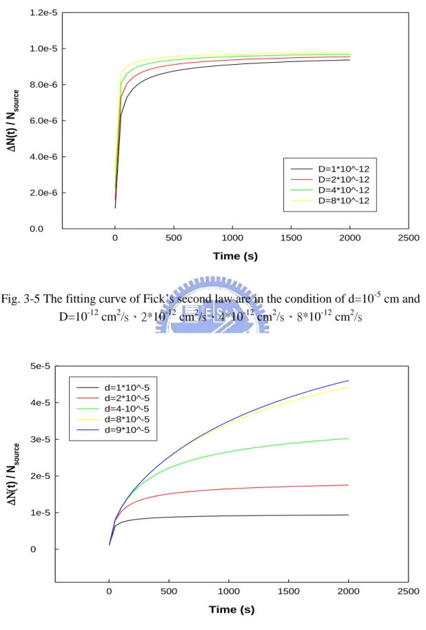
3-1.3 Gas diffusion model
Oana et al. [31] used Fick‘s second law to model the one dimension diffusion of
gases into pentacene single crystals. The total quantity of gas molecules in pentacene
crystal is obtained by integrating Fick‘s second law over the length of the diffusion
pentacene. An extra term needs to be added in the solution (Nstart). This term reflects
the fact that the measurement starts at t=0 with a quantity of gas that was accumulated
in crystal. The equation of modeling the diffusion of gases in pentacene is thus:
(3-1)
where N(t) is the molar fraction of gas at time t, Nsource is the gas flow expressed as
molar fraction, d is the length of the crystal in the direction in which the one
dimension diffusion occurs, and D is the diffusion coefficient. Their result showed the
diffusion length is similar to the pentacene film thickness.
We rewrite the equation (3-1) to another form:
(3-2)
Δ N(t) represents the variation of gas in pentacene film in time = t and is expressed as molar fraction. We tried to simulate the relations between equation (3-2) and
diffusion coefficient (D)、diffusion length (d) by Matlab . In Fig.3-5, we set
diffusion length d as 1000 Ǻ and varied the value of diffusion coefficient D. As the
2 start source source N(t)-N ( ) 2 { [1 ( )] [1 exp( )]} N N 2 4 N t d d d erf Dt Dt Dt 2 start 2 N(t)=N N { [1 ( )] [1 exp( )]} 4 2 source d d d erf Dt Dt Dt
In other words, the response became faster. In Fig.3-6, we fixed the diffusion
coefficient D as 10-12 cm2/s and changed the diffusion length d. When the diffusion
length increased, the amount of gas that diffused into the pentacene film became
larger. From these results, we found if that the value of D/d was larger, the responses
of equation (3-2) became faster.
3-1.4 Gas concentration effect
The above all discussion about the gas sensing phenomenon was with a fixed
amount of ammonia concentration. In Fig.3-7, we added different amount of
ammonia and observed the threshold voltage shifts. When the amount of ammonia
increased, the threshold voltage shift also increased. To study the gas sensing
mechanism in different ammonia concentration, we used the Fick‘s second law to fit
the experiment results in Fig.3-8. An agreement can be found when the following
relationship is proposed.
(3-3)
In this relationship, we assumed that the threshold voltage shift was due to the extra
charge that came from the gas molecules.K is the ratio of molecules which form the
effective charge. ( ) ox th source N t C V K N
In Fig.3-8, we set diffusion length d as 10-5cm and varied the fitting
parameter D、K to obtain the simulation result. In the condition with 2ℓ ammonia, D is 1.5*10-13 cm2/s and K is 4.93*10-13. But in 10ℓ ammonia condition, the fitting parameters are D= 5*10-13 cm2/s and K=5.31*10-13. The
increase of ammonia concentration increased the diffusion coefficient ―D‖ and
enhanced the percentage of ammonia molecules which can induce the threshold
voltage shift.
3-1.5 The phenomenon of different NH
3exposed time
In previous experiments, Fick‘s second law can successfully explain that the
ammonia enhanced the threshold voltage shift. But we observed another interesting
phenomenon in the ammonia-OTFT sensor.
We measured three identical devices that were placed at the same distance from
the cotton mass. When the measurement was applied on the three devices one after
another along with the NH3 sensing time, the threshold voltage variations of these
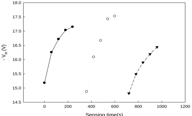
three devices were depicted in Fig.3-9. Interestingly, these three devices had similar
initial threshold voltages no matter how long these devices had been exposed to the
3-2 The phenomenon of bias stress gas sensing
In section 3-1.5, we observed that bias seem to play a critical role in gas
sensing. In this section we looked forward to verifying the relationship between gas
sensing and bias-stress effect
3-2.1 The theory of bias stress effect
At first, we introduce the theory of bias stress effect [32]. Bias stress effect
means applying a prolonged bias to the gate electrode and causes the threshold
voltage shifts by creating new electronic states or defects. For a-Si TFTs two major
models were developed to explain Vth shifts. [33.34] Although, the underlying
microscopic processes are different, in both models the creation of states is governed
by a dispersive process. In these models, the density of states, ∆ND, is proportional to
∆Vth, since ∆ND=Cox∆Vth. These states are the ones that must be filled before
significant conduction can occur via accumulation layer. Thus, the more defects
created during bias stress, the more holes are needed to occupy these defect states,
resulting in a threshold voltage shift. In other words, the driving force for defect
creation is charge trapping into defect-creation sites. Therefore, the rate at which
defects are created depends on the density of free holes induced by the gate bias. In
by charged defects. Based on these models it is readily shown that the rate of change
in Vth is given by differential equation [35.36]:
1 0 ( ( ) th D BT dV d N t N t dt dt t (3-4)
where NBT (t) represents the concentration of free holes in the accumulation channel.
Solving equation (3-4) with α=1 yields the stretched exponential function as given:
( ) 1 exp th th th ini ini G th t V V V V V (3-5) where ini th
V is the initial threshold voltage. is a dispersion parameter that can be
extracted by plotting log
ln
1VT/(VGVTini)
as a function of log(t) and represents the effective trapping time that can be expressed by
1 exp(E ) kT
(3-6)and can be obtained by measuring the stretched exponential curves at different
temperatures. According to equation (3-6), in a plot of the form log (τ) as a function
of 1/T, the slope of this curve represents the activation energy for defect creation,
Eτ=Ea/β . In other words, the value of Eτ, is a measure of the device stability.
3-2.2
The phenomenon of bias stress gas sensing
In order to study the phenomenon of bias stress gas sensing in detail, we
designed the following experiments:
Firstly, we measured the devices with bias stress of -7V、-11V、-15V. The
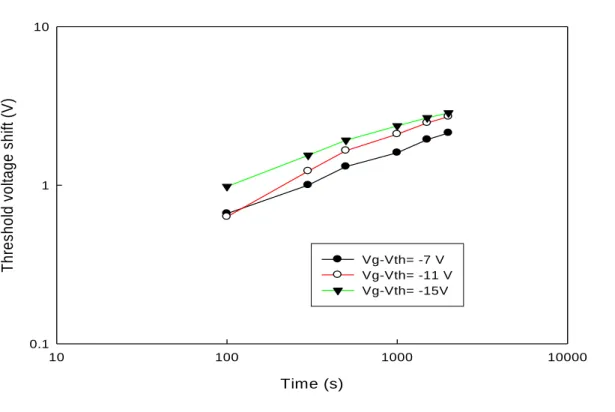
results are shown in Fig.3-10. When the gate bias was increased, the threshold voltage
shift was also increased. Then, we used the log scale to illustrate the experiment result
as shown in Fig.3-11. It is found that the threshold voltage has a power law
dependence on time. In other words, the experiment result is the same with the theory
of bias stress effect.
Next we measured four identical devices with different amount of ammonia
under -7V gate bias stress. We supposed that if the gate bias stress is the most
important factor in the sensing mechanism, no matter how much ammonia we added,
the threshold voltage shifts are all the same. In Fig.3-12, although we stressed bias in
Maybe the gate bias stress and the ammonia concentration all play critical roles in the
gas sensing behavior.
Then, in Fig.3-13, 3-14 we used amounts of ammonia concentration under
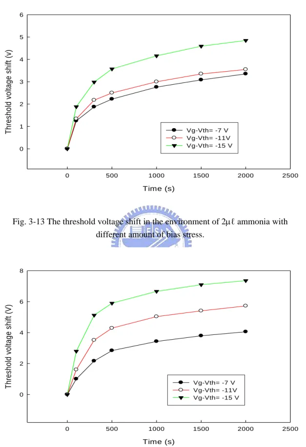
different stressed biases. In Fig.3-13 and 3-14 we added 2ℓ and10ℓ ammonia,
respectively. In the same ammonia environment, the threshold voltage shift increased
when the bias stress was increased. Comparing Fig.3-13 with Fig.3-14, 10ℓ
ammonia enhanced more threshold voltage shifts than 2ℓ under the same condition
of gate bias stress.
Actually the bias stress effect also caused the threshold voltage shifts in the
above experiment. But we look forward to studying the mechanism only between gas
concentration and gate bias stress. Therefore, we subtracted the bias stress effect in
Fig.3-10 from the experiment data of Fig.3-14 and showed the result in Fig. 3-15. In
Fig. 3-15, the simulation formula comes from the equation (3-3). The fitting
parameters are shown in Fig. 3-15. When the stressing bias is increased, the diffusion
coefficient increased. The diffusion behavior became more obvious. At the same time,
3-2.3 The gas sensing mechanism under bias stress
From the above experiment, we proposed two kinds of gas sensing mechanism
under bias stress.
3-2.3.1 Charge- trapped states
We considered the NH3 molecules are absorbed onto the surface of active
material or absorbed into the film through diffusion. The absorptive behavior between
NH3 molecules and pentacene molecules could result in charge-trapped state in
pentacene film. Therefore we observed the threshold voltage shift in the environment
with ammonia gas. When we increased the concentration of ammonia, the diffusion
became more obvious. Much more ammonia molecules can react with pentacene and
enhanced the variations of threshold voltage.
3-2.3.2 Dipole molecules
In the beginning, the ammonia is absorbed onto the surface of active material.
Then the ammonia molecules diffuse into the pentacene film through the grain
boundary. Because ammonia is a dipole molecule, bias stress can enhance the NH3
molecule to absorb onto the surface of pentacene or diffused into the film. Moreover
pentacene-based OTFT is a p-type transistor. We need to bias negative voltage for
accumulation. In this condition, the ammonia molecules diffuse into the active layer
have to apply much more negative bias to overcome the ammonia-induced electronic
Chapter 4
Conclusion
In this study we showed that the NH3 molecules are absorbed onto the surface
of active material and diffuse into the film. The absorptive behavior between NH3
molecules and pentacene molecules result in the variation of threshold voltage. The
threshold voltage shift may originate from creating charge-trapped states of
pentacene and polar molecules – ammonia.
Fick‘s second law can successfully explain the variations of threshold voltage in
the present of ammonia. When the concentrations of NH3 increase, the diffusion
coefficient increase and much more ammonia molecules contribute to the threshold
voltage shift. But we also observed that three identical devices had similar initial
threshold voltages no matter how long these devices had been exposed to the NH3
gas. This result implied that the sensing behavior may have a strong correlation with
the gate bias.
In addition, we varied the value of bias stress and fixed ammonia concentration.
In order to reduce the threshold voltage shifts resulting from the bias stress effect,
we subtracted the bias stress effect from the experimental data. Then, we observed
that the bias stress increase enhanced the variation in the threshold voltage. At the
Finally, we propose that gas diffusion and gate bias both play critical roles in
Reference
[1]. M. Pope and C.E. Swenberg, Electronic Processes in Organic Crystals and polymer,Oxford University Press, New York, 1999.
[2]. D.F. Barbe and C.R. Westgate ‖Surface state parameters of metal-free phthalocyanine single crystals‖. J. Phys. Chem. Solids ,31, 2679 (1970).
[3]. M.L. Petrova and L.D. Rozenshtein ‖Field effect in the organic semiconductor‖ Chloranil Fiz. Tverd. Tela, Soviet Phys. Solid State, 12, 961 (1970).
[4]. M.L. Petrova and L.D. Rozenshtein:‖Field effect in the organic semiconductor chloranil. Fiz. Tverd. Tela ,Soviet Phys. Solid State, 12, 961 (1970).
[5]. F. Ebisawa, T. Kurokawa, and S. Nara,‖Electrical properties of polyacetylene-polysiloxane interface‖, J. Appl. Phys, 54, 3255 (1983). [6]. A. Tsumura, K. Koezuka, and T. Ando‖ Macromolecular electronic device:
Field-effect transistor with a polythiophene thin film‖, Appl. Phys. Lett.,49, 1210 (1986).
[7]. Björn Timmer, Wouter Olthuis and Albert van den Berg,‖ Ammonia sensors and their applications—a review‖, Sensors and Actuators B, 107, 666 (2005)
[8]. M. Wallin, C-J. Karlsson, M. Skoglundh,‖ Selective catalytic reduction of NOx with NH3 over zeolite H-ZSM-5: influence of transient ammonia supply‖, J.
Catal.,218, 354
[9]. X. Xuan, C. Yue, S. Li,‖ Selective catalytic reduction of NO by ammonia with fly ash catalyst‖, Fuel 82, 575 (2003).
[10].Steven G. Buckley, Christopher J. Damm, Wolfgang M. Vitovec,‖ Ammonia Detection and Monitoring with Photofragmentation Fluorescence‖, Applied Optics, 37, 8382 (1998)
[11]. L.R. Narasimhan, W. Goodman, C. Kumar,‖ Correlation of breath ammonia with blood urea nitrogen and creatine during hemodialysis‖, PNAS, 98, 4617 (2001)
[12]. D.J. Kearney, T. Hubbard, D. Putnam,‖ Breath ammonia measurement in Helicobacter pylori infection‖, Digest. Dis. Sci, 47, 2523 (2002)
[13].N.K. Jain, V. Mangal, ―Helicobactor pyroli infection in children‖, J. Nep. Med. Assoc, 38, 140 (1999)
[14]. K. Zakrzewska, ―Mixed oxides as gas sensors‖, Thin Solid Films, 391, 229 (2001)
[15].N. Yamazoe, ―Chemical Sensor Technology‖, Elsevier, Amsterdam, 1991. [16]. X. Wang, N. Miura, N. Yamazoe, ―Study of WO3-based sensing material for
NH3 and NO detection‖, Sens. Actuators B ,66, 74 (2000).
[17]. C.N. Xu, N. Miura, Y. Ishida, ―Selective detection of NH3 over NO in
combustion exhausts by using Au and MoO3 doubly promoted WO3 element‖,
Sens. Actuators B, 65163 (2000)
[18]. V.V. Chabukswar, S. Pethkar, A.A. Athawale‖, Acrylic acid doped polyaniline as an ammonia sensor‖, Sens. Actuators B , 77 657 (2001)
[19]. L. Torsi, A. Dodabalapur, L. Sabbatini, P.G. Zambonin, ―Multi-parameter gas sensors based on organic thin-film-transistors‖ Sensors and Actuators B, 67, 312, (2000).
[20]. F. Liao, C. Chen, V. Subramanian, ―Organic TFTs as gas sensors for electronic nose applications,‖ Sensors and Actuators B, 17, 849 (2005).
[21]. M.C. Tanese, D. Fine, A. Dodabalapur, L. Torsi, ―Interface and gate bias dependence responses of sensing organic thin-film transistors,‖ Biosensors and
[22]. B. Crone, A. Dodabalapur, A. Gelperin, L. Torsi, H. E. Katz, A. J. Lovinger, and Z. Bao ―Electronic sensing of vapors with organic transistors,‖ Appl. Phys. Lett.,
78, 3965, (2001).
[23]. L. Torsi, M.C. Tanese, N. Cioffia, M.C. Gallazzi,L. Sabbatini, and P.G. Zambonin, ―Alkoxysubstituted polyterthiophene thin-film-transistors as alcohol sensors,‖ Sensors and Actuators B, 98, 204,(2004)
[24]. B. Crone, A. Dodabalapur, A. Gelperin,‖ Electronic sensing of vapors with organic transistors‖ Appl Phys Lett 78, 2229, (2001)
[25] JB Chang,‖Functionalized Polythiophene Thin-film Transistors for Low-cost Gas Sensor Arrays‖,eecs.berkeley.edu, 2006
[26].Torsi L, Lovinger AJ, Crone B, ―Correlation between Oligothiophene Thin Film Transistor Mophology and Vapor Response‖, J Phys Chem B, 106, 12563 (2002)
[27]. Liang Wang, Daniel Fine, and Ananth Dodabalapur,‖ Nanoscale chemical sensor based on organic thin-film transistors‖, Appl. Phys. Lett., 85, 6386, 2004. [28]. C. D. Dimitrakopoulos, A. R. Brown, and A. Pomp, ―Molecular beam deposited
thin films of pentacene for organic field effect transistor applications‖, J. Appl. Phys.,80, 2501, (1996)
[29]. Chih-Wei Chu, Sheng-Han Li, Chieh-Wei Chen,―High-performance organic thin-film transistors with metal oxide/metal bilayer electrode‖, Appl. Phys. Lett., 87, 193508, (2005).
[30]. A.Alec Talin, Luke L. Hunter, François Léonard,‖ Large area, dense silicon nanowire array chemical sensors‖ , Appl. Phys. Lett. 89, 153102 (2006)
[31].Oana D. Jurchescu, Jacob Baas, and Thomas T. M. Palstra,‖ Electronic transport properties of pentacene single crystals upon exposure to air‖, Appl. Phys. Lett. 87, 052102 ,(2005)
[32].Henrique L. Gomes, Peter Stallinga, Franco Dinelli, ―Electrical characterization of organic based transistors: stability issues‖,Polym.Adv. Technol.16, 227,(2005).
[33]. Jackson WB, Marshall JM,‖ Role of hydrogen in the formation of metastable defects in hydrogenated amorphous silicon” Phys. Rev. B ,39,1164 (1989) [34]. Crandall RS.‖ Defect relaxation in amorphous silicon: Stretched
exponentials, the Meyer-Neldel rule, and the Staebler-Wronski effect” Phys Rev. B, 43,4057 (1991)
[35]. Wehrspohn RB, Deane SC, French ID, ―Relative importance of the Si–Si bond and Si–H bond for the stability of amorphous silicon thin film transistors.‖ J. Appl. Phys.,87, 144 (1999).
[36]. Wehrspohn RB, Deane SC, French ID, ―Effect of amorphous silicon material properties on the stability of thin film transistors: evidence for a local defect creation model ‗J. Non-Cryst. Solids, 266, 459(2000)
Fig. 1-1 Molecular structure of pentacene.
Fig. 1-2 (a) Top contact structure.
Fig. 1-3 The work function of various metals and ionization potential of pentacene.
wet oxide(100nm)
Heavily doped Si substrate
Pentacene (100nm)
Au(100nm)
0.0 1.0x10⁻⁶ 2.0x10⁻⁶ 3.0x10⁻⁶ 4.0x10⁻⁶ 5.0x10⁻⁶ 6.0x10⁻⁶ 10-12 10-11 10-10 10-9 10-8 10-7 10-6 10-5 10-4 -40 -30 -20 -10 0 10 0.0 5.0x10⁻⁸ 1.0x10⁻⁷ 1.5x10⁻⁷ 2.0x10⁻⁷ 2.5x10⁻⁷ I D (A ) VG(V) I D (A ) G M pure device with 2ml NH3 60s with 2ml NH3 120s with 2ml NH 3 180s with 2ml NH 3 240s with 2ml NH3 300s -18 -17 -16 -15 -14 -13 1.00 1.25 1.50 0 50 100 150 200 250 300 0.55 0.60 0.65 Vth (V ) T i m e ( s ) S .S(V/de ca d e) m o b ilit y (cm 2 /Vs) 0.021 3.35 -18 -17 -16 -15 -14 -13 1.00 1.25 1.50 0 50 100 150 200 250 300 0.55 0.60 0.65 Vth (V ) T i m e ( s ) S .S(V/de ca d e) m o b ilit y (cm 2 /Vs) 0.021 3.35
Fig. 3-1 The electrical properties of OTFT adding 2ℓ NH3.
Fig. 3-2 The variations of subthreshold swing、threshold voltage and mobility along with time in environment of 2ℓ NH3 (after pink line).
Fig. 3-3 The variations of threshold voltage along with time in environment of 2ℓ NH3 Time (s) 0 2000 4000 6000 8000 10000 12000 14000 -V th ( V ) 16 18 20 22 24 26 28
initial
Add 20
ℓ NH
3Remove
NH
3 Time(s) 0 50 100 150 200 250 300 350 -V th (V ) 13.5 14.0 14.5 15.0 15.5 16.0 16.5 17.0 17.5Add 2
ℓ NH
3Time (s) 0 500 1000 1500 2000 2500 N(t) / N so ur ce 0.0 2.0e-6 4.0e-6 6.0e-6 8.0e-6 1.0e-5 1.2e-5 D=1*10^-12 D=2*10^-12 D=4*10^-12 D=8*10^-12
Fig. 3-5 The fitting curve of Fick‘s second law are in the condition of d=10-5 cm and D=10-12 cm2/s、2*10-12 cm2/s、4*10-12 cm2/s、8*10-12 cm2/s Time (s) 0 500 1000 1500 2000 2500 t) / Nso ur ce 0 1e-5 2e-5 3e-5 4e-5 5e-5 d=1*10^-5 d=2*10^-5 d=4-10^-5 d=8*10^-5 d=9*10^-5
Fig. 3-6 The fitting curve of Fick‘s second law are in the condition of D=10-12 cm2/s
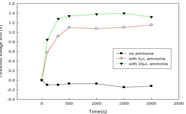
Fig. 3-7 The threshold voltage shift in different amount of NH3.
Fig.3-8
Fig. 3-8 The dependence of threshold voltage shift on sensing time in the
Time(s) 0 500 1000 1500 2000 2500 T h re sh o ld v o lta g e s h ift ( V ) -0.4 -0.2 0.0 0.2 0.4 0.6 0.8 1.0 1.2 1.4 1.6 no ammonia with 2L ammonia with 10L ammonia Time (s) 0 500 1000 1500 2000 2500 T h re s h ld v o lt a g e s h if t (V ) 0.0 0.2 0.4 0.6 0.8 1.0 1.2 1.4 1.6
experiment result ( 2ul NH3 ) experiment result ( 10ul NH3 ) simulation result ( 2ul NH3 ) simulation result ( 10ul NH3 ) D=5*10-13 cm2/s, K=5.31*10-13
Fig. 3-9 The threshold voltage variation of three identical devices measured one after another in the environment with NH3 gas. The NH3 amount
injected into the cotton mass was 2ℓ.
Fig. 3-10 The threshold voltage shift in different bias stress conditions
Sensing time(s) 0 200 400 600 800 1000 1200 - V th (V ) 14.5 15.0 15.5 16.0 16.5 17.0 17.5 18.0 Time (s) 0 500 1000 1500 2000 2500 T h re s h o ld v o lt a g e s h if t (V ) 0.0 0.5 1.0 1.5 2.0 2.5 3.0 Vg-Vth= -7 V Vg-Vth= -11 V Vg-Vth= -15V
Fig. 3-11 The threshold voltage shift in different bias stress conditions
Fig. 3-12 The threshold voltage shift in different amount of concentrations with
Time (s) 10 100 1000 10000 T h re sh o ld v o lta g e s h ift ( V ) 0.1 1 10 Vg-Vth= -7 V Vg-Vth= -11 V Vg-Vth= -15V Time(s) 0 500 1000 1500 2000 2500 T h re sh o ld v o lta g e s h ift ( V ) 0.0 0.5 1.0 1.5 2.0 2.5 3.0 3.5 pure device with 2ul NH3 with 10ul NH3 with 20ul NH3
Fig. 3-13 The threshold voltage shift in the environment of 2ℓ ammonia with different amount of bias stress.
Fig. 3-14 The threshold voltage shift in the environment of 10ℓ ammonia with different amount of bias stress.
Time (s) 0 500 1000 1500 2000 2500 T h re sh o ld v o lta g e s h ift ( v) 0 1 2 3 4 5 6 Vg-Vth= -7 V Vg-Vth= -11V Vg-Vth= -15 V Time (s) 0 500 1000 1500 2000 2500 T h re sh o ld v o lta g e s h ift ( V ) 0 2 4 6 8 Vg-Vth= -7 V Vg-Vth= -11V Vg-Vth= -15 V
Fig. 3-15 The dependence of threshold voltage shift on sensing time in the environments with different gate bias strees. The circles are experiment data. The curves are the fitting result from Fick‘s second law.
Time (s) 0 500 1000 1500 2000 2500 T hre sho ld v ol tag e shi ft (V ) 0 1 2 3 4 5 Vg-Vt = -7V Vg-Vt = -11V Vg-Vt = -15V simulation result simulation result simulation result D=1.7*10-13 cm2/s, K=1.82*10-2 D=1.1*10-13 cm2/s, K=1.38*10-2 D=0.5*10-13 cm2/s, K=0.983*10-2