國 立 交 通 大 學
電機學院與資訊學院 電子與光電學程
碩
士
論
文
利用環型震盪器探討元件變異對
低溫多晶矽薄膜電晶體電路效能之研究
研 究 生:張富智
指導教授:戴亞翔 博士
中 華 民 國 九 十 五 年 六 月
利用環型震盪器探討元件變異對
低溫多晶矽薄膜電晶體電路效能之研究
研 究 生:張富智 Student:Fu-Chi Chang
指導教授:戴亞翔 Advisor:Ya-Hsiang Tai
國 立 交 通 大 學
電機學院與資訊學院專班 電子與光電學程
碩 士 論 文
A ThesisSubmitted to Degree Program of Electrical Engineering and Computer Science College of Electrical and Computer Engineering
National Chiao Tung University in partial Fulfillment of the Requirements
for the Degree of Master of Science
in
Electronics and Electro-Optical Engineering June 2006
Hsinchu, Taiwan, Republic of China
利用環型震盪器探討元件變異對
低溫多晶矽薄膜電晶體電路效能之研究
研究生: 張富智 指導教授: 戴亞翔博士
國立交通大學
摘 要
低溫多晶矽薄膜電晶體(LTPS TFT)最近幾年在液晶顯示器(AMLCD)應用中之所 以會是眾所注目的焦點,是因為其優異的元件特性。然而,由於複晶矽層不規則的晶粒 邊界分佈,低溫多晶矽薄膜電晶體有較差的均勻性,同時元件參數呈現大範圍變動。元 件 變 異 的 來 源 可 由 其 元 件 分 佈 的 距 離 來 區 分 為 宏 觀 (macroscopic) 及 微 觀 (microscopic)兩類。 本論文主要是探討低溫多晶矽薄膜電晶體的元件特性變動問題對數位電路效能的影 響。在探討微觀元件變異的效應上,我們可以預測其變異的範圍並且更進一步的在模擬 及量測間得到一致的結論。在探討宏觀元件變異的效應上,我們說明一個新的觀念來評 估宏觀元件變異對電路效能的影響。同時,我們也藉由比較是否考慮微觀元件變異來驗 證它對電路效能的影響將會呈現平均化。總結上面分析的結果,我們可以提出一套有效 率的模擬方法來考量複晶矽薄膜電晶體的元件變異性以獲得高良率的低溫多晶矽薄膜 電晶體數位電路。Study on the Device Variation Effect on LTPS TFT
Circuit Performance Using Ring Oscillator
Student:
Fu-Ji
Chang
Advisor:
Dr.Ya-Hsiang
Tai
Chiao Tung University
Abstract
Low temperature poly-silicon silicon (LTPS) thin film transistors (TFTs) have recently attracted much attention in the application on the integrated peripheral circuits of active matrix liquid crystal displays (AMLCDs). However, due to the irregularly distributed grain boundary, LTPS TFTs have poor uniformity and suffer from huge variation. Device variation sources can be divided into micro variations characterized by short correlation distances and macro variations characterized by long correlation distances.
The thesis studies the issues about the device characteristic variation of LTPS TFT affecting on the digital logic circuit performance. On the microscopic device variation aspect, we predict its variation range and the consistence between measurement and simulation results are also presented. On the macroscopic device variation aspect, we demonstrate a new concept on how to simulate macroscopic device variation effect on LTPS TFT circuit performance. Meanwhile, the microscopic device variation effect on circuit performance is evaluated to be as averaged type by doing the comparison between with and without it. With these analysis results, we can provide efficient methods to characterize and model circuit variation to obtain high-yield LTPS TFT digital circuits.
誌 謝
在短暫的兩年研究所生涯中,感謝我能如此幸運,有一個如此完善的研
究環境。首先要感謝的,便是我的指導教授戴亞翔博士。由於老師的細心
引導與仔細教導,使我能在研究上獲得些成果。除此之外,也感謝老師在
待人處世以及生涯規劃上帶給我的啟發,使我受益良多,有所成長。在這
裡要先對戴老師致上誠摯的謝意。
感謝這一條研究的路上,身邊有無數優秀的研究人才相伴。同時亦感謝
學長們的鼓勵與協助,讓我在實驗上感到迷惑時能順利找到研究的方向。
感謝這兩年來和我一起奮鬥同甘共苦的夥伴們,同實驗室的俊文、婉萍、
國烽及可青感謝你們花時間分享相關研究成果。
最後,我要感謝我的家人,總是在背後默默的支持我、給予我高度的肯
定並以我為傲,在此我要向他們送上最真摯的感謝。
僅以此文獻給我的老師、家人與好友。
富智2006
Table of Contents
ABSTRACT (Chinese)... i ABSTRACT (English)... ii ACKNOWLEDGEMENTS... iii TABLE OF CONTENTS………...iv LIST OF FIGURES………v LIST OF TABLES………viiChapter 1 Introduction and Motivation ………... 1
1.1 Why LTPS TFTs…...1
1.2 LTPS TFTs Device Variation...2
1.3 Simulation Method Review...3
1.3.1 Worst Case Method……….………….………... 3
1.3.2 Monte Carlo Method……….……….. . 4
1.4 Why Ring Oscillator ….…...4
1.5 Organization of Thesis………..5
Chapter 2 Device Variation ………... 9
2.1 Introduction to Crosstie TFTs... 9
2.2 LTPS TFTs Initial Parameter Distribution...10
2.3 The Distribution of Initial Parameter Difference with Different Device Distance...12
Chapter 3 Implementation of Ring Oscillator with LTPS TFTs ... 23
3.1 Device Fabrication... 23
3.2 Testkey Design and Layout………... 23
3.3 Measurement and Device Parameter Extraction Method ...24
3.3.1 Measurement Method………..………. ...24
3.3.2 Parameter Extraction……….………...25
3.4 Results….……….26
Chapter 4 Device Variation Effects on Ring Oscillator……... 37
4.1 Microscopic Device Variation Effect on Ring Oscillator... 37
4.2 Macroscopic Device Variation Effect on Ring Oscillator... 39
4.3 Summary...43
Chapter 5 Conclusions and Future Works………... 50
List of Figures
Figure caption- Chapter 1
Fig. 1-1 The variation of the transfer characteristics of Id-Vg curve for LTPS TFTs…………7
Fig. 1-2 The variation of the transfer characteristics of Id-Vd curve for LTPS TFTs…………7
Fig. 1-3 The diagram of different TFTs with various amount of grain boundaries existing in the channel………...8
Fig. 1-4 Probability density function for (a) a Gaussian and (b) a uniform random…………..8
Figure caption- Chapter 2
Fig. 2-1 The layout of the crosstie TFTs………...15Fig. 2-2 The initial distribution of N-type TFT threshold voltage (Vth)………..15
Fig. 2-3 The initial distribution of N-type TFT mobility (Mu)……….15
Fig. 2-4 The initial distribution of P-type TFT threshold voltage (Vth)………...16
Fig. 2-5 The initial distribution of P-type TFT mobility (Mu)……….16
Fig. 2-6 A chart demonstrates device parameter distribution along distance corresponding to the concept of noise……….17
Fig. 2-7 A chart demonstrates device parameter distribution along distance corresponding to the concept of signal and noise ……….17
Fig. 2-8 The average and standard deviation of TFT threshold voltage (Vth) difference……18
Fig. 2-9 The average and standard deviation of TFT mobility (Mu) difference………..18
Fig. 2-10 The distribution of N-type TFT threshold voltage (Vth) difference……….19
Fig. 2-11 The distribution of P-type TFT threshold voltage (Vth) difference……….20
Fig. 2-12 The distribution of N-type TFT mobility (Mu) difference………...21
Fig. 2-13 The distribution of P-type TFT mobility (Mu) difference………22
Figure caption- Chapter 3
Fig. 3-1 The schematic cross-section structure of the n-type TFT………...30Fig. 3-2 The schematic cross-section structure of the p-type TFT………...30
Fig. 3-3 The schematic of ring oscillator test-key………30
Fig. 3-4 The layout picture of ring oscillator test-key………..31
Fig. 3-5 The layout picture of buffer block in ring oscillator test-key……….31
Fig. 3-6 The layout picture of probing pad block in ring oscillator test-key………32
Fig. 3-7 The block diagram of measurement method for ring oscillator test-key inverter delay time Td……….………...32
Fig. 3-8 The relationship between output frequency of three stages ring oscillator and inverter delay time Td………..33
Fig. 3-9 Switch model of dynamic behavior of static inverter………..33
Fig. 3-10 Ring oscillator delay time histogram chart………34
Fig. 3-12 the distribution chart of ring oscillator supply current and square of supply voltage………35 Fig. 3-13 the distribution chart for standard deviation of RO power and frequency…………35 Fig. 3-14 Ring oscillator delay time error bar chart………..36
Figure caption- Chapter 4
Fig. 4-1 Simulation result of microscopic device variation effect on ring oscillator when operation voltage is 5V………..44 Fig. 4-2 Simulation result of microscopic device variation effect on ring oscillator when
operation voltage is 10V………44 Fig. 4-3 Simulation result of microscopic device variation effect on ring oscillator when
operation voltage is 15V………45 Fig. 4-4 the measured microscopic device variation effect on delay time with respect to
operating voltage is 5V………..45 Fig. 4-5 the measured microscopic device variation effect on delay time with respect to operating voltage is 10V………46 Fig. 4-6 the measured microscopic device variation effect on delay time with respect to
operating voltage is 15V………46 Fig. 4-7 Histogram of an inverter circuit carries delay and its worst-case values………47 Fig. 4-8 the simulated delay time histogram of ring oscillator when operating voltage is 5V.
Device parameter combination is assumed to be random type, and the microscopic device variation effect is neglected………47 Fig. 4-9 the simulated delay time histogram of ring oscillator when operating voltage is 5V.
Device parameter combination is assumed to be random type, and the microscopic device variation effect is included………48 Fig. 4-10 Three types of combination between device parameters known as (N,N,P), random
and (P,P,N), respectively………48 Fig. 4-11 Error bar graph of measured and simulated delay time for 27 sets combination
between device parameters………..49 Fig. 4-12 the simulated delay time histogram of ring oscillator when operating voltage is 5V
List of Tables
Table2-1 The average values and standard deviation values of device parameters…………..11 Table4-1 PredictedΔMun, ΔVthn, ΔMup and ΔVthp at the 0.5% and 99.5% of the
distribution respectively……….………38 Table4-2 the measured device parameter average and standard deviation from the uniformly
Chapter 1
Introduction and Motivation
1-1. Why LTPS TFT
In recent years, with the flat-panel display technology development, flat-panel displays
have replaced the traditional cathode ray tube (CRT) application for many aspects. Liquid
crystal display (LCD) is one of the popular displays. Especially, thin film transistor liquid
crystal display (TFT-LCD) is the most common display at present. According to the
manufacture technique of thin film transistor (TFT), the TFT-LCD is categorized into
amorphous-silicon (a-Si) TFT and low-temperature poly-silicon (LTPS) TFT and high-
temperature poly-silicon (HTPS) TFT.
Among these TFTs, LTPS has been widely investigated as a material for mobile
applications such as digital cameras and note book computers. In polysilicon film, the carrier
mobility larger than 10 cm2/Vs can be easily achieved, that is about 100 times larger than that
of the conventional a-Si TFTs and fast enough to make peripheral driving circuit including n-
and p-channel devices. This enables the monotheistic fabrication of peripheral circuit and
TFT array on the same glass substrate, bringing the era of system-on-glass (SOG) technology
[1]. They also have been applied into some memory devices such as dynamic random access
only memories (EPROMs), electrical erasable programming read only memories
(EEPROMs), linear image sensors, thermal printer heads, photo-detector amplifier, scanner,
neutral networks. In the future, the application fields of LTPS TFTs will not be limited to
displays but will be expanded to other electronic devices, such as LSIs, printers andsensors.
1-2. LTPS TFTs Variation
The LTPS TFTs suffer from bad uniformity. The poly-Si material is a heterogeneous
material made of very small crystals of silicon atoms in contact with each other constituting a
solid phase material. These small crystals are called crystallites or grains. The presence of
these crystallites that have any type of orientation means a break in the crystal from one
crystallite to the other. Because the material remains solid, the atoms at the border of a
crystallite are also linked to the neighbor crystallite ones. However, these atom bonds are
disoriented in comparison with a perfect lattice of silicon. This border is called a grain
boundary. Owing to the existence of grain boundary, the variation of poly-Si TFT is intrinsic.
Currently, the formation of the crystallites in polysilicon is achieved by solid phase
crystallization (SPC), excimer laser crystallization (ELA), or metal-induced lateral
crystallization (MILC). None of the methods can control the growth of grain to be identical.
Due to the variety of the grain boundary, each TFT has different trap states distribution in the
Thus, the TFT characteristics can be distinguished even fabricated with the same process
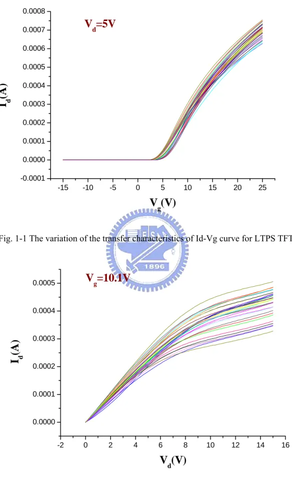
and LTPS TFTs always have different characteristic. Figure 1-1 shows the variation of the
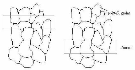
transfer characteristics of Id-Vg curve and Figure 1-2 shows the variation of the transfer
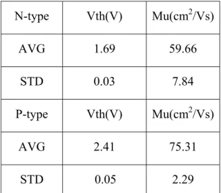
characteristics of Id-Vd curve. Figure 1-3 shows the different TFTs with various amounts of
grain boundaries existing in the channel. The disadvantage of the variation for LTPS TFTs
must be investigated.
1-3. Simulation Method Review
There are two major methods of simulation to analyze circuit performance, which are the worst-case and Monte Carlo analysis as described below.
1-3-1. Worst-Case Method [2]
Worst-case analysis is the most commonly used technique in industry for considering manufacturing process tolerances in the design of integrated circuits. These approaches are relatively inexpensive compared to the yield maximization approaches in terms of computational cost and designer effort, and they also provide high parametric yields. At any design point, uncontrollable fluctuations in the circuit parameters cause circuit performance to device from their nominal design values. The goal of worst case analysis is to determine the worst values that the performance may have under these statistical fluctuation. In addition to finding the worst-case values of the circuit performance, this analysis also finds the corresponding worst-case values of noise parameters. A noise parameter is treated as a random variable. Any random variable is characterized by probability density function (and by a mean and a standard deviation which depends on the density function), as shown in Fig. 1-4. The worst-case noise parameter vector is used in circuit simulation to verify whether
circuit performances are acceptable under these conditions. Similar to worst-case analysis, one can also perform best-case analysis. In fact, industrial designs are often simulated under best, worst, and nominal noise parameter conditions, which provide designers with quick estimates of range of variation of circuit performances.
1-3-2. Monte Carlo Method
Yield, expressed as a multi-dimensional integral, can be evaluated numerically using either the quadrature-based, or Monte Carlo based methods. The quadrature-based methods have computational costs that explode exponentially with the dimensionality of the statistical space. Monte Carlo methods, on the other hand, are less sensitive to the dimensionality. The Monte Carlo method is a computer simulation of real distributions of random noise parameters, and it is the simplest, most reliable and accurate of all methods used in practice. However, for high accuracy it requires a large number of sample points. Typically, hundreds of trials are required to obtain reasonable accurate yield estimation. For nonlinear and/or time domain circuit analysis, this is computational expensive. Hence, a fundamental problem to solve is to increase the efficiency of the Monte Carlo method and its accuracy, measured by the variance of the yield estimation.
1-4. Why Ring Oscillator
The previous sections have noted the importance of the knowledge of LTPS TFT device variations. By obtaining a better understanding of these variation sources and how they are correlated with other physical parameters, variation models can be developed which would be beneficial not only for optimal circuit performance, but for the assurance of the circuit’s functionality. Therefore, experiments and tests first have to be conducted on the process to provide useful data that would lead to the better knowledge of these variation sources.
measure variation within a LTPS TFT process. A ring oscillator test key is therefore implemented containing numerous test structures that can correlate certain device variations. The ring oscillator is chosen out here owing to its output frequency not only can be made sensitive to device parameter but also a direct circuit-level timing parameter that can be easily measured. Besides, it deserves to be mentioned that standard CMOS digital logic circuit performance can be generalized relatively effectively by ring oscillator (RO) frequency. By measuring the frequencies at which these test structures oscillate, valuable information can be obtained that can effectively characterize device variation in a given process.
The use of ring oscillators to detect variation is not a new concept. The unique contribution of this thesis is to compare the difference between real circuit and simulation with measurement and statistical analysis. Then we can verify efficient methods to characterize and model circuit variation to obtain high-yield poly-Si TFTs digital circuits.
1-5. Organization of Thesis
Chapter 1. Introduction and Motivation for Research 1-1. Why LTPS TFTs
1-2. LTPS TFTs Device Variation 1-3. Simulation Method Review
1-3-1 Worst Case Method 1-3-2 Monte Carlo Method 1-4. Why Ring Oscillator 1-5. Organization of Thesis Chapter 2. Device Variation
2-1. Introduction to Crosstie TFTs
2-2. LTPS TFTs Initial Parameter Distribution
Chapter 3. Implementation of Ring Oscillator with LTPS TFTs 3-1. Device Fabrication
3-2. Testkey Design and Layout
3-3. Measurement and Device Parameter Extraction Method 3-3-1 Measurement Method
3-3-2 Parameter Extraction 3-4. Results
Chapter 4. Device Variation Effects on Ring Oscillator
4-1. Microscopic Device Variation Effect on Ring Oscillator 4-2. Macroscopic Device Variation Effect on Ring Oscillator 4-3. Summary
-15 -10 -5 0 5 10 15 20 25 -0.0001 0.0000 0.0001 0.0002 0.0003 0.0004 0.0005 0.0006 0.0007 0.0008
V
d=5V
I
d(A)
V
g(V)
Fig. 1-1 The variation of the transfer characteristics of Id-Vg curve for LTPS TFTs.
-2 0 2 4 6 8 10 12 14 16 0.0000 0.0001 0.0002 0.0003 0.0004 0.0005
V
g=10.1V
I
d(A)
V
d(V)
Fig. 1-3 The diagram of different TFTs with various amount of grain boundaries existing in the channel.
Chapter 2
Device Variation
2-1. Introduction to Crosstie TFTs
In previous studies, it is known that LTPS TFTs are found to suffer serious device variation even under well-controlled process. Since device variation will directly affect the circuit performance and reliability prediction, it is essential to understand where the variation may come and how the behavior variation could be. Due to the low process temperature, LTPS TFTs have different processes from IC industry. Besides, LTPS TFTs have less controllable defect number and distribution in the channel film. These may be the sources of device variation. In MOSFETs (Metal Oxide Semiconductor Field Effect Transistors), device variation sources can be divided into micro variations characterized by short correlation distances and macro variations characterized by long correlation distances, where the correlation distance is defined as the distance in which a process disturbance affects the device performance. Generally, the behaviors of the macroscopic and microscopic variation are the common and random variation, respectively. On the other hand, from the varying phenomena we can understand what variation type was occurred in the devices. Usually, macro variations come from the issues of process control, including gate insulator thickness lightly doped drain (LDD) length fluctuation and ion implantation uniformity; micro variations come from the difference of the defect site, defect density in the active region and the activation efficiency. If this correlation distance is lower than the distance between devices, the disturbance constitutes micro variations and affects few devices (e.g. a charge trapped in the gate oxide layer). On the other hand if this distance is longer than mutual device distance, the disturbance composed of micro variations and macro variations affects all the devices within a defined region. Therefore, the devices placed at longer distance suffer
more serious variation than devices placed close to each other.
In order to study the relationship between uniformity issue and device distance, a special layout of the devices adopted in this work is shown in Fig 2-1. The structure of the poly-Si film and the gate metal are in the order that resembles the crosstie of the railroad and therefore this layout is called the crosstie type layout of LTPS TFTs. The distance of mutual device is equally-spaced 40µm. In this small distance, the macro variation may be ignored and the variation of device behavior can therefore be reduced to only micro variation. So we can find out the relationship between the variation behaviors and the distance of mutual device by adopting the crosstie layout TFTs.
2-2. LTPS TFTs Initial Parameter Distribution
Before the following analysis, we introduce the statistical expressions, average value and standard variation. The average value AVG , X , is defined as
n i = 1 x X = n
∑
where x is the observe value. (2-1)
The standard deviation value STD, σ, is usually used to investigate the distribution of the observed value. The standard deviation value is given as
(
)
2 1 n x X n σ ≡∑
− (2-2)Where x is the observe value, X is the average value.
In order to obtain the more accurate parameter distributions of crosstie layout TFTs, large amount of TFT devices parameters are required. More than 1600 devices are measured and taken into statistical analysis in this work. The threshold voltage (Vth) and mobility (Mu) distributions of N-type TFT are shown respctively in Fig. 2-2 and Fig. 2-3 and those of P-type
are shown in Fig. 2-4 and Fig. 2-5. Table 2-1 is the average values and standard variation values of these initial parameter.
N-type Vth(V) Mu(cm2/Vs) AVG 1.69 59.66 STD 0.03 7.84 P-type Vth(V) Mu(cm2/Vs) AVG 2.41 75.31 STD 0.05 2.29
Table 2-1 The average values and standard deviation values of device parameters.
These figures show the variation behaviors in different parameters of LTPS TFTs. The Vth distrubtion of N-type TFT reveals the slight left-skewed property and the sharper peak compared with the Gaussian distribution. The Mu distribution of N-type TFT is apparently asymmetric and incisive in its peak. This phenomena indicates that field effect mobility exhibits severe non-uniformity behavior compared with threshold voltage. Then, the distribution S.S of N-type TFT follows the Gussian distribution. As for the Vth and Mu distributions of P-type TFT, both of them are similar to the Gussain distribution. The P-type TFT SS distribution shows two peak and asymmetric. In conclusions, some of these parameter distributions are diverse and cannot be explained. Although several studies have been made on the relationship between the grain boundaries in channel and threshold voltage and field effect mobility [3-6], there seems to be no well-established theory to explain. Therefore, if we want to find the variation behaviors with respect to the distance, it can not just classify them via these distributions and another grouping method should be mentioned. In the next section, it will get the more identical distributions, which will be more useful to
evaluate the variations in LTPS TFTs.
2-3. The Distribution of Initial Parameter Difference with Different
Device Distance
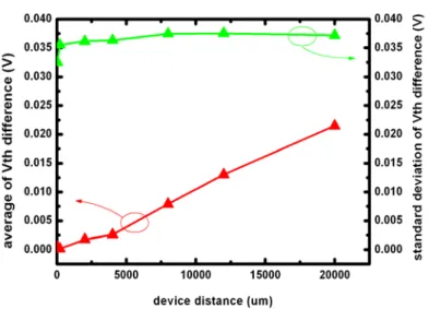
Fig. 2-6 illustrates the threshold voltage distribution along the device position. We can take this graph as a part of Fig. 2-7, which is the same kind of graph but in longer distance. Analogy to the small signal analysis in the circuit theory, the macro variation just likes the range near the bias point and appears in piecewise linear form, while the micro variation can be taken as the noise. In order to identify the effects of the macro and micro variation, the parameter differences of two devices under certain distance are divided with several groups according to the distance between two devices. In previous studies [7], the averages of parameters differences stand for macro variation of LTPS TFTs, while the standard deviation of parameter differences shows the micro variation in the devices. Fig. 2-8 and Fig. 2-9 show the average and the standard deviation of parameters differences of LTPS TFTs. As the mutual device distance increases, the deviations of these parameter differences almost do not change with the device distance. It can be explained that the micro variation will merely vary with distance as we expect. As for the macro variation, these figures show the diverse results. In the difference Vth, the average is increasing with device distance. However, the average of the Mu difference is decreasing when the distance of mutual devices is increasing. Although the averages of the differences of these parameters show different behaviors, they still appear in linear form. On the other hand, the effects of variation in a range are still minor than those of the micro variation under short device distance.
Since we know the device variation behaviors by above statistical analysis, how to apply these results to evaluate the effects of variation on the circuit performance is a topic we are interested in. Because the distance between two devices will not be too long for the layout
of the circuit, the macro variation is not our concern. A better approach is to find the proper mathematical expression for the distribution of the differences of these parameters. Firstly, we introduce the coefficient of determination (R square) to evaluate the fitness of our work, which is defined as 2 SSR 1 SSE r SST SST = = − , where 2 2 2 2 2 2 1 1 2 2 2 1 2 1 ˆ ˆ SSR=
∑
( y−y ) =∑
Y =b∑
X +b∑
X + b b∑
X X2 SST =∑
( y− y )2 SSE =∑
ˆe2 =∑
( yi−ˆy )i 2Generally speaking, the values of R square above 0.7 represnent the good fitness for the chosen funcion.
For the distribution of the difference of Vth, Gaussian-Lorentzian cross product is apply to the fitting, which is
(
)
2 2 - 1 1 *exp 1- * 2 a y x b x b d d c c = ⎛ ⎛ ⎞ ⎞ ⎛ ⎛ ⎞ + ⎜ ⎜ ⎟ ⎟ ⎜ ⎜ ⎟ ⎜ ⎝ ⎠ ⎟ ⎜ ⎝ ⎠ ⎝ ⎠ ⎝ - ⎞ ⎟⎟ ⎠ wherea is the peak value of the distribution b is the center of the distribution
c is fitting parameter related to the width of the distribution
d is fitting parameter varying from 0 to 1; 0 represents the pure Gaussain function ,while 1 is a pure Lorentzian distribution
Fig. 2-10 and Fig. 2-11 are shown respcetively the Vth difference distributions of N-type and P-type TFT with different device distance.
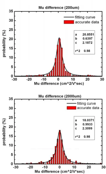
As for the distribution of the difference of Mu, the Lorentzian distribution is apply to the fitting, which is 1 2 a y= x - b + c ⎛ ⎞ ⎜ ⎟ ⎝ ⎠ where
a is the peak value of the distribution b is the center of the distribution
c is fitting parameter related to the width of the distribution
The Mu difference distributions of N-type and P-type TFT with different device distance are shown in Fig. 2-12 and Fig. 2-13. The values of R square of the above fittng curves are both higher than 0.85. It clearly shows the good fitness of our proposed mathemtical model and most of the fitting parameters slightly changing with distance, which supports the effects of macro variation are minor than those of micro variation we mentioned before.
Fig. 2-1 The layout of the crosstie TFTs
Fig. 2-4 The initial distribution of P-type TFT threshold voltage (Vth)
Fig. 2-6 A chart demonstrates device parameter distribution along distance corresponding to the concept of noise
Fig. 2-7 A chart demonstrates device parameter distribution along distance corresponding to the concept of signal and noise
Fig. 2-8 The average and standard deviation of TFT threshold voltage (Vth) difference
Fig. 2-13 The distribution of P-type TFT mobility (Mu) difference