鎳-磷-鑽石奈米複合材料之複合效應於材料特性差異上的研究
43
0
0
全文
(2) 鎳-磷-鑽石奈米複合材料之複合效應於材料特性差異上的研究 The Investigation of Property Distinction in Ni-P-Diamond Nanocomposite System. 研 究 生:蔣宜達. Student:I-Ta Chiang. 指導教授:鄭裕庭. Advisor:Yu-Ting Cheng. 國 立 交 通 大 學 電子工程學系電子研究所 碩 士 論 文. A Thesis Submitted to Department of Electronics Engineering & Institute of Electronics College of Electrical Engineering and Computer Science National Chiao-Tung University in Fulfillment of the Requirements for the Degree of Master in Electronics Engineering July 2004 Hsinchu, Taiwan, Republic of China. 中華民國九十五年一月.
(3) 鎳-磷-鑽石奈米複合材料之複合效應於材料特性差 異上的研究 學生:蔣宜達. 指導教授:鄭裕庭教授. 國立交通大學電子工程系暨電子研究所碩士班. 摘. 要. 先前我們已經發表過在鎳基材中摻入如二氧化矽、鑽石、碳管等奈米 微粒可以改變鎳金屬的機、電特性。這些特性的改善使得奈米複合材料在 微機電的應用上具有很大的發展性。為了更進一步的應用這些奈米複合材 料、有效控制材料特性來製作元件,我們必需對複合材料特性做更深入的 研究,了解在奈米微粒不同粒徑、外型及在基材中不同的分怖情形時所造 成的特性差異。到目前為止,只有少數的研究針對這些問題去做探討。在 本篇論文中將報告一個在鎳-磷-鑽石奈米複合材料中觀察到的有趣現象, 即在摻雜相同的二相材料進入不同微結構的鎳基材時將產生不同的材料特 性變化。奈米壓痕儀的量測結果指出,在奈米鑽石微粒體積百分比 4%含量 下且微結構為非晶型態的鎳-磷-鑽石複合材料薄膜其硬度值從純鎳-磷薄 膜的 6.7GPa提升到 7.5GPa,反觀微結構由非晶及奈米晶粒所組成的鎳-磷鑽石薄膜其硬度值隨著奈米鑽石微粒含量的增加能下降。同時,量測每公 升鍍液裡有 2 克的奈米鑽石微粒溶液中鍍出來的鎳-磷-鑽石複合材料薄膜 i.
(4) 電性可以發現,非晶結構的鎳-磷-鑽石複合材料比微結構為非晶及奈米晶 粒所組成的鎳-磷-鑽石複合材料有更好的導電性,其相對應的量測電阻率 -6. -6. 分別為 1.125*10 Ω-m及 1.561*10 Ω-m。另一方面,由鎳-磷-鑽石複合材 料所製成的電熱式微致動器,無論在何種微結構下其最大位移量均比由純 鎳-磷材料所製成的微致器來的大,此外,非晶型態的鎳基材電熱式微致動 器比微結構為非晶及奈米晶粒所組成的鎳基材微致動器有更佳的電源效 率。我們相信這些觀察到的現象將引起材料學者及元件工程師在複合材料 的理論研究及應用上的興趣。. ii.
(5) The Investigation of Property Distinction in Ni-P-Diamond Nanocomposite System Student : I-Ta Chiang. Advisor : Yu-Ting Cheng. Department of Electronics Engineering & Institute of Electronics National Chiao Tung University. Abstract Previously, we have reported that incorporating nanoparticles, such as SiO2, diamond, and carbon nanotube (CNT) into a nickel matrix can change the mechanical and electrical properties of pure nickel.. The property. modifications have shown a great potentiality of the nanocomposites for MEMS applications.. However, for the advancement of the applications, it is required. to further investigate on the material property modification resulted by nanocomposite effects, such as particle size, shape, and distribution effects on the matrix, from which the material properties can be well engineered for designated device fabrication. So far, few researches have been worked on the related issues.. In the thesis, an interesting phenomenon is observed and. reported in Ni-P-Diamond nanocomposite system, in which the microstructure difference of Ni matrix would result in distinct property modifications even though the same second phase material is added.. The nanoindentation. measurement shows that the Young’s modulus and harness of the amorphous iii.
(6) crystallization of the Ni-P films can increase from 6.7Gpa to 7.5Gpa while 4% volume fraction of nano-diamonds are incorporated. In contrast, the modulus and hardness of the Ni-P films with a mixed microstructure of nanocrystalline and amorphous phase decrease with the incorporation of the nano-diamonds. Meanwhile, from the electrical measurements of the 2g/L Ni-P-Diamond nanocomposite films, it is found that the resistivities of these two Ni-P-Diamond nanocomposites are 1.125*10-6Ω-m and 1.561*10-6Ω-m, respectively for an amorphous matrix and a matrix with the mixtures of nanocrystalline and amorphous phase, which indicating the Ni-P-Diamond nanocomposite with amorphous Ni matrix has better electrical conductivity than the other.. Since it. is found that the electrothermal microactuator made of both Ni-P-Diamond nanocomposites can exhibit a larger ultimate elongation than that made of pure Ni-P and the actuator made of the nanocomposite with fully amorphous Ni matrix can have a better power-efficient performance as compared, it is our belief that the observations would lead a great interest to material scientists and device engineers in the future development of nanocomposite synthesis and theory.. iv.
(7) 誌. 謝. 首先,我要感謝的家人,爸爸、媽媽、還有弟弟,謝謝你們在這段期 間對我精神上、生活上的支持,對於一個快 30 歲的人還沒辦法對家裡有所 貢獻,反而還需要你們的支助,我真的很感謝,家人永遠是最好的支持者, 我很慶興有你們當家人。爸、媽,現在我畢業了,我和阿興將盡力讓你們 過安祥舒適的日子,畢竟你們為這個家辛苦了一輩子,是該好好休息一下 換我和阿興接手了。 此外,我要感謝我的指導老師鄭裕庭教授,謝謝你在這段期間對我的 指導,謝謝!!另外,我還要感謝交大材料所蔡欣瑩小姐及陳曉雲學姐,謝 謝你們對一個完全不相干的人伸出援手,幫我做量測,非常感謝。 當然我還要跟我們實驗室的伙伴們說聲謝謝,學姐、光仁、志瑋、凱 哥、子元、健章、chando、小 b、思穎、昱文還有過很爽的助理小筑^^,謝 謝大家有共同的目標,能一起哈啦打屁、發洩心情,剩下來的看你們了, 加油吧,忍一忍、撐一下就過了,大家的目標都一樣,光仁他們是如此, 我們也是如此,你們也一樣,不過我能說的,也只是~~~加油。 最後我要謝謝另一個在背後支持我的人,我的女朋友怡青,謝謝你陪 我走過來,聽我訴苦,也很抱歉這段日子都沒帶你出去玩,歹勢啦^^|. 宣告:給我的猪朋狗友們,別再問我到底什麼時候要畢業了,別再說我變 遜了,我沒變遜,我畢業了,我的階段任務完成了,我回來了,雖然我知 道你們現在薪水都上 50k 了,但我會努力追上你們的,小心啦~~~~. v.
(8) 摘要. i. Abstract. iii. 誌謝. v. Contents. vi. Figure Captions. vii. Table Captions. ix. Contents Chapter 1 Introduction. 1. Chapter 2 Concept Design and Sample Preparation. 4. 2.1 Concept Design of the Electrothermal Microactuator. 4. 2.2 Sample Preparation. 5. 2.2.1 Electroless Ni-P-Diamond Plating Solution Preparation. 5. 2.2.2 Fabrication Process of the Electrothermal Microactuator. 6. Chapter 3 Results and Discussions. 9. 3.1 The SEM photograph. 9. 3.2 Phosphorus content and Crystallization analysis. 9. 3.3 The Element Analyzer (EA) Analysis. 15. 3.4 The Nano-Indentation tests. 16. 3.5 Electrical Property Analysis. 21. 3.6 Displacement Measurements of the electrothermal Microactuator. 23. Chapter 4 Summary and Future Work. 28. 4.1 Summary. 28. 4.2 Future Work. 29. References. 30 vi.
(9) Figure Captions Chapter 2 Fig. 2-1 The Concept Design of an Electro-Thermal Microactuator Fig. 2-2 The electroless plating equipments setup. 4 6. Fig. 2-3 The electrothermal microactuator process flow chart. 8. Chapter 3 Fig. 3-1 The SEM photo of Ni-P-Diamond deposition surface (a) case 1 11. (b) case 2 Fig. 3-2 The fabricated electrothermal microactuator. 12. Fig. 3-3 The EDS diagram (a) pure Ni-P film (b) case 1 of the Ni-P-Diamond film (c) case 2 of the Ni-P-Diamond film. 13. Fig. 3-4 The X-ray diffraction profile. (a) case 1 (b) case 2. 14. Fig. 3-5 The plot of diamond volume fractions versus plating bath 15. concentrations Fig. 3-6 The measured Young’s modulus of case 1. (a) pure Ni-P (b) 0.5g/L diamond (c) 1g/L diamond (d) 2g/L diamond. 18. Fig. 3-7 The measured hardness of case 1. (a) pure Ni-P (b) 0.5g/L diamond (c) 1g/L diamond (d) 2g/L diamond. 19. Fig. 3-8 The comparison of the curves with measured and ROM. (a) case 1 20. (b) case 2 Fig. 3-9 The resistivity versus diamond concentration curve of the Ni-P-Diamond nanocomposite films. vii. 23.
(10) Fig. 3-10 The diagram of power-displacement for Ni-P-Diamond electrothermal microactuator. (a) case 1 (b) case 2. 25. Fig. 3-11 The measured of power-displacement for electrothermal 26. microactuators. Fig. 3-12 The diagram of power-displacement for electroplating Ni-Diamond electrothermal microactuators. 26. Fig. 3-13 The plot of the measured CTE values. 27. viii.
(11) Table Captions Chapter 1 Table 1-1 The advantage and disadvantage of the polysilicon and metal materials in MEMS application.............................................................3 Table 1-2 Relationship between the crystallization and the phosphorus contents 3. of EN films. Chapter 3 Table 3-1 The measured weight fractions and volume fractions of two cases with different diamond concentrations………………………………..15 Table 3-2 The measured sheet resistance and resistivity of Ni-P-Diamond composite films……………………………………………………….22 Table 3-3 The measured CTE values…………………………………………..27. ix.
(12) Chapter 1 Introduction In the contemporary fabrication process of microelectromechanical system (MEMS) devices, the polysilicon and metal, such as Cu, Al, and Ni, are the main materials due to their excellent mechanical and electrical properties. But these materials are existence some deficiency. For example, the highly-doped polysilicon deposition should be processing under high temperature (>1000℃) environment, this processing temperature makes itself not suitable for CMOS integration. In addition, the metal materials have aging and fatigue issues. Table 1-1 shows the advantages and disadvantages of these materials. In order to practice a post-COMS MEMS integration, it is necessary to develop a low temperature process. Base on this, we have proposed a selective electroless nanocomposite deposition techniques [1,2,3] previously. We had successfully used Ni-base nanocomposites to make a MEMS device that the device can be made below 100℃ and also have good properties. Utilizing the structure material with second phase effects to enhance device performance. makes. nanocomposite. materials. fascinating. in. recent. nanotechnology development. Various metal/ceramic nanocomposites have been synthesized and proposed for potential applications such as tribological coating, gas sensing, and RF [4,5,6]. A metal incorporated with well distributed ceramic nanopowders like Al2O3, Si3N4, SiO2, diamond, and Fe(II, III) oxide can have homogeneous material property modification including the augment of hardness,. 1.
(13) Young’s modulus, coefficient of thermal expansion (CTE), or coercivity that is beyond its intrinsic characteristic limit. Since it has been found that the residual stress of nanocomposite film can also be customized with adequate incorporation of nanoparticles for the fabrication of microactuators, related investigations on property characterization become critical for further applications. Previously, we have many investigations on the Ni-based nanocomposite, but all of that are focused on second phase effects. However, many investigations have been reported that the phosphorus contents of the EN films can effect upon the crystallization and microstructural properties. [7,8,9] Based on phosphorus contents, the electroless nickel (EN) deposits can classified as low (1~5 wt% P), medium (5~9 wt% P) and high (>9 wt% P) phosphorus content. Table 1-2 shows that the crystallization on different phosphorus contents. Therefore, in this thesis, we will report an interesting phenomenon observed. in. Ni-P-diamond. nanocomposite. systems.. Totally. distinct. nanocomposite effects on the material property enhancement resulted by the difference of matrix microstructure are found even though the matrix and secondary phase materials are the same.. 2.
(14) Table 1-1 The advantage and disadvantage of the polysilicon and metal materials in MEMS application. Polysilicon Advantage. Metal. 1.Good mechanical properties 2.CTE close to Si substrate. 1.Low fabrication temperature 2.Good electrical conductivity. 1.Aging and fatigue problem 1.High fabrication temperature 2.CTE mismatch to Si substrate Disadvantage 2.High resistivity 3.Residual stress problem. Table 1-2 Relationship between the crystallization and the phosphorus contents of EN films.[8,10-12] Phosphorus contents (wt%) Low. Medium. High. Crystallization. 1~5. 1.Crystalline 2.Consist of microcrystalline nickel. 5~9. 1.Fully amorphous 2.Mixtures of microcrystalline nickel and amorphous. 9 and above. 1.Fully amorphous 2.Mixtures of microcrystalline nickel and amorphous 3.Consist of 2 and various other phases such as Ni5P4, Ni12P5, Ni5P2. 3.
(15) Chapter 2 Concept Design and Sample Preparation 2.1 Concept Design of the Electrothermal Microactuator The electrothermal microactuator is based on the long-short beam design [13] as shown in Fig. 2-1. The device structure is consists of two anchor pads and a pair of adjacent cantilever beams with different lengths that connect in one end. By resistively heating these two beams, unequal thermal expansions make the joint of the beams toward to the shorter one and provide a lateral actuation. In our design, the length of the long beam is 800μm and the short beam is 400μm, both beams wide and the gap between these two beams are 10μm. With the fixed plating parameter, the thickness of the actuator is about 7μm. V. Fig. 2-1 The Concept Design of an Electro-Thermal Microactuator.[13]. 4.
(16) 2.2 Sample Preparation 2.2.1 Electroless Ni-P-Diamond Plating Solution Preparation To make a good Ni-P electroless thinfilm or devices, the plating solution is an important point to attention, because some commercial plating solution would cause deposited surface rough. As the Ni-P-Diamond electroless plating, well dispersed diamond powders can ensure the powders uniformly engulfed into nickel matrix during the processing. In our study, prepare of 1 liter Ni-P-Diamond plating bath, a commercial Ni-P plating bath [14] composed of 150mL Sheng-Hung chemical nickel plating SCNP A solution and 150mL SCNP B solution is first mixed with prewetted diamond powder (average size<0.5μm, density: 3.51g/cm3) solution. Then utilize D.I. water and NH4OH to modify the pH value to 4.6 and make the total solution volume 1 liter. During plating process, good stir of the plating solution can keep the diamond powders dispersive well for uniform deposition of Ni-P-Diamond nanocomposite. The plating solution with different diamond concentrations are premeditated to characterize fabrication process and material property, which are 0, 0.5, 1, and 2 gram of the diamond powders per liter of plating solution, respectively. Fig. 2-2 illustrate the total setup of the electroless plating equipment.. 5.
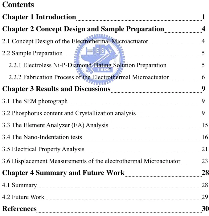
(17) Fig. 2-2 The electroless plating equipments setup.[15]. 2.2.2 Fabrication Process of the Electrothermal Microactuator The electrothermal microactuator structure is shown in Fig. 2-1. The fabrication process flow described in below, and the Fig. 2-3 is the relative process flow chart. Step1: After standard RCA clean, a 2μm HDP-CVD SiO2 is deposited on the 4 inch silicon wafer as the electrical insulation and sacrificial layer. Step2: Sputter a Ti/Cu (100Å/500Å) seed layer on the top of the SiO2. Step3: Coating a 10μm thick AZP-4620 photoresist (PR) to mold the device structure.. 6.
(18) Step4: Put the wafer into the Pd seeding solution for 30seconds to active the copper surface. After being seeded, the wafer put into the Ni-P or the Ni-P-Diamond plating bath for 7μm thick nanocomposite film deposition. During the plating process, the temperature of plating bath is kept at 78℃ and also kept the plating solution circulation well. Step5: Released the structure. First, utilize the acetone and NH4OH+H2O2 to removal the mold of PR AZP-4620 and copper seed layer. Then, by dipping the wafer into HF to etch the Ti seed layer and the SiO2 sacrificial layer under the beams. In order to prevent the suspending structure sticktion, after the structure released, put the wafer into the IPA and then baked at 90℃. Finally, the device is done.. 7.
(19) Step 1. Step 2. Step 3. Step 4. Step 5. Si Wafer. SiO2. Ti/Cu seed layer. EN deposited. Fig. 2-3 The electrothermal microactuator process flow chart.. 8.
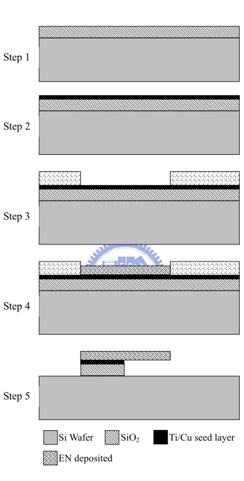
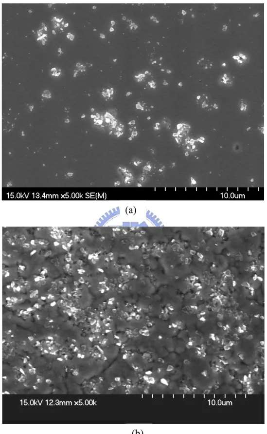
(20) Chapter 3 Results and Discussions In this chapter, we will report the properties which we observe in Ni-P-Diamond nanocomposite that has different matrix microstructure. In order to easy for the report and discussion later, here we define: Case 1 represents the fully amorphous phase crystallization. Case 2 represents the mixtures of microcrystalline nickel and amorphous phase crystallization.*. * The data about case 2 are extracted from Shen’s thesis. [15] 3.1 The SEM photograph The Scanning Electro Microscope (SEM) photograph of the Ni-P-Diamond nanocomposite deposition surface and electrothermal microactuator are shown in the Fig. 3-1 and Fig. 3-2. Based on the Fig. 3-1, we can confirm that the diamond powder is embedded in the nickel matrix. Furthermore, Fig. 3-1(b) shows that the case 2 of Ni-P-Diamond nanocomposite deposition has some cracks and voids; it is not our desired because the defect would result in bad properties of nanocomposite.. 3.2 Phosphorus content and Crystallization analysis Many investigations have been reported that the phosphorus contents of the electroless nickel films can effect upon the crystallization and microstructural properties. Also we believe, the phosphorus content will effect on the property. 9.
(21) of the electroless nickel based nanocomposite. Therefore, ensure the phosphorus content in the Ni-P-Diamond is very important in this study. The Energy Dispersive Spectroscopy (EDS) is utilized to analyze phosphorus content of the Ni-P-Diamond nanocomposite deposition. By EDS analyze, the phosphorus content is 7.32wt% and 7.11wt% respectively corresponding to the case 1 and case 2. Both of two cases are taken into medium phosphorus content class. Fig. 3-3 shows the EDS diagram. Through the EDS diagram, the carbon peaks indicate again that the diamond powder is real existence in the Ni-P-Diamond nanocomposite deposition. The X-ray diffractometer, PHILIPS X’Pert Pro (MRD) is utilized to analyze the crystallization of the EN-based depositions. The XRD profiles of the case 1 and 2 are shown in Fig. 3-4. In the Fig. 3-4(b), the Ni(111) peak appear at the angle about 44.8°, and the broad width peak of the amorphous Ni phase is also revealed and overlapped with the Ni(111) microcrystalline peak. Compare the X-ray profiles between the case 1 and case 2, the data show that they are different matrix microstructure. However, the amorphous phase will transform into crystalline after the high temperature annealing. But it is no any annealing process in our study, because the working temperature is not suitable for post –COMS MEMS integration. By the EDS and X-ray data, we can see that it is different crystallization in the medium phosphorus content. It is conformed to other investigated report.. 10.
(22) (a). (b) Fig. 3-1 The SEM photo of Ni-P-Diamond deposition surface (a) case 1 (b) case 2. 11.
(23) (a). (b) Fig. 3-2 (a) (b) The fabricated electrothermal microactuator.. 12.
(24) (a). (b). (c). Fig. 3-3 The EDS diagram. (a) pure Ni-P film (b) case 1of the Ni-P-Diamond film (c) case 2 of Ni-P-Diamond film 13.
(25) 2000 1800. In te n s ity [A rb .U n its ]. 1600 1400 1200 1000 800 600. amorphous. 400 200 0 15. 20. 25. 30. 35. 40. 45. 50. 55. 2θ[deg.]. (a). (b) Fig. 3-4 The X-ray diffraction profile. (a) case 1 (b) case 2. 14.
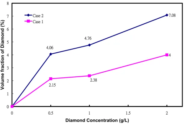
(26) 3.3 The Element Analyzer (EA) Analysis The volume fractions of diamond powders within Ni-P-Diamond deposit should be conformed to make a further comparison and discussion for various measurements. With EA analysis, the weight fractions of the diamond powders in the Ni matrix can be corroborated. Then the volume fractions of diamond powders in the deposit can be obtained by the variables transformation from the density of nickel (8.908g/cm3) and the density of diamond powder (3.51g/cm3). The weight fractions and volume fractions of the diamond powders in the Ni-P-Diamond films are shown in Table 3-1. Fig. 3-5 shows the diagrams of volume fractions of diamond powders versus the concentrations of the plating bath. We can see that with the same process conditions, more diamond powders which is two times of that in case 1 can be contained in case 2. By this data and SEM graphics shown in Fig. 3-1, we can observe that too many diamond powders content would cause the deposit results crack, what’s influence resulted from this defect will observe by Nano-Indentation test and discussion after. Table 3-1 The measured weight fractions and volume fractions of two cases with different diamond concentrations. Case 1 -Diamond concentration (g/L) 0 0.5 1 2 Weight fraction Volume fraction. *. Case 2 -Diamond concentration (g/L) 0 0.5 1 2. 0%. 0.84% 0.93% 1.55%. 0%. *. 1.58% 1.84% 2.72%. 0%. 2.15% 2.38%. 0%. 4.06% 4.76% 7.08%. 4%. *The actuality measure value is 0.05%. 15.
(27) 8. Volume fraction of Diamond (%). 7.08. Case 2 Case 1. 7 6. 4.76. 5 4.06 4. 4. 3 2.38. 2 2.15 1 0 0. 0.5. 1. 1.5. 2. Diamond Concentration (g/L). Fig. 3-5 The plot of diamond volume fractions versus plating bath concentrations.. 3.4 The Nano-Indentation tests For the characterization of nanocomposite effects, the Ni-P-Diamonds films are deposited in EN-based solutions with different concentrations of diamond powders, which are 0, 0.5, 1, 2g/L, respectively. For case 1, Fig. 3-6 and Fig. 3-7 show the Young’s modulus and hardness values of nano-indentation test results. Here the Rule of Mixtures (ROM) [16,17] can be applied to estimate the physical properties of the composite material. According to the rule, the effective Young’s modulus of the Ni-P-Diamond has the upper-bound and low-bound values that are estimated as:. 16.
(28) E. E. eff. eff. = E cf c + E m f m. for the upper-bound. E mEc E m f c + E cf m. for the lower-bound. =. Where Ec, fc, Em and fm are the Young’s modulus and volume fraction of the diamond powder and nickel matrix, respectively. The theoretical value of Ec is 1100GPa for diamond and the volume fraction is shown in Table 3-1. The measurement and estimate values of case 1 and case 2 are show in Fig. 3-8. The data shows that the measured Young’s modulus is more close to the Low-bound in case 1. It is due to the relative modulus ratio (Ec/Em) is high and low volume fraction of the diamond powders, so the effective modulus is approach that of the Ni matrix. Similar study has been reported in Kim’s research. [18] Also we can see that compared to the pure Ni-P film, hardness value increases in case 1 but decreases in case 2 with increase the diamond powders content. This difference may result from cracks and voids. However, compared with the case 1 and case 2, the case 1 has better mechanical strength then suitable for device applications.. 17.
(29) (a). (b). (c). (d). Fig. 3-6 The measured Young’s modulus of case 1. (a) pure Ni-P (b) 0.5g/L diamond (c) 1g/L diamond (d) 2g/L diamond. 18.
(30) (a). (b). (c). (d). Fig 3-7 The measured hardness of case 1. (a) pure Ni-P (b) 0.5g/L diamond (c) 1g/L diamond (d) 2g/L diamond. 19.
(31) 200. 16 191.84. 174.34. 176.51. 156.9. 157.22. 14. 154. 157.9. 154.4. 155.5. 12 10. 120 7.47. 7.58. 7.49. 6.7 80. 8 6. ROM modulus (U.B.) ROM modulus (L.B.) measured modulus measured hardness. 40. Hardness (Gpa). Young's Modulus (GPa). 160. 159.49. 4 2. 0. 0. 0. 0.5. 1. 1.5. 2. Diamond Concentration (g/L). (a) 16. 250 231.32 209.57. 203.07. 14. 171.07 165.1. 150. 12. 172.14. 175.81. 169.4. 10 153.6 8. 6.7 100. 110.5. 6.1. 6. 5.1. 4. ROM modulus (U.B) ROM modulus (L.B.) measured modulus measured hardness. 50. 2.3. 0. 2 0. 0. 0.5. 1. 1.5. 2. Diamond Concentration (g/L). (b) Fig. 3-8 The comparison of the curves with measured and ROM. (a) case 1 (b) case 2. 20. Hardness (GPa). Young's Modulus (GPa). 200.
(32) 3.5 Electrical Property Analysis The 4-point probe is utilized to measure the sheet resistance of the Ni-P-Diamond films. The intrinsic bulk resistivities of EN-based of nanocomposite film are obtained by multiplying the sheet resistance by film thickness. Table 3-2 shows the measurement results. The data shows the resistivity increases with the incorporated diamond powders concentration, because the diamond powder is an insulator that contributes no electrical conductivity to the Ni matrix. Based on the model of two-phase random network, the Maxwell-Wanger equation [19] described in Eq. 1 is utilized for the characterization of the electrical conductivity of the composites.. 1+ 2V (1− km/k )/(1+ 2km/k ) f d d kc = km 1− V (1− km/k )/(1+ 2km/k ) f d d. (1). Where Kc is the conductivity of the Ni-based composite film, Km is that of the Ni matrix, Kd that of the second phase composite, Vf the volume fraction of the second phase. Here, Eq. 1 can be approximated in Eq. 2 with Km » Kd for Ni-P-Diamond films, because the diamond is an insulator.. k c = k m (1 − V )/(1 + V /2) f f. (2). Substituting the know parameters Km and Vf into the Eq. 2, the conductivity of the Ni-P-diamond films can be obtained and transform it into the resistivity that. 21.
(33) shown in the Fig.3-9. We can see that the large discrepancy between the measurement results and theoretical predictions. In case 2, this discrepancy might result from the increase of cracks and voids, but this conjecture is not existence in case 1, what reason to cause this phenomenon should be further discussion.. Table 3-2 The measured sheet resistance and resistivity of Ni-P-Diamond composite films. Case 1. Rs(mΩ/□). avg. Film. Case 2. Pure Ni. 0.5g/L D. 1.0g/L D. 2.0g/L D. Pure Ni. 0.5g/L D. 1.0g/L D. 2.0g/L D. 155.2. 143.6. 150. 172.5. 310. 83.1. 94.4. 121.6. 146.3. 143.6. 147.5. 171.3. 315. 85.2. 95.8. 119.5. 146.2. 142.9. 147.3. 170.9. 327. 84. 106.2. 120.4. 146. 140.8. 146.9. 170.7. 351. 83.3. 92.3. 113.5. 145.6. 139.5. 146.7. 167.8. 349. 85.8. 94.9. 117.4. 145.4. 139. 146.2. 167.2. 331. 80. 93.7. 114.2. 145. 138.6. 145.8. 166.9. 326. 81.6. 86.4. 110.9. 145. 137.6. 143.7. 165.2. 319. 84.1. 89. 104.4. 143.5. 137.1. 143.4. 164.5. 346. 81.1. 86.3. 111.6. 146.17. 139.68 145.93. 167.96. 330.4. 83.1. 93.2. 114.8. 5.95. 7. 7.3. 6.7. 3.8. 16.2. 16.3. 13.6. 869.71. 977.76. 1065.3. 1125.3. 1255.7. 1346.8. 1519.5. 1561.3. thickness(μm) Resistivity -9. ρ(10 Ω-m). 22.
(34) 1800 1519.5. 1600 1346.8. 1400. Resistivity (10^-9Ω-m). 1561.3. 1200. 1255.7. 1335.41. 1399.22 1349.84 1065.29. 1125.33. 977.76. 1000. 924.07 800. 869.71. 898.38. 901.52. 600. 4-pt prob (case 2) Maxwell approx. (case 2) 4-pt prob (case 1) Maxwell approx. (case 1). 400 200 0 0. 0.5. 1. 1.5. 2. Diamond Concentration (g/L). Fig. 3-9 The resistivity versus diamond concentration curve of the Ni-P-Diamond nanocomposite films.. 3-6. Displacement. Measurements. of. the. electrothermal. Microactuator The measurement results of electrothermal microactuator plated in different concentrations of Ni-P-Diamond plating solutions are shown in Fig. 3-10. In the measurement, different voltages applied on the two anchors to electrically heat the two beams (see in Fig. 2-1). The tip of the beam will curve to the direction of the short beam due to the different elongations result from different beam lengths. The data reveals that the mechanical strength of the actuator made of Ni-P-Diamond nanocomposite has been improve in comparison with that made of the pure Ni-P. Fig. 3-11 shows the measurement results of case 1 and case 2. 23.
(35) plated in pure Ni-P and 2g/L Ni-P-Diamond plating bath. We can observe that the maximum displacement of actuator made of 2g/L Ni-P-Diamond can reach 10μm in both cases, which are 1.5 times larger in case 1 and 4 times larger in case 2 than that of the pure one, respectively. Here are different results in power efficiency between with the case 1 and case 2, at the same displacement, the Ni-P-Diamond nanocomposite film has better power efficiency than that of the pure one in case 2, but it is opposite in the case 1. Previously, we have reported the similar investigate in electroplating Ni-Diamond nanocomposite system [20], the measurement result is similar to the case 2 that the Ni-Diamond nanocomposite film has better power efficiency, Fig. 3-12 shows the plot of the measurement results. This difference may result from the different coefficient of thermal expansion (CTE). The measured of CTE values shown in Table 3-3 and is plotted in Fig. 3-13. By the measured displacement of the microactuator and CTE values, we can observe that the power efficiency is proportion to the CTE value. However, compare the case 1 and case 2, the lower trigger power is needed in case 1 than that in case 2 whatever pure Ni-P film or Ni-P-Diamond films. Here is a question should be study continued that what is the role of the diamond powders play in here. It should be further investigate to understand, why Ni-P-Diamond nanocomposite electrothermal microactuator has longer maximum displacement than that of the pure one.. 24.
(36) 12. Pure Ni-P 0.5g/L Diamond 1g/L Diamond 2g/L Diamond. Displacement (μm). 10. 8. 6. 4. 2. 0 0. 0.05. 0.1. 0.15. 0.2. 0.25. Power (W). (a) 12 0.5g/L diamond 1.0g/L diamond 10. 2.0g/L diamond. Displacement (μm). pure Ni 8. 6. 4. 2. 0 0. 0.05. 0.1. 0.15. 0.2. 0.25. 0.3. 0.35. Power (w). (b) Fig. 3-10 The diagram of power-displacement for Ni-P-Diamond electrothermal microactuator. (a) Case 1 (b) Case 2. 25.
(37) 12. Pure Ni(case 1) 2g/L Diamonds(case 1) Pure Ni(case 2) 2g/L Diamonds(case 2). Displacement (μm). 10. 8. 6. 4. 2. 0 0. 0.05. 0.1. 0.15. 0.2. 0.25. 0.3. Power (W). Fig. 3-11 The measured of power-displacement for electrothermal microactuators. Fig. 3-12 The diagram of power-displacement for electroplating Ni-Diamond electro-thermal microactuators. 26.
(38) Table 3-3 The measured CTE values.. Plating technology. Diamond concentration. CTE (ppm/℃). Pure Ni-P. 13.4*10. Electroless. 0.5g/L Diamond. 13.19*10. (Case 1). 1g/L Diamond. 13*10. 2g/L Diamond. 10.81*10. Pure Ni. 27*10. 0.5g/L Diamond. 32*10. 1g/L Diamond. 46*10. 2g/L Diamond. 54*10. -6. -6. -6. -6. -6. -6. Electroplating. -6. -6. 60 Electroless (case 1) Electroplating. CTE (10-6/℃). 50. 54 46. 40 32 27. 30. 20 13.4. 13.19. 13 10.81. 10. 0 0. 0.5. 1. 1.5. Diamond concentration (g/L). Fig. 3-13 The plot of the measured CTE values.. 27. 2.
(39) Chapter 4 Summary and Future Work 4.1 Summary The properties of different crystallization of Ni-P-Diamond nanocomposites have been reported and compared. According to the mechanical and electrical property analyses and the device characterizations, we found that different crystallization incorporated with the same diamond powders would result in a totally distinct property modification in the Ni-P-Diamond nanocomposite system.. By nanoindentation analyze, the amorphous crystallization of Ni-P. films incorporated with the nano-diamond powders can improve the Young’s modulus and hardness then has better mechanical strength. In contract, the modulus and hardness of the Ni-P films with a mixed microstructure of nanocrystallize and amorphous phase decrease with the incorporation of the nano-diamonds. Furthermore, the measured data of resistivity of the Ni-P-Diamond. nanocomposite. films. reveal. that. the. Ni-P-Diamond. nanocomposite with amorphous Ni matrix has better electrical conductivity than the other. Meanwhile, from the displacement measurement of the electrothermal microactuator made of the Ni-P-Diamond composite, it is found that the maximum displacement of the actuator can be improve in both crystallization, and also we can see that the actuator made of the nanocomposite with fully amorphous Ni matrix have better power-efficient performance, in other word, the lower trigger power is needed in the fully amorphous Ni matrix of the pure. 28.
(40) Ni-P film and Ni-P-Diamond films. Finally, the properties of the Ni-P-Diamond nanocomposite with the different microstructure of Ni matrix have been reported. We believe that consider the second phase effect and the matrix microstructure simultaneously, it would be a great helpful to develop a high performance device for application.. 4.2 Future Work So far, we still don’t understand what reason it has different crystallization under the same plating solution and fabrication process, this issue is also an argument in other investigator. In order to make a crystallization of EN-based nanocomposite we want, this issue should be clear. Furthermore, in order to further demonstrate the Ni-P-Diamond nanocomposite properties, the other devices such as MEMS resonators and switches should be fabricated and measurement. An excellent performance on the MEMS devices could be expected in the future work.. 29.
(41) References 1. K.S. Teh, Y.T. Cheng, and C. Sambucetti,” Selective Plating of Nickel Ceramic Composite Films for MEMS Applications” IEEE Micro Electro Mechanical Systems Conference, Las Vegas, NV, 2002, pp. 384. 2. G..R. Shen, L.N. Tsai, Y.T. Cheng, W. Hsu, and T.K. Lin, “Ni-P-CNTs Nanocomposite Film for MEMS Applications”, IEEE Conference on Nanotechnology, Munchen, Germany, 2004, pp.192. 3. Tzu-Yuan Chao, Guang-Ren Shen, and Y.T. Cheng, “Comparative Study of Ni-P-Diamond and Ni-P-CNT Nanocomposite Films” accepted to Journal of The Electrochemical Society, 153 (1). 4. W.X. Chen, J.P. Tu, L.Y. Wang, H.Y. Gan, Z.D. Xu, and X.B. Zhang, “Tribological Application of Carbon Nanotubes in a Metal-based Composite Coating and Composites” Carbon, 41(2003), pp.215 5. Céline Nayral, Eric Viala, Pierre Fau, François Senocq, Jean-Claude Jumas, André Maisonnat, and Bruno Chaudret, “Synthesis of Tin and Tin Oxide Nanoparticles of Low Size Dispersity for Application in Gas Sensing” Chem. Eur. J., 6(2000), pp.4082. 6. Hai Dong, Fuhan Liu, C.P. Wong, “Magnetic Nanocomposite for High Q Embedded Inductor”, 9th Int’l Symposium on Advanced Packaging Materials, 2004, pp.171-174. 7. Luisa M. Abrantes, Alda Fundo and Gang Jin, “Influence of Phosphorus Content on the Structure of Nickel Electroless Deposits” J. Mater. Chem., 11(2001), pp.200-203. 8. P. Sampath Kumar and P. Kesavan Nair, “Studies on Crystallization of Electroless Ni-P Deposits”, Journal of Materials Processing Technology, 56(1996), pp.511-520. 9. K.G. Keong, W. Sha, S. Malinov, “Crystallisation Kinetics and Phase Transformation Behaviour of Electroless Nickel-Phosphorus Deposits with High Phosphorus Content”, J. Alloys Compd., 334(2002), pp.192-199. 10. K.G. Keong, W. Sha, S. Malinov, “Crystallization and Phase Transformation Behaviour of Electroless Nickel-Phosphorus Deposits with Low and 30.
(42) Medium Phosphorus Contents Under Continuous Heating“, Journal of Materials Science, 37(2002), pp.4445-4450.. 11. N.M. Martyak, K. Drake, “Peak-profile Analysis of Electroless Nickel Coatings“, J. Alloy. Compd., 312(2000), pp.30-40. 12. N.M. Martyak, “Characterization of Thin Electroless Nickel Coatings”, Chem. Mater., 6(1994), pp.1667.. 13. C.S. Pan, Wen Syan Hsu, “An Electro-Thermally and Laterally Driven Polysilicon Microactuator”, J. Micromech. And Microeng., 7(1997), pp.7-13 14. Sheng Hung Chemical Engineering Co., Ltd., http://www.schccl.com.tw 15. Guang-Ren. Shen,. “Properties. Enhancements. of. Ni-P-CNTs. and. Ni-P-Diamond Nanocomposites Films and the Applications on MEMS Device”, Master Thesis, National Chiao-Tung University, 2004 16. W. D. Callister, Jr., “Materials Science and Engineering, 3rd Ed.”, Chapter 17, John Wiley and Sons Inc., 1994, pp. 516-521 17. George. E.. Dieter,. “Mechanical. Metallurgy,. 3rd. Ed.”,Chapter. 6,. McGraw-Hill Book Company, New York, 1978, pp. 184-240 18. Hyoung Seop kim, “On the Rule of Mixtures for the Hardness of Particle Reinforced Composites”, Materials Science and Engineering A, 289(2000), pp.30-33 19. Dae Gon Han, and Gyeong Man Choi, “Computer Simulation of the Electrical Conductivity of Composites: the Effect of Geometrical Arrangement”, Solid State Ionics, 106(1998), pp.71-87 20. Li-Nuan Tsai, Guang-Ren Shen, Y.T. Cheng, and Wensyang Hsu, “Power and Reliability Improvement of an Electro-Thermal Microactuator Using Ni-Diamond Nanocomposite”, IEEE ECTC, Las Vegas, 2004, pp.472-476. 31.
(43) Vita 姓. 名:蔣宜達 (I-Ta Chiang). 出生日期:中華民國六十七年十月四日 出 生 地:台灣省台北縣 E - mail:[email protected] 學. 歷: 國立淡水商工電子科. (1993.9~1996.6). (National Tam-Shui Vocational High School) 私立景文技術學院電子科. (1996.9~1998.6). (Jin Wen Institute of Technology) 國立交通大學電子工程所碩士班. (2003.9~2006.1). (Department of electronics Engineering & Institute of Electronics, Nation Chiao Tung University). 32.
(44)
數據
![Table 1-2 Relationship between the crystallization and the phosphorus contents of EN films.[8,10-12]](https://thumb-ap.123doks.com/thumbv2/9libinfo/8748499.205392/14.892.121.792.210.497/table-relationship-crystallization-phosphorus-contents-en-films.webp)
![Fig. 2-1 The Concept Design of an Electro-Thermal Microactuator.[13]](https://thumb-ap.123doks.com/thumbv2/9libinfo/8748499.205392/15.892.108.802.528.995/fig-concept-design-electro-thermal-microactuator.webp)
![Fig. 2-2 The electroless plating equipments setup.[15]](https://thumb-ap.123doks.com/thumbv2/9libinfo/8748499.205392/17.892.148.789.170.499/fig-the-electroless-plating-equipments-setup.webp)
+7

![Fig. 3-4 The X-ray diffraction profile. (a) case 1 (b) case 2 02004006008001000120014001600180020001520253035404550552θ[deg.]Intensity[Arb.Units]amorphous(a)(b)](https://thumb-ap.123doks.com/thumbv2/9libinfo/8748499.205392/25.892.173.727.138.1005/fig-diffraction-profile-case-case-intensity-units-amorphous.webp)
Outline
相關文件
volume suppressed mass: (TeV) 2 /M P ∼ 10 −4 eV → mm range can be experimentally tested for any number of extra dimensions - Light U(1) gauge bosons: no derivative couplings. =>
For pedagogical purposes, let us start consideration from a simple one-dimensional (1D) system, where electrons are confined to a chain parallel to the x axis. As it is well known
The observed small neutrino masses strongly suggest the presence of super heavy Majorana neutrinos N. Out-of-thermal equilibrium processes may be easily realized around the
incapable to extract any quantities from QCD, nor to tackle the most interesting physics, namely, the spontaneously chiral symmetry breaking and the color confinement..
(1) Determine a hypersurface on which matching condition is given.. (2) Determine a
• Formation of massive primordial stars as origin of objects in the early universe. • Supernova explosions might be visible to the most
The difference resulted from the co- existence of two kinds of words in Buddhist scriptures a foreign words in which di- syllabic words are dominant, and most of them are the
(Another example of close harmony is the four-bar unaccompanied vocal introduction to “Paperback Writer”, a somewhat later Beatles song.) Overall, Lennon’s and McCartney’s
