國
立
交
通
大
學
電機資訊學院 電子與光電學程
碩
士
論
文
電 子 穿 越 肖 基 障 之 一 致 化 模 擬
A Unified Simulation of ElectronTransmission through the
Schottky Barrier
研 究 生:賴韋仲
指導教授:郭雙發 教授
電子穿越肖基障之一致化模擬
A Unified Simulation of ElectronTransmission through the
Schottky Barrier
學 生 : 賴韋仲 Student : Sierra Lai
指導教授 : 郭雙發 Advisor : Prof. Shuang-Fa Guo
國立交通大學
電機資訊在職專班 電子光電組
碩士論文
A Thesis of Master Degree
Institute of degree program of Electrical Engineering and Computer Science
Electronics and Optical Group
National Chiao-Tung University
June, 2005
Hsin-Chu, Taiwan, R.O.C 中華民國九十四年六月
電子穿越肖基障之一致化模擬
學 生 : 賴韋仲
指導教授
:郭雙發
教授國立交通大學電機資訊學院 電子與光電學程﹙研究所﹚碩士班
摘要
在此論文中我們已經發展一個數值模擬程式來探討電子穿越金屬版導體
接面的現象。能障的分布在半導體的表面被適當地分成幾個小區塊,能障位
能可近似一連串的線性區塊或階梯狀區塊。藉由 airy function 來解薛晶格
方程式可以產生一個轉移矩陣來表示每一小區塊裡的電子傳輸現象。電子穿
越整個接面能障的穿越係數可以每一小區塊的轉移矩陣相乘而得,並與傳統
的 WKB 近似法所求的穿越係數做比較。
不論電子能量大於或小於接面能障,電子傳輸係數都可以被計算出來,
所以我們首次提出電子穿越半導體表面及金屬半導體介面電子熱傳輸之一
致化模擬。傳輸係數是金屬至半導體電子移轉機率的方程式,而越過肖基障
的熱傳導電流可由經由對傳輸係數的積分而得。而電子穿越肖基障的電流則
可以轉成電子電動的合併及產生過程,此一過程與半導體的費米能階與未能
分佈有關。這電子穿越過程與半導體中電流的傳輸能自發性前後一致地連結
起來。
在不同傳輸模型及不同參雜濃度下的傳輸係數與電子能量的相關性及熱
A Unified Simulation of ElectronTransmission through the
Schottky Barrier
Student: Wei-Tsung Lai Advisor : Prof. Shuang-Fa Guo
Degree Program of Electrical Engineering Computer Science
National Chiao Tung University
Abstract
A numerical simulation program has been developed in this work to investigate the transmission of electrons through the metal-semiconductor contacts . The semiconductor surface is discretized properly into a number of small intervals and the potential barrier is approximated as a series of piece-wise linear or step functions. The transfer matrix for electron transmission through or cross each interval of simple potential distribution can be obtained by solving the Schrödinger equation using Airy or exponential function. The transmission coefficient of electrons through or across the whole contact barrier is then derived from the cascaded transfer matrices. As a com parison, the conventional WKB approximation method has also been illustrated.
Since the transmission coefficient can be calculated numerically for electron with energy below or above the contact barrier, we propose, for the first time, a unified simulation for electron tunneling through the semiconductor surface and thermionic -emission at the metal-s emiconductor interface. The thermionic-emission current across the Schottky barrier is integrated from the transmission coefficient, which is a function of electron energy together with the transition probability of electron between metal and semiconductor. However, the tunneling current through the Schottky barrier is converted into a local generation or recombination process with
local rate depending on the lo cal Fermi-level and the potential distribution. The tunneling processes are self-consistently treated with all current transport in the semiconductor.
The transmission coefficient is a function of electron energy as well as the tunneling and thermionic -emission currents as a function of applied voltage for different transmission models and various doping concentrations has been discussed in this paper.
誌
謝
During my study of this thesis, I would like to thanks Professor Guo very much. He spent a lot of time and had more pensions on me to do couching and guiding. I can not finish my thesis without him. I do appreciate all of his efforts. Besid es, my families, friends and colleagues also encourage and stick on me during the hard time of my work and study. The contribution of this work should belong to all related persons.
中文提要
………
i
英文提要
………
ii
誌謝
……… iv
目錄
………
v
圖目錄
……… vi
符號說明
……… viii
一、
Introduction
………
1
二、
Theory and Model
..………
5
2.1
Analytic Solutions of Schrödinger Equation………
5
2.2
Transfer Matrix for a Single Barrier………
8
2.3
Transmission Coefficient……… 11
2.4
WKB approximation for Arbitrary Potential………
13
2.5
Currents through the Schottky Barrier……… 17
三、
Numerical Techniques
……… 19
3.1
Space Discretization……… 19
3.2
Transfer Matrix Formulation……… 21
3.3
Discretization of Device Equations … … … ..21
3.4
Boundary Conditions… … … ...27
3.5
Generation Rate… … … ...29
四、
Results and Discussion
……… 31
4.1
Transmission Coefficients……… 31
4.2
Transition Probability……….. 34
4.3
Generation Rate… … … ...36
4.4
Current Density… … … .38
五、
Conclusions
………
43
參考文獻
……… 44
附錄一
……… 46
附錄二
……… 48
圖目錄
Fig. 2.1 Electron Transmission through Various Potentials Fig. 2.2 Trapezoidal Potential Barrier
Fig. 2.4.1 Potential distribution of Schottky barrier\
Fig. 2.5.1 Transmission coefficient vs. electron energy by (a) Airy function (b) WKB
approximation of trapezoidal barrier
Fig. 2.5.2 Transmission coefficient vs. barrier width by (a) Airy function (b) WKB
approximation of trapezoidal barrier
Fig. 3.1.1 Piecewise linear approximation for Schottky Barrier. Fig. 3.1.2 Step approximation for Schottky Barrier
Fig 3.4 Energy Band diagram of metal-n type semiconductor junction under
forward-biased condition
Fig 3.5. Generation rate due to tunneling in the bulk of the barrier and thermoinic
emission at the metal-semiconductor interface.
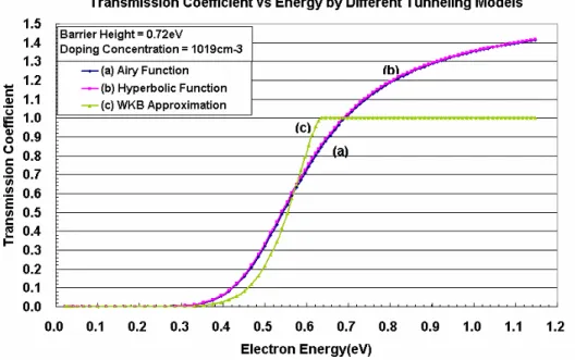
Fig 4.1.1 Transmission coefficient vs electron energy calculated by (a) Airy function
s olution (b) exponential solution (c) WKB approximation under conditions of barrier height 0.72eV and doping concentration 1019cm-3 at zero apply voltage
Fig 4.1.2 Transmission coefficient vs electron energy calculated by Airy function
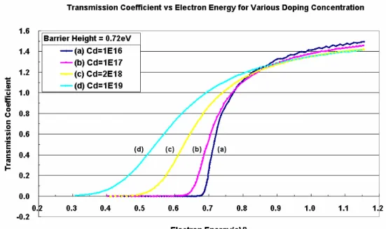
s olution for doping concentration of a) 1016 cm-3, b) 1017 cm-3, c) 2*1018 cm-3, d) 1019 cm-3 under conditions of barrier height=0.72eV at zero apply voltage
Fig 4.1.3 Space distribution of transmission coefficient calculated by (a) Airy function
and (b) WKB approximation, under conditions of barrier height 0.72eV , doping c oncentration= 1020cm-3 and zero apply voltage
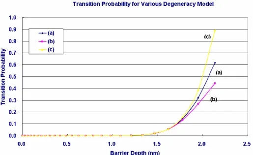
Fig 4.2.1 Space distribution of transition probability by using a) Degenerated model b)
Non-degenerated model ,and c) Maxwell-Bolzman model under conditions of doping concentration 1019 c m-3, apply voltage 0.2eV and barrier height 0.72eV
Fig 4.2.2 Space distribution of transition probability under conditions of doping
concentration 1016 cm-3, apply voltage=0.2eV and barrier height=0.72eV using a) Degenerated model b) Non-degenerated model c) Maxwell-Bolzmann model
Fig 4.3.1 Spatially distribution of (a) transition probability (b) e lectric field, (c)
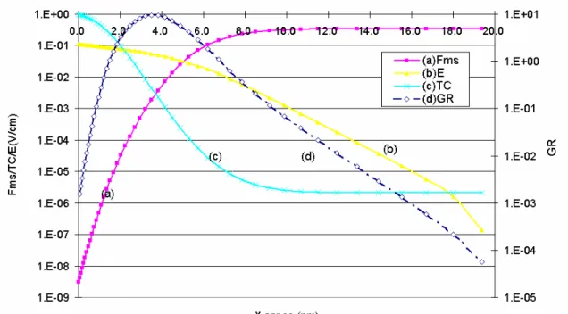
transmission coefficient, and (d) generation rate under conditions of barrier height 0.72eV and Cd 1019 c m-3 and apply voltage 0.2eV
Fig 4.3.2 Spatially distribution of (a) transition probability (b) e lectric field, (c)
transmission coefficient, and (d) generation rate under conditions of barrier height 0.72eV and Cd 1016 c m-3 and apply voltage 0.2eV
Fig 4.4.1 Current density vs apply voltage calculated by (a) Airy function s olution (b)
0.72eV and doping concentration 1019 c m-3
Fig. 4.4.2 The ratio of tunneling current, JTL to total current, J, vs apply voltage under condition of a ) Cd=1016 cm-3 b) Cd= 1019 cm-3 and barrier height 0.72eV
Fig. 4.4.3 Thermoinic -Emission current , JTE vs apply voltage, for a) Unified and b) Unity Transmission Coefficient under conditions of barrier height 0.72eV and doping concentration Cd 1016 c m-3
Fig. 4.4.4 Thermoinic-emission current vs electron energy, for a) Unified and b) Unity
Transmission Coefficient under conditions of barrier height 0.72eV and apply voltage 0.5eV and doping concentration Cd 1020 c m-3
Fig. 4.4.5 Thermoinic -emission current vs electron energy, for a) unity and b) unified
transmission coefficient under conditions of barrier height 0.72eV and apply voltage -0.5eV and doping concentration Cd 1020 c m-3
符 號 說 明
∗
m
:
effective mass of electronh
:
reduced Planck constantψ
:
wave functionAi
:
Airy function of the first kindBi
:
complementary Airy functionΓ
:
The transmission coefficientp
:
classical momentumφ
:Potential energy
m
f
:
Fermi-Dirac distribution functions in the metal
s
f
:
Fermi-Dirac distribution functions in the semiconductorΩ :atomic volume
bξ :barrier height
ms F:Transition probability
φ
∆
:
Schottky barrier lowering Xm:Interfacial layer thickness
Chapter 1 Introduction
For future design of deep sub-micron device, metal-semiconductor contact is an important consideration in the development of integrated circuit technology. It may work as a rectifying Schottky or pure ohmic contact depending on the metal work function and semiconductor impurity concentration. It is important to predict the effect of the Schottky contact on the semiconductor devices by the numerical simulation to promote the circuit development [1]. From the device design point of view, a practical and accurate model for the metal-semiconductor contact should be established.
Numerical approaches should be employed to calc ulate the electrical characteristic of metal-semiconductor contact under various conditions. The method in which only the thermionic emission at the metal-semiconductor interface is considered is simple and accurate for Schottky barrier diodes at low impurity concentrations or under low bias conditions [2]. However, it is insufficient when the tunneling phenomenon is dominated at high impurity concentration or under reverse bias. The tunneling current has been included as the current boundary condition at the metal-semiconductor interface in addition to the thermionic emission current [3,4 ]. Naturally, this method is not expected to be accurate when tunneling occurs far from the interface. Under this condition, the distribution of carriers and potential would be inaccurate in self-consistent calculations since all carriers are artificially injected at the interface. The region for calculating the tunneling current has been estimated and the carrier transport by drift and diffusion has been neglected inside the region [5,6]. This ignorance of carrier transport in the tunneling region would cause inaccuracy of potential and carrier distribution in the space charge region due to Schottky barrier.
tunneling processes are self-consistently treated with all current transport in the semiconductor. The key feature of the model is that tunneling current through the barrier is converted into a spatially distributed generation or recombination process where the local generation rate depends on the local Fermi-level at each grid and the potential profile along the tunneling path. The tunneling integral over distance and energy can be transformed into a double integral over distance alone.
The transmission coefficient of an electron through the Schottky barrier plays a key for the calculation of tunneling current. The Wentzel-Kramers -Brillouin (WKB) approximation has been widely used due to its simple mathematical form [1,7 ]. However, this approximation is not valid for the potential variation in the contact barrier is not very slowly in the general device structures. The purpose of this work is to present a more accurate numerical method to solve the Schrodinger equation in arbitrary contact potential.
Analytical solutions for Schrodinger equation exist only for some particular potential distributions such as constant potential and constant field [8,9]. Plane wave and evanescent wave solutions can be used for a step potential. The exact solution of a particle in a uniform static field can be expressed as a linear combination of Airy and complementary Airy functions.
The transfer matrix approach introduced by Tsu and Esaki [10] has been used for transmission coefficient calculation. This approach is easily extended to many layer structures with electron energy above or below the potential distribution.
The thermionic emission current can be evaluated with the calculated transmission coefficient. A unified simulation for electron transmission through the Schottky barrier is proposed in this work. The effective barrier lowering has been included in the calculation of thermionic emission current. The tunneling process is self-consistently treated with all current transport in the semiconductor [7].
In Chapter 2, several analytic solutions are introduced for transmission coefficient calculation. Single barrier is used to illuminate the Airy function and exponential function solution and then expressed in Matrix form. The electron energy over and under the barrier potential are also discussed. The traditional WKB approximation method and its limitation is explained for comparison.
In Chapter 3, some numerical simulation techniques which are used in the developed program are introduced. The space discretization concept is important for tunneling current calculation of Schottky barrier. The barrier is divided into n sections for the tunneling current calculation at each grid by transfer matrix formulation. The current density through the Schottky barrier includes the thermoinic -emission at the interface and tunneling current at bulk region. A self-consistent calculation is introduced to well link the tunneling process and thermoinic -emission process with all current transport through the Schottky barrier. The key to calculate the tunneling current through the barrier is converted into a local generation rate or recombination process which can be got by solving the device equations with boundary conditions. The barrier lowering effect is also considered with a voltage drop at the interfacial layer. The thickness of interfacial layer can be calculated for electric field calculation. The key contribution in this paper is the unified simulation for thermionic emission current calculation since the transmission coefficient can be calculated for the electron energy above the Schottky barrier.
In Chapter 4, all the simulation results and discussion are pres ented. They break into several parts in term of transmission coefficient of different transmission models , transition probability of different degeneracy models, generation rate as a function of electric field, transmission coefficient and transition probability, and unified simulation for current density through the Schottky barrier.
Chapter 2 Transmission Models
2.1 Analytic Solutions of Schrödinger Equation
The transmission of electrons through a potential barrier is usually investigated by solving the time independent Schrödinger equation:
( ) ( ) ( )
V
x
x
E
( )
x
dx
x
d
m
ψ
ψ
ψ
+
=
−
2∗ 2 22
h
(1) Where theψ
( )
x
is the wave function as a function of the positionx
,( )
x
V
is the potential distribution of the potential barrier,E
is the electron energy,∗
m
is the effective mass of electron,h
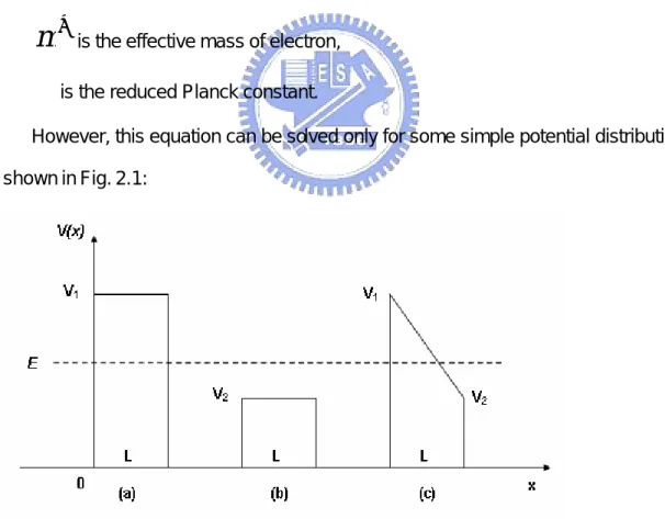
is the reduced Planck constant.However, this equation can be solved only for some simple potential distributions as shown in Fig. 2.1:
Fig. 2.1 Electron Transmission through Various Potentials
given as
V
( )
x
=
V
1, and(1) is reduced to(
)
ψ
ψ
2 1 2 22
h
E
V
m
dx
d
=
∗−
(2) The solution of this equation is( )
k
x
k
x
e
C
e
C
x
=
+
1+
−
−
1ψ
(3) Wherek
1 is the wave number given as2 1 1
)
(
2
h
E
V
m
k
=
−
∗ (4) For the barrier illustrated in Fig. 2.1(b) having the potential smaller than the electron energyV
2<
E
, the Schrödinger equation should be written as(
)
ψ
ψ
2 2 2 2*
2
h
V
E
m
dx
d
=
−
−
(5) and the corresponding solution and wave number become( )
ik x ik xe
C
e
C
x
=
+ 2+
− − 2ψ
(6) 2 2 2)
(
*
2
h
V
E
m
k
=
−
(7)For the trapezoidal barrier illustrated in Fig. 2.1(c), the potential distribution in the barrier can be expressed as
x
L
V
V
V
x
V
(
)
=
1−
1−
2 (8) Where L is the width of the trapezoidal barrier. Under this condition, the Schrödinger equation (1) can be expressed as:0
)
(
2
1 2 2 2 2=
−
−
=
∗η
ψ
ψ
x
L
V
V
m
dx
d
h
(9)Where
(
V
E
)
V
V
L
−
−
=
1 2 1η
(10) Let[
η
]
ρ
−
+
−
=
∗x
L
V
V
m
x
3 1 2 1 22
)
(
h
(11) then (9) transforms to)
(
2 2ρ
ρψ
ρ
ψ
=
d
d
(12) The typical solution to this differential equation is the Airy Function [9,11]:( )
ρ
( )
ρ
( )
ρ
ψ
=
C
+Ai
+
C
−Bi
(13) Where Ai( )
x is the Airy function of the first kind and Bi( )
x is the Airy function of second kind or complementary Airy function. The detail are described in section 3.22.2 Transfer Matrix for a Single Barrier
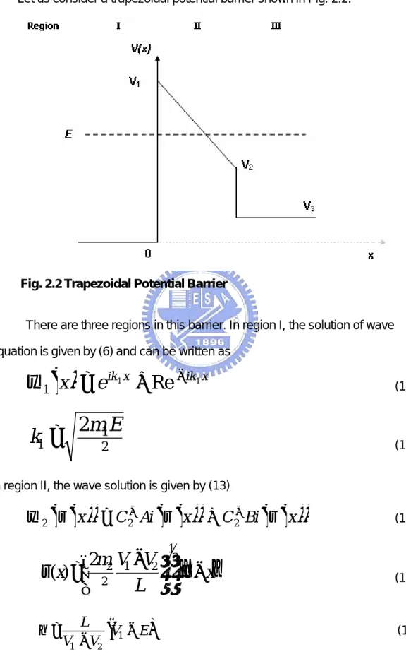
Let us consider a trapezoidal potential barrier shown in Fig. 2.2.
Fig. 2.2 Trapezoidal Potential Barrier
There are three regions in this barrier. In region I, the solution of wave equation is given by (6) and can be written as
( )
ik x ik xe
x
1Re
1 1 −+
=
ψ
(14) 2 1 12
h
E
m
k
=
(15) In region II, the wave solution is given by (13)( )
(
ρ
x
)
C
Ai
(
ρ
( )
x
)
C
Bi
(
ρ
( )
x
)
ψ
2=
2++
2− (16)[ ]
x
L
V
V
m
x
−
−
=
η
ρ
3 1 2 1 2 22
)
(
h
(17)(
V
E
)
V
V
L
−
−
=
1 2 1η
(18)In region III, we have
( )
ik
x
Te
x
33
=
ψ
(19) 2 3 3 3)
(
2
h
V
E
m
k
=
−
(20) The transfer matrix for a single barrier can be obtained by using the continuity of wave functions as well as its slope at both boundaries of the barrier. At the boundary between region I and region II, the continuity conditions are:(
(
0
)
)
(
(
0
)
)
1
+
R
=
C
2+Ai
ρ
+
C
2−Bi
ρ
(21)(
(
0
)
)
(
(
0
)
)
)
1
(
2 2 1R
C
A
i
ρ
C
B
i
ρ
ik
−
=
+′
+
−′
(22) The continuity conditions at the boundary between region II and region III are:(
L
)
C
Bi
(
L
)
T
Ai
C
2+ρ
(
)
+
2−ρ
(
)
=
(23)(
L
)
C
B
i
(
L
)
ik
T
i
A
C
2+′
ρ
(
)
+
2−′
ρ
(
)
=
3 (24) In matrix forms, (21) to (24) may be written as(
)
(
)
(
)
(
)
′
′
=
−
− + 2 2 1 1(
0
)
(
0
)
)
0
(
)
0
(
1
1
1
C
C
i
B
i
A
Bi
Ai
R
ik
ik
ρ
ρ
ρ
ρ
(25)(
)
(
)
(
)
(
)
C
ik
T
C
L
i
B
L
i
A
L
Bi
L
Ai
=
′
′
− + 3 2 21
)
(
)
(
)
(
)
(
ρ
ρ
ρ
ρ
(26) Eliminating the C2 vector from matrix equations (25) and (26), we get the transfer matrix equationT
ik
M
R
ik
ik
=
−
3 2 1 11
1
1
1
(27) where(
)
(
)
(
)
(
)
(
(
)
)
(
(
)
)
1 2)
(
)
(
)
0
(
)
0
(
−
′
′
′
′
=
Ai
Bi
Ai
L
Bi
L
M
ρ
ρ
ρ
ρ
ρ
ρ
ρ
ρ
(28)Note that this matrix is defined as the transfer matrix for region II and is a characteristic matrix for a trapezoidal barrier using the Airy function solution.
The transfer matrix for the square well using the exponential function can be derived in a similar way. For the case of an electron tunneling through a square barrier as shown Fig. 2.1 (a), we get the transfer matrix of evanescent wave solution
( )
( )
( )
( )
−
−
=
−
−
=
− − −L
k
L
k
k
L
k
k
L
k
e
k
e
k
e
e
k
k
M
L k L k L k L k 2 2 2 2 2 2 1 2 2 2 2 2cosh
sinh
sinh
1
cosh
1
1
2 2 2 2 (29)While for the case of an electron transmission o ver a square barrier as shown Fig. 2.1 (b), we get the transfer matrix of plane wave solution:
( )
( )
( )
( )
−
=
−
−
=
−
−
−
L
k
L
k
k
L
k
k
L
k
e
ik
e
ik
e
e
ik
ik
M
L
ik
L
ik
L
ik
L
ik
2
2
2
2
2
2
1
2
2
2
2
2
cos
sin
sin
1
cos
1
1
2 2 2 2 (30)2.3 Transmission Coefficients
In general, the transfer matrix eq.(27) may be written as:
T
ik
m
m
m
m
R
ik
ik
=
−
21 22 3 12 11 1 11
1
1
1
(31) Multiplying out the matrices and identifyingT
andR
as the two independent variables, we get
=
+
−
+
1 1 22 21 12 111
1
ik
R
T
ik
m
ik
m
m
ik
m
n n (32) or
+
−
−
∆
=
+
−
+
=
− 1 12 11 22 21 1 1 1 1 22 21 12 111
1
1
1
1
ik
m
ik
m
m
ik
m
ik
ik
ik
m
ik
m
m
ik
m
R
T
n n n n (33) where(
11 12)
21 22 1m
ik
m
m
ik
m
ik
+
n+
+
n=
∆
(34) Therefore, the transmissivity T and reflectivity R can be obtained as(
11 3 12)
21 3 22 1 12
m
ik
m
m
ik
m
ik
ik
T
+
+
+
=
(35)(
)
(
11 3 12)
21 3 22 1 12 3 11 1 22 3 21m
ik
m
m
ik
m
ik
m
ik
m
ik
m
ik
m
R
+
+
+
+
+
−
−
=
(36)The transmission coefficient
Γ
is defined as( )
( )
(
) (
)
2
22
3
11
1
2
12
3
1
21
2
1
2
2
m
k
m
k
m
k
k
m
k
T
E
+
+
−
=
=
Γ
(37)Square potential For V
( )
x >E( )
k
L
m
11=
cosh
2 ,( )
k
L
k
m
2 2 12sinh
1
−
=
( )
k
L
k
m
21=
−
2sinh
2 ,m
22=
cosh
( )
k
2L
The eq.(37) becomes as( )
( )
−
+
+
=
Γ
k
k
L
k
k
k
L
k
k
k
2 2 2 1 2 2 3 2 2 2 1 3sinh
cosh
1
4
1
1
(38) For E>V( )
x( )
k
L
m
11=
cos
2 ,( )
k
L
k
m
2 2 12sin
1
−
=
( )
k
L
k
m
21=
2sin
2 ,m
22=
cos
( )
k
2L
The eq.(37) becomes as( )
( )
−
+
+
=
Γ
k
k
L
k
k
k
L
k
k
k
2 2 2 1 2 2 3 2 2 2 1 3sin
cos
1
4
1
1
(39)2.4 WKB approximation for Arbitrary Potential
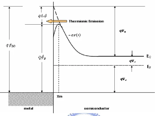
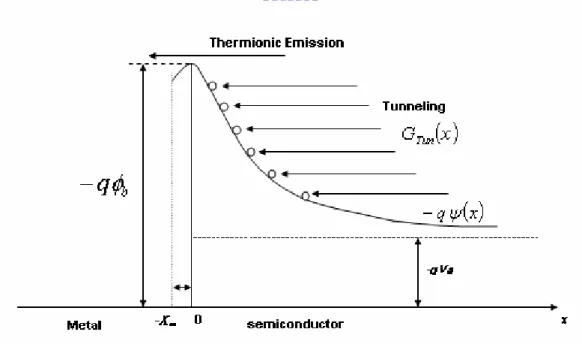
Fig. 2.4.1 Potential distribution of Schottky barrier
The WKB phase integral approximation or method is known to approximate a real Schrödinger wave function by a sinusoidal oscillation whose phase is given by the space integral of the classical momentum, the phase integral, and whose amplitude varies inversely as the fourth root of the classical momentum. This approximation was already known for the physical waves of optics and acoustics, and was quickly applied to the new Schrödinger "probability" waves.
Base on the One-dimensional time-independent Schrödinger of equation (1) And classical momentum
p
=
2
m
(
E
−
V
( )
x
)
(40) (1) can be expressed as( )
( )
x
p
dx
x
d
ψ
ψ
2 2 2 2h
−
=
(41)In semiclassical region, E>V
( )
x , p( )
x is real. Then the solution can be written in form of( ) ( )
x
A
x
[
i
φ
( )
x
]
ψ
=
exp
(42)( ) ( )
[
( )
]
( )
±
( )
=
±
=
∫
p
x
dx
x
p
C
x
x
A
x
h
1
exp
exp
φ
ψ
(43)with A
( )
x and φ( )
x are real function. The general solution of Schrödinger can be expressed in the followingWe can separate the equation into real and imaginary part. There is no general analytic solution, but ifA
( )
x varies very slowly then the A'& A'' would be very smallcompare to φ'. We can neglect the A'' to get
( )
=
p
→
=
±
∫
p
( )
x
dx
h
h
1
2 2 2 'φ
φ
(44)The transmission coefficient
Γ
can be approximated under the assumption of barrier is high or wide, V( )
x >>E, and neglecting the reflective wave. It can be written as(
2
γ
)
exp
2−
=
=
Γ
T
wherep
( )
x
dx
L∫
=
01
h
γ
, that is, (45)(
m
)
[
V
( )
x
E
]
dx
Le
∫
=
Γ
−
0−
2/
2
2
h
(46)There are some assumptions in the WKB approximation method when we got the general solution. The first one is amplitude A
( )
x variation should be small enough to make A and ' A can be ignored compare to ''φ
( )
x
. The 2nd is, it would make the WKB approximation invalid at the turning point,E
=
V
( )
x
. That is,( )
x →0p at the turning point, which is the key, make the solution turn into invalid. The 3rd is the WKB approximation neglects the reflected wave. This would make the
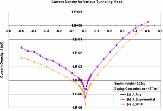
deviation of the probability compare to the numerical analysis results. The transmission coefficient is assumed to be one if the electron energy equal or above the potential dis tribution. This is used in the program to avoid the calculation problem at the turning point.
Base on the above limitation, we can see the WKB approximation to calculate the tunneling probability in Schottky Barrier as shown in Fig2.4.1, is less accuracy than other numerical methods of Airy function and exponential function solution.
Base on the description on section 2.2 and above, the transmission coefficient of the trapezoidal potential barrier is a function of electron energy, barrier width,. The
Γ
calculated by Airy function of trapezoidal barrier to electron energy, and barrier width are shown on Fig.2.5.1, and Fig.2.5.2 respectively.Fig.2.5.1 Transmission coefficient vs. electron energy by (a) Airy function (b) WKB approximation of trapezoidal barrier
Fig.2.5.2 Transmission coefficient vs. barrier width by (a) Airy function (b) WKB approximation of trapezoidal barrier
2.5 Current through the Schottky Barrier
The current through a Schottky Barrier consists of the component flowing from metal to semiconductor
J
ms and the component flowing from semiconductor to metalsm
J
. For a non-degenerated semiconductor, the current densityJ
ms is proportional to the quantum mechanical transmission coefficientΓ
( )
ξ
multiplied by the occupation probability in the metalf
m( )
ξ
and the unoccupied probability in semiconductor1
−
f
s( )
ξ
:( ) ( )
ξ
f
ξ
[
f
( )
ξ
]
d
ξ
N
qV
J
ms=
−
R c∫
∞Γ
m1
−
s 0 (47) whereV
R is the thermal velocity of electrons,N
c is the effective density of states in the conduction band, andξ
=
ε
/
k
BT
is the normalized electron energy. Similar expression forJ
sm can be expressed as( ) ( )
ξ
f
ξ
[
f
( )
ξ
]
d
ξ
N
qV
J
sm
=
R
c
∫
∞
Γ
s
1
−
m
0
(48)The total current flowing across the Schottky barrier is the sum of the above two components:
( ) ( )
ξ
[
f
ξ
f
( )
ξ
]
d
ξ
N
qV
J
=
−
R
c
∫
∞
Γ
m
−
s
0
(49)However, for heavily doped degenerated semiconductor the total current flowing from metal to semiconductor is given as:
( )
( )
( )
ξ
ξ
ξ
ξ
d
f
f
N
qV
J
m
s
c
R
Γ
−
=
∫
0
∞
ln
(50)Here
f
( )
ξ
andf
( )
ξ
are the Fermi-Dirac distribution functions in the metal andsm J
semiconductor respectively:
( )
(
)
m Fm m mf
ξ
ε
ξ
ξ
ξ
=
−
+
=
,
exp
1
1
(51)( )
(
)
n Fn n sf
ξ
ε
ξ
ξ
ξ
=
−
+
=
,
exp
1
1
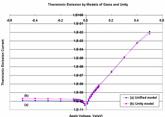
(52)For a heavily doped semiconductor or for operation at low temperatures, the Schottky barrier current given in (49) and (50) actually can be divided into two components: the quantum mechanical tunneling current
J
TL and the thermionic -emission tunneling currentJ
TE( ) ( )
ξ
ξ
ξ
ξ
d
F
N
qV
J
TL
R
c
bms
∫
Γ
−
=
0
(53)( ) ( )
ξ
ξ
ξ
ξ
F
d
N
qV
J
TE
R
c
ms
b∫
∞
Γ
−
=
(54) whereξ
b is the barrier height andF
ms( )
ξ
is the transition probability of electrons from semiconductor to meal and is given as:( )
ξ
m
( )
ξ
s
( )
ξ
ms
f
f
F
=
−
(55) for non-degenerate semiconductor and( )
( )
( )
=
ξ
ξ
ξ
m
s
ms
f
f
F
ln
(56) for degenerate semiconductor.Chapter 3 . Numerical Simulation
3.1 Space Discretization
The solutions described in Chapter 2 are base on single potential barrier. If we like to demonstrate those solutions in matrix form, the potential should be divided into small areas. Each area can be treated as single potential barrier and cascade the solution as probability and transmission coefficient calculation. There are two ways to discretized the potential barrier as shown on Fig3.1.1 by piecewise linear approximation and Fig3.1.2 by step approximation. V is the barrier height, 0 V is the a
applied voltage across the barrier. b is the width of each region. L is the total width of barrier.
Fig3.1.1 Piecewise linear approximation for Schottky Barrier. T he barrier, total depth is L, is divided into n section. S is the sth section in the barrier. The Width of each barrier is b
Fig3.1.2 Step approximation for Schottky Barrier. The barrier, total depth is L, is divided into n section. S is the sth section in the barrier. The width of each barrier is b
3.2 Transfer Matrix Formulation
In the region 0
( )
ik x ik xe
x
0Re
0 0 −+
=
Ψ
x
≤
0
(57) 2 02
h
mE
k
=
(58) In the region I( )
1 1( )
1 1( )
1 1ρ
C
Ai
ρ
C
Bi
ρ
− ++
=
Ψ
(59)( )
2
3(
1)
1 1 1 0 2 1η
ρ
−
+
−
=
x
L
V
V
m
x
h
,0
≤
x
≤
L
1 (60)(
V
E
)
V
V
L
−
−
=
0 1 0 1 1η
(61) In the region II( )
2 2( )
2 2( )
2 2ρ
C
Ai
ρ
C
Bi
ρ
− ++
=
Ψ
(62)( )
2
3(
2)
1 2 2 1 2 2η
ρ
−
+
−
=
x
L
V
V
m
x
h
, 2 1x
L
L
≤
≤
(63)(
V
E
)
V
V
L
−
−
=
1 2 1 2 2η
(64) In the region 3( )
ik xTe
x
3 3=
Ψ
, 2L
x
≥
(65) 2 3 3)
(
2
h
V
E
m
k
=
−
(66)at boundary of regions 0 and I
(
(
0
)
)
(
(
0
)
)
1
+
R
=
C
1+Ai
ρ
1+
C
1−Bi
ρ
1 (67)(
(
0
)
)
(
(
0
)
)
)
1
(
1 1 1 1 0R
C
A
i
ρ
C
B
i
ρ
ik
−
=
+′
+
−′
(68)(
)
(
)
(
)
(
)
′
′
=
−
− + 1 1 1 1 1 1 0 0(
0
)
(
0
)
)
0
(
)
0
(
1
1
1
C
C
i
B
i
A
Bi
Ai
R
ik
ik
ρ
ρ
ρ
ρ
(69) at boundary of regions I and II(
1(
1)
)
1(
1(
1)
)
2(
2(
0
)
)
2(
2(
0
)
)
1Ai
ρ
L
C
Bi
ρ
L
C
Ai
ρ
C
Bi
ρ
C
++
−=
++
− (70)(
1(
1)
)
1(
1(
1)
)
2(
2(
0
)
)
2(
2(
0
)
)
1A
i
ρ
L
C
B
i
ρ
L
C
A
i
ρ
C
B
i
ρ
C
+′
+
−′
=
+′
+
−′
(71)(
)
(
)
(
)
(
)
=
′
(
(
)
)
′
(
(
)
)
′
′
− + − + 2 2 2 2 2 2 1 1 1 1 1 1 1 1 1 1)
0
(
)
0
(
)
0
(
)
0
(
)
(
)
(
)
(
)
(
C
C
i
B
i
A
Bi
Ai
C
C
L
i
B
L
i
A
L
Bi
L
Ai
ρ
ρ
ρ
ρ
ρ
ρ
ρ
ρ
(72) at boundary of regions II and III(
L
)
C
Bi
(
L
)
T
Ai
C
2+ρ
2(
2)
+
2−ρ
2(
2)
=
(73)(
L)
C B i(
L)
ik T i A C 2+ ′ ρ 2 ( 2) + 2− ′ ρ 2 ( 2 ) = 3 (74)(
)
(
)
(
)
(
)
C
ik
T
C
L
i
B
L
i
A
L
Bi
L
Ai
=
′
′
− + 3 2 2 2 2 2 2 2 2 2 21
)
(
)
(
)
(
)
(
ρ
ρ
ρ
ρ
(75)Eliminating C1 and C2 from (69) to (72), we get
(
)
(
)
(
)
(
)
(
(
)
)
(
(
)
)
(
)
(
)
(
)
(
)
A
i
(
(
L
)
)
B
i
(
(
L
)
)
ik
T
L
Bi
L
Ai
i
B
i
A
Bi
Ai
L
i
B
L
i
A
L
Bi
L
Ai
i
B
i
A
Bi
Ai
R
ik
ik
′
′
′
′
•
′
′
′
′
=
−
− − 3 1 2 2 2 2 2 2 2 2 2 2 2 2 1 1 1 1 1 1 1 1 1 1 1 1 1 0 01
)
(
)
(
)
(
)
(
)
0
(
)
0
(
)
0
(
)
0
(
)
(
)
(
)
(
)
(
)
0
(
)
0
(
)
0
(
)
0
(
1
1
1
ρ
ρ
ρ
ρ
ρ
ρ
ρ
ρ
ρ
ρ
ρ
ρ
ρ
ρ
ρ
ρ
(76)where M1 and M2 are the transfer matrix for regions I and II
(
)
(
)
(
)
(
)
(
(
)
)
(
(
)
)
1 1 1 1 1 1 1 1 1 1 1 1 1 1)
(
)
(
)
(
)
(
)
0
(
)
0
(
)
0
(
)
0
(
−
′
′
′
′
=
L
i
B
L
i
A
L
Bi
L
Ai
i
B
i
A
Bi
Ai
M
ρ
ρ
ρ
ρ
ρ
ρ
ρ
ρ
(77)(
)
(
)
(
)
(
)
(
(
)
)
(
(
)
)
1 2 2 2 2 2 2 2 2 2 2 2 2 2 ) ( ) ( ) ( ) ( ) 0 ( ) 0 ( ) 0 ( ) 0 ( − ′ ′ ′ ′ = L i B L i A L Bi L Ai i B i A Bi Ai M ρ ρ ρ ρ ρ ρ ρ ρ (78) (76) can be expressed asT
ik
M
T
ik
M
M
R
ik
ik
=
=
−
3 3 2 1 0 01
1
1
1
1
(79) where
M
=
M
1⋅
M
2Extend to n regions as shown in chapter 3.1, the matrix o f sth region, Ms, is represented
(
)
(
)
(
)
(
)
(
(
)
)
(
(
)
)
1)
(
)
(
)
(
)
(
)
0
(
)
0
(
)
0
(
)
0
(
−
′
′
′
′
=
s s s s s s s s s s s s sL
i
B
L
i
A
L
Bi
L
Ai
i
B
i
A
Bi
Ai
M
ρ
ρ
ρ
ρ
ρ
ρ
ρ
ρ
(80) Extending to n+1 regions, we haveT
ik
M
T
ik
M
M
M
M
R
ik
ik
n n n
=
⋅⋅
⋅
=
−
1
1
1
1
1
3 2 1 0 0 (81) where∏
− = −=
=
1 2 1 3 2 n s s nM
M
M
M
M
L
(82)3.3 Discretization of Device Equations
Device Equations
The electrical properties of semiconductor device can be completely specified by physical relationship. They are 1) Poisson’ equation, 2) electron and hole transport equations, 3) Electron and hole continuity equations. Applying the boundary conditions can solve current density, electron potential, and carrier concentration. Poisson Equation
(
p
n
N
)
q
dx
d
Si+
−
−
=
ε
ψ
2 2 (83) Transport Equationsdx
dn
qD
nE
q
J
n=
µ
n x+
n (84)dx
dp
qD
pE
q
J
P=
µ
p X−
p (85) C ontinuity EquationsU
dx
dJ
q
dt
dn
n−
=
1
(86)U
dx
dJ
q
dt
dp
=
−
1
p−
(87) where n and p, Jn ad Jp, µnand µP are the concentrations, current densities, andmobility of electrons and holes, respectively. U is the recombination rate, q is the electron charge, E is the electric field, ψ is the space charge potential. ε is the Si
permittivity of semiconductor.
The main consideration in selecting a solution algorithm is the convergence properties of discretized equation and the iterative sequence. The Poisson equation is discretized and solved simultaneous with continuity equation and substituted into Transport equation to calculate the current density. The discretized procedure of
i i i i i i
p
n
N
X
X
X
X
+
∆
=
−
+
−
∆
+
∆
−
∆
+12 2 1 −111
1
ψ
ψ
ψ
(88) where(
1)
2 1 Xi Xi Xi X =∆ ∆ +∆ ∆ + and ∆X2 = ∆X+1i(
∆Xi+1+∆Xi)
2To discretized the continuity equation between the initial time t0 and final time
1
t , the equations can be written as
( ) ( )
( ) ( )
( )
( )
[
]
i n n i iG
i
x
i
x
i
J
i
J
t
t
n
t
n
+
∆
+
+
∆
−
+
+
=
∆
−
2
1
2
1
2
1
0 1 (89)( )
( )
( ) ( )
( )
( )
[
]
i p p i iG
i
x
i
x
i
J
i
J
t
t
p
t
p
+
∆
+
+
∆
−
+
+
=
∆
−
2
1
2
1
2
1
0 1 (90) The Jn of between i to i+1 section can be presented by discretized the CurrentTransport equation as
( )
( ) ( )
( )
( )
( )
(
)
(
( )
( )
( )
)
+ ∆ + − + + ∆ + − − + + + = + 1 2 1 exp 1 1 2 1 exp 1 1 2 1 2 1 2 1 i x i E i n i x i E i n i E i i J n n µ (91)3.4 Boundary Conditions
The boundary conditions of the device equations at the metal semiconductor interface are used for the thremionic emission current calculation. The barrier height,
B
φ
, including a voltage drop, ∆φ across the interfacial layer is the Schottky effect induced barrier lowering.Barrier lowering
The Schottky effect, which is the image force induced lowering of the potential energy carrier emission when an electric field