MATERIALS
CHEM;~;tYW&D
ELSEVIER Materials Chemistry and Physics 54 ( 1998) 160-163
Interfacial reactions of Ni on Si,.,,GeO~,4 and Si by pulsed laser annealing
Jian-Shing Luo ‘, Wen-Tai Lin a,*, C.Y. Chang b, W.C. Tsai b
Abstract
Pulsed KrF laser annealing and vacuum annealing on the interfacial reactions of Ni/Si,,,,Ge,,2, and NiiSi were studied. For the Nii % ,,Ge,, 21 films annealed at temperatures above 3OOT, some Ge-rich Si, _ ,Ge, grains were formed between the Ge-deficient Ni germanos- ilicide grains, resulting in the island structure. For NiiSi films homogeneous epitaxial Nisi, films could be grown even at 600°C. Ni silicide
(gerrnanosilicide j associated with the amorphous overlayer was generally formed at lowerenergy densities forNi/Si, Nisi/%, Ni/Si,,,Ge,,, and Ni( Si, -,,Ge,) /Si,,,,Ge o.zJ systems, respectively. At higher energy densities constitutional supercooling occurred. The energy densities at which constitutional supercooling appeared were higher for Nisi and Ni(Si, -,,Ge,,) than for Ni. For the continuous Ni(Si, -,,Ge,,) films grown at 200°C in a vacuum furnace, subsequent laser annealing at an energy density of 0.6-l .O J cm-’ have shown to render homogeneous Ni ( %76Ge0.24)2 and Si,,76Geo,24 films without the island structure and Ge segregation. 0 1998 Elsevier Science S.A. All rights reserved.
Keyords: Interfacial reactions: Laser annealing
1. Introduction
The Si, -,Ge,/Si heterojunction has significant potential applications in high-speed electronic and optoelectronic devices [ 1.21. Interfacial reactions of metals such as Ni [ 31, Pt [4,5], Pd [5,6], Ti [7-121 and Co [ 13-161 on Si,-,Ge, films have been studied for low-resistance ohmic contacts and as contacts for Schottky barrier infrared detectors. In these reactions the formation of a ternary phase was generally accompanied with Ge segregation. Additionally, for the Ti and Co on Si, -,Ger lilms an island structure also appeared at higher annealing temperatures [ 9.10,15.16]. These phe-
nomena are presumably ascribed to the higher heat of for-
mation for metal-Si than for metal-Ge [ 171. Rapid thermal annealing could shorten the annealing time, resulting in a
reduction of Ge segregation [9,10].
Pulsed laser annealing has been extensively used in grow- ing thin films of silicides [ 18,191: Si, -,Ge,Y [ 201, Si, -.XC, [ 2 1 ] and Si , -.r- ,.Ge&. [ 221. In comparison with furnace annealing, pulsed laser annealing offers several advantages such as much shorter operational time. confinement of the heated area without causing changes in the pre-existing struc- ture, reduction of contaminants, etc. For the growth of Si, -.YC,X and Si, -x- ,,Ge,$Z,, carbon at concentrations of some
* Corresponding author. Fax: + 886-6-2346290; E-mail: wtlin@mail. ncku.edu.tw
02.51-0584/98/$19.00 0 1998 Elsevier Science %A. AU right5 reserved.
PII SO254-0584~98~00021-8
orders of magnitude above the equilibrium solubility can be incorporated into Si and Si, -.rGe, by pulsed laser annealing due to the fast melt and resolidification process [21,22]. Similarly, it is expected that Ge segregation together with the formation of island structure, which commonly appears in the interfacial reactions of metal/Si, -.,Ge, by conventional furnace annealing, may be suppressed by pulsed laser anneal- ing. In the present study, therefore, the effort was mainly focused on studying the interfacial reactions of the Nil Si,,,,GeO,,, system as a function of the laser energy density. Meanwhile, similar studies were also carried out on the Ni/Si system for comparison.
2. Experimental
Relaxed epitaxial Si0,7hGe11.24 films about 0.15 km thick were grown on n-type ( 100) Si at 55O’C by ultra-high vacuum chemical vapor deposition. Prior to Ni deposition the sub- strates were cleaned by the RCA method and then immedi- ately loaded into the chamber. An Ni overlayer about 2.50 A
thick was deposiled on to the Sio,,hGe,,,2,/Si and Si substrates, respectively, at room temperature by electron gun evapora-
tion at a rate of 1 A s“. The base pressure was around 1 .O X 1 O-” Torr. Furnace annealing was carried out at a tem- perature of ZOO-600°C in a vacuum of 1-2X 10m6 T&r.
J.-S. Luo er 01. / Materinls Chemisrt~ and Pli,~sics 54 (1998) 160-163 161
Pulsed KrF laser annealing was performed at an energy den- sity of 0. l-l .6 J cm-’ in a vacuum around 2 X IO-’ Torr. The duration time was 14 ns. The laser beam was focused on to an area of 4 X 4 mm’. For each laser annealing the speci- men was illuminated by one shot. Phase formation, micros- tructure and chemical compositions of the reacted layer were analyzed by energy dispersive spectrometry (EDS) /trans-
mission electron microscopy (TEM) which was equipped
with a field emission gun with an electron probe 12 A in size. The variation of lattice parameters of Si,>,,,Ge,,,, films after annealing was examined by the X-ray diffraction (XRD) method with CuKa radiation. The areas of laser annealed samples used for XRD analysis were about 1 X 1 cm’, which were composed of nine adjacent 4 X 4 mm2 areas irradiated under identical conditions.
3. Results and discussion
For the Ni/Si,,,,,Ge,,,,, films annealed at a temperature of 200-SOO”C in a vacuum furnace, an Ni( Si, _ .Ge,) layer was formed, which was confirmed to be a solid solution of Nisi and NiGe by EDS/TEM analysis. From EDS/cross-sectional TEM (XTEM) analysis of the sample annealed at 300°C some Ge-rich Si, -,Ge,l grains were formed between the Ge- deficient Ni(Si, -,rGe,V) grains as shown in Fig. 1. Ge segre- gation from the Ni(Si, _ ,Ge,) layer to the Si0.,6Ge,,2a sub- strate also appeared. The heats of formation for Nisi and
NiGe have been determined to be about -45 and
- 32 kJ mol-‘, respectively [ 171. These values suggest that Ni tends to react preferably with Si. It seems that Ge is repelled from the Ni( Si, -,,Ge,) grains and diffuses into the Ni(Si, -.,Ge,) grain boundaries to react with Si and Ge from the substrate, causing the formation of the Ge-rich Si, -,yGe,, grains. Similar results have been found in the Ti/Si, -,yGe,r system by Aldrich et al. [ 9, lo]. Higher annealing tempera- tures yielded a greater Ge deficiency in the Ni(Si, -,yGe,) layer. At 400°C the Ge-rich Si, - ,Ge,y grains became con- nected, leading to the formation of the island structure. Mean- while Ge was greatly enriched in the free surface of the Sin 7hGeo.2J film. The Ni( Si, -,Ge,y) Z phase started to form at 600°C. in which only a trace amount of Ge was present.
For the Ni/S& 76Geo,24 lilms annealed at an energy density of 0.1-0.3 J cm-‘, two layers were formed on the surface of the Si0,76Geo.25 film. One example is shown in Fig. 2. From micro-diffraction analysis the upper layer was amorphous, while the lower layer was crystalline. From EDS/XTEM analysis the Ni/ (Si + Ge) atomic ratios for the upper and lower layers were about 1: 1 and 1:2, respectively. Generally, annealing at lower energy density favored the formation of an amorphous structure due to the higher cooling rate. At energy densities above 0.4 J cm-’ the constitutional super- cooling occurred, resulting in the cellular structures of Ge- deficient Si, _ ,Ge,\ island surrounded by Ni( Si, -,Ge,) 2
(b)
0.67
Fig. 1. (a) XTEM image and (b) the Ge/Si concentration ratio of an Ni/ Sh &eU 2+ film after vacuum annealing at 300°C showing that the Ge-rich Si, _ ,Ge,grains were formed between the Ge-deficientNi(Si, -,7Ge,) grains.
Fig. 2. XTEM image of an Ni/Si,,,,Ge,,, film after laser annealing at 0.3 J cm-> &owing that two layers of Ni germanosilicide were formed on the surtke of the Si,, 7hGe,j 24 film. The upper layer is amorphous, while the lower layer is crystalline.
[ 231. Poate et al. [ 181 and Tung et al. [ 191 observed the constitutional supercooling phenomenon in the Pt/Si system irradiated by Nd:YAG laser and indicated that interfacial instability and cell formation can be suppressed by melting mono- or disilicide layers.
A homogeneous Ni(Si, -,Ge,) film without the island structure could be grown at 200°C. After pulsed KrF laser annealing at an energy density of 0.6-1.2 J cm-‘, it fully transformed into a homogeneous Ni(Si,-,Ge,), film. One example of the film grown at 1 .O J cm-’ is shown in Fig. 3. It is worth noting that the island structure originally present
162 J.-S. Luo et al. /Motrricds Chemists and Phpics 54 (1998) 160-163
Fig. 3. XTEM image of an Ni/Si,,,,,Ge, 24 film after vacuum annealing at ?OOT and subbequent laser annealing at 1.0 J cmm2,
‘““I (a) S/ 200 Ni Ni 2 80 s 5 60 40 20 0 0 1 2 3 E& 5 (I& 1 8 9 10 )
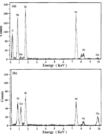
Fig. 4. EDS spectra of (a) ao NiiSi, _ ,Ge,?) grain grown at 500°C and (b) an Ni(Si,j7hGe,,24)2 film corresponding to that in Fig. 3.
in the Ni( Si,-.Ge,) films grown at temperatures above 400°C could not be removed by the subsequent laser anneal- ing. From the EDS/XTEM analysis shown in Fig. 4 it is evident that in contrast to furnace annealing, pulsed KrFlaser annealing allows a significant amount of Ge to be retained in the Ni germanosilicide, forming the Ni ( Si0.76Ge0.2d) 2 films. In the Co/Si,,,,Gec,z, system studied previously Ge segre- gation during vacuum annealing might significantly increase and decrease the c-axis lattice parameters of the upper and lower layers of the Si,,,,Ge,,,, film. respectively [ 161. In the present study, the XRD patterns in Fig. 5 show that the c-axis lattice parameter of the Si0.76Ge0,24 film after laser annealing at 1 .O J cm-’ remained nearly unchanged, revealing that Ge segregation was effectively suppressed in the Si0,76Ge0,24 film. This XRD result is consistent with the EDS/XTEM
pw.q--J
$9 ‘i!
67 68 28 (dsg)
Fig. 5. XRD patterns of the as-grown Si, -,Ge, film and the Si, -,Ge, films after annealing at various conditions.
analysis. However, the Ni concentration decreased as a func- tion of the distance from the surface of the Ni( Si,.,,Ge,,,,) 2 film. This result indicates that during one pulse irradiation, about 14 ns, the intermixing of the chemical species in the melt may not be completed due to fast resolidifica- tion. The higher Ni concentration on the surface of the Ni ( Si0_76Ge0,23)2 film is ascribed to the incomplete reaction between the Ni film and the underlying Si0,76Ge0.ZJ film dur- ing the pre-annealing at 200°C for 0.5 h in the vacuum fur- nace. The Ni(Si, -,Ge,r)z layer near the interface was epitaxially grown on the Sio.,,GeO.,, film, while part of the Ni ( Si, -,rGe1)2 layer near the surface was polycrystalline. The excess Ni on the surface of the Ni( Si0,76Ge0,23)2 film might hinder the Ni ( Si0.76Ge0.24) 2 grains from growing along the epitaxial orientations. Tung et al. [ 191 have reported similar results.
At energy densities above 1.2 J cm-’ both the Ni- (Si, -,Ge,)7 overlayer and the Si, -iGe,Y film showed Ge deficiency. An example of the Ni(Si, -rGe,Y)z films grown at 1.6 J cm-? is shown in Fig. 6. The trace of the melting depth is in the range of 0.22-0.25 pm from the film surface, which
Fig. 6. XTEM image of an Ni/Si,,7,Ge,,,, film after vacuum annealing at 200°C and subsequent laser annealing at 1.6 J cm-’ showing that the Si, _ .Ge, film grew deep into the Si substrate.
J.-S. Lm et al. / Materials Chemisr~ and Physics 54 (1998) 160-163 163
is larger than the thickness, 0.15 Frn, of the as-grown
%6Geo.24 film. From EDS/XTEM analysis the Ge concen-
tration decreased with the melting depth, indicating that the Sir -,rGe, layer penetratedly grew into the Si substrate during laser annealing. Similar results have been observed in the pulsed laser annealing of Si, -.,Ge, and Si, -x-,.GexCg films [ 22,241, At 1.6 J cm-” the cellular structure due to consti- tutional supercooling also appeared.
3.2. Ni/Si
For the Ni/Si samples annealed at 600°C homogeneous epitaxiai Nisi?_ films without the island structure wereformed.
For the Ni/Si samples irradiated at 0.4 J cm-‘the Nisi layer
associated with the amorphous overlayer was formed. From EDS/ (XTEM ) analysis the Ni:Si atomic ratio for the amor- phous overlayer was about 1: 1. At energy densities above 0.6 J cm-’ constitutional supercooling occurred.
For the Nisi films grown at 200°C subsequent laseranneal- ing at energy densities above 0.6 J cm-‘caused the formation
of homogeneous NiSiz films. From EDS/XTEM analysis the
Ni concentration decreased as a function of distance from the surface of the Nisi, film. The Nisi, layer near the interface was epitaxial, while part of the Nisi1 layer near the surface
was polycrystalline. The constitutional supercooling
appeared at 1.6 J cm-‘,
It is interesting to note that the energy densities at which constitutional supercooling occurs is much lower for Ni/Si
and Ni/Sio,7hGei),23 than for NiSi/Si and Ni(Si, -,Ge,) /
%dh2+ This result may be explained in terms of the
strong coupling of ultraviolet radiation with metals [ 251.
4. Conclusions
1. For the Ni/Si,,,,Geazj films annealed at temperatures
above 300°C some Ge-rich Si,-,Ge,r grains were formed between the Ge-deficient Ni germanosilicide, resulting in the island structure. For Ni/Si films a homogeneous epitaxial Nisi, layer could be formed even at 600°C.
2. Ni silicide (germanosilicide) associated with the
amorphous overlayer was generally formed at lower energy
densities. Constitutional supercooling occurred at higher
energy densities. The energy densities at which constitu- tional supercooling appeared were higher for NiSi/Si
and Ni( Si, -rGe.Y) /Si,,70Ge0,24 than for Ni/Si and Ni/
Sk.&e0.2+
3. For the Ni( Si, -,YGe,Y) films grown at 200°C in a vacuum furnace, subsequent laser annealing at an energy density of
Oh-I.0 J cm-’ have shown to render homogeneous
Ni ( Si,,,,Ge,,za) 2 and Si0,76Ge0.24 films without the island structure and Ge segregation.
Acknowledgements
This work was sponsored in part by the Republic of China National Science Council under Contract No. NSC-87-22 16- E-006-023. References [II r21 [31 [41 [51 [61 171 [81 191 [lOI [ItI [I21 [I31 [I41 [I51 [I61 [I71 Ltsl I191 P-01 [211 [=I [231 [241 [251
F.Y. Huang, X. Zhu, M.O. Tanner, K.L. Wang, Appl, Phys. Lett. 67 (1995) 566.
H. Presting, H. Kibbel, M. Jaros, R.M. Turton, U. Menczigar, G. Abstreiter, H.G. Grimmeiss, Semicond. Sci. Technol. 1 ( 1992) 1127. R.D. Thompson, K.N. Tu, J. Angillelo, S. Delage, S.S. Iyer; J. Elec- trochem. Sot. 135 (1988) 3161.
Q.Z. Hong, J.W. Mayer, J. Appl. Phys. 66 (1989) 611.
H.K. Liou. X. Wu, U. Gennser, V.P. Kesan, S.S. Iyer, K.N. Tu, ES. Yang, Appl. Phys. Len. 60 (1992) 577.
A. Buxbuam, M. Eizenberg, A. Raizman, F. Schaffler, Appl. Phys. Lett. 59 (1991) 665.
0. Thomas, S. Delage, F.M. d’Heurle. G. Scilla, Appl. Phys. Lett. 54 (1989) 228.
W.J. Qi, B.Z. Li, W.N. Huang, Z.G. Gu, H.Q. Lu. X.J. Zhang, M. Zhang, G.S. Dong, D.C. Miller, R.G. Aitken, J. Appl. Phys. 77 ( 1995) 1086.
D.B. Aldrich, Y.L. Chen, D.E. Sayers, R.J. Nemanich, S.P. Ashbum. M.C. Ozturk, J. Appl. Phys. 77 (1995) 5107.
D.B. Aldrich, H.L. Heck, Y.L. Chen, DE. Sayers, R.J. Nemanich, J. Appl. Phys. 78 ( 1995) 4958.
A. Eyal, R. Brener, R. Beserman, M. Eizenberg, 2. Atzmon, D.J. Smith, J.W. Mayer, Appl. Phys. Lett. 69 (1996) 64.
W. Freiman, A. Eyal, Y.L. Khait, R. Beserman, K. Dettmer, Appl. Phys. Lett. 69 (1996) 3821.
M.C. Ridgway, R.G. Elliman, N. Hauser, J.M. Baribeau, T.E. Jackman, Mater. Res. Sot. Symp. Proc. 260 (1992) 857.
F. Lin, G. sarcona, M.K. Hata1is.A.F. Cserhati,E. Austin,D.W. Greve, Thin Solid Films 250 ( 1994) 20.
Z. Wang, Y.L. Chen, H. Ying, R.J. Nemanich, D.E. Sayers, Mater. Res. Sot. Symp. Proc. 320 (1991j 397.
J.S. Luo, W.T. Lin, C.Y. Chang, W.C. Tsai, S.J. Wang, Mater. Chem Phys. (1997) 140.
F.R. Deboer, R. Boom, W.C. Mattens, A.R. Miedema, A.K. Niessen (Eds.), Cohesion in Metals: Transition Metal Alloys, North Holland, Amsterdam, 1988.
J.M. Poate, H.J. Leamy, T.T. Sheng, G.K. Celler, Appl. Phys. Lett. 33 (1975) 918.
R.T. Tung, J.M. Gibson, DC. Jacobson, J.M. Poate, Appl. Phys. Lett. 43 (1983) 476.
J.R. Abelson, T.W. Sigmon, K.B. Kim, K.H. Weiner, Appl. Phys. Lett. 52 (1988) 230.
Z. Kantor, E. Fogarassy, A. Grob, J.J. Grab, D. Muller, B. Prevot, R. Stuck, Appl. Phys. Lett. 69 (1996) 969.
J. Boulmer, P. Boucaud, C. Guedj, D. Debarre, D. Bouchier, E. Finkman, S. Prawer, K. Nugent, A. Desmur-Larre, C. Godet, P.R. Cabarrocas, J. Cryst. Growth 157 (1995) 436.
J.S. Luo, W.T. Lin, C.Y. Chang, W.C. Tsai, J. Appl. Phys. 82 (1997) 364.
F. Replinger, E. Fogarassy, A. Grob, J.J. Grab, D. Muller, B. Prevot, J.P. Stoquert, S.D. Unamuno, Thin Solid Films 241 (1994) 155. E. D’Anna, G. Leggieri, A. Luches. Appl. Phys. A 45 (1988) 325.