A simple method to characterize the afterpulsing effect in single photon avalanche
photodiode
H. T. Yen, S. D. Lin, and C. M. Tsai
Citation: Journal of Applied Physics 104, 054504 (2008); doi: 10.1063/1.2968434
View online: http://dx.doi.org/10.1063/1.2968434
View Table of Contents: http://scitation.aip.org/content/aip/journal/jap/104/5?ver=pdfcov Published by the AIP Publishing
Articles you may be interested in
Photon-number resolving performance of the InGaAs/InP avalanche photodiode with short gates Appl. Phys. Lett. 95, 131118 (2009); 10.1063/1.3242380
Practical fast gate rate InGaAs/InP single-photon avalanche photodiodes Appl. Phys. Lett. 95, 091103 (2009); 10.1063/1.3223576
Free-running In Ga As In P avalanche photodiode with active quenching for single photon counting at telecom wavelengths
Appl. Phys. Lett. 91, 201114 (2007); 10.1063/1.2815916
Differential phase shift quantum key distribution using single-photon detectors based on a sinusoidally gated In Ga As In P avalanche photodiode
Appl. Phys. Lett. 91, 011112 (2007); 10.1063/1.2753767
Numerical analysis of single photon detection avalanche photodiodes operated in the Geiger mode J. Appl. Phys. 99, 124502 (2006); 10.1063/1.2207575
A simple method to characterize the afterpulsing effect in single photon
avalanche photodiode
H. T. Yen, S. D. Lin,a兲and C. M. Tsai
Department of Electronic Engineering, National Chiao Tung University, 1001 Ta Hsueh Road, Hsinchu 300, Taiwan
共Received 17 January 2008; accepted 13 June 2008; published online 3 September 2008兲
A simple method is introduced for studying the afterpulsing effect in InGaAs single photon avalanche photodiode. The afterpulsing probability is obtained through measuring the detection efficiencies of various biasing pulses, while the incident photons are kept constant. The effect of excess bias and temperature on the afterpulsing probability is investigated. When the device temperature is higher than 170 K, the afterpulsing probability is lower than 5% for all excess bias voltages because the trapped carrier lifetime is much shorter than the repetition period. © 2008
American Institute of Physics.关DOI:10.1063/1.2968434兴
I. INTRODUCTION
Single photon detectors are widely applied to ultralow power light detection and ultrafast optical measurement. The performance of single photon detection has made significant progress recently as a result of the growing demands in quan-tum cryptography, time resolved photoluminescence, and as-tronomical photometry.1,2Early single photon detection sys-tems utilized photomultiplier tubes 共PMTs兲 to detect single photons. The PMT has been gradually replaced by single photon avalanche photodiodes共SPADs兲 for single photon de-tection lately due to their high bias operation and low detec-tion efficiency. Currently, the silicon 共Si兲 SPAD has high detection efficiency共⬃70%兲, low dark count probability, and extremely weak afterpulsing effect at room temperature so it has been used for detecting single photons with wavelength below 1 m. Meanwhile, the InGaAs SPAD attracts increas-ing attention owincreas-ing to its ability of detectincreas-ing sincreas-ingle photons within the range of 1.3– 1.55 m, which is essential for a fiber-based long-distance quantum communication. How-ever, the applications of InGaAs SPAD are limited by its serious afterpulsing effect.3–6
When an avalanche photodiode 共APD兲 is operating in the Geiger mode, in which the bias across the APD is above its breakdown voltage, the electric field in avalanche region is so high that the breakdown current can be triggered by a single carrier. The amount of triggered output current de-pends on the excess voltage rather than on the incident pho-ton numbers. Therefore, the power level of incident light is obtained with SPAD through counting of breakdowns. In or-der to have the SPAD breakdown sequentially for repetitive photon counting, the SPAD has to be shutdown after the breakdown is triggered and then it has to be restored for the next photon detection. At present, there are three methods of turning a SPAD off: passive quenching,7active quenching,8,9 and operating in gated mode.4 In passive quenching, one serially connects the SPAD with a large resistor that dismem-bers the voltage drop when the macroscopic共about tenths of
microamperes兲 breakdown current is triggered thus the SPAD turns off automatically afterward. The active quench-ing implements an active circuit to lower the bias below the breakdown voltage for a short period of time after the trigger event. In the operation of gated mode, a pulsed voltage source is supplied to the SPAD to keep its bias above the breakdown voltage for a very short period of time and hence the SPAD can be triggered by a single carrier. That is par-ticularly useful for the detection of repetitive single photons because one can minimize the detection period to suppress the dark count as well as to maintain the detection efficiency through synchronizing the incoming photons. Hence, the gated mode is widely used in the quantum communication.
To characterize the afterpulsing effect of InGaAs SPAD in the gated mode, one usually uses a time-delay method.4 This method is complicated with its setup and not compatible with the conventional measurement of the SPAD’s perfor-mance, such as dark count probability and detection effi-ciency. This makes it difficult to optimize the performance and, at the same time, to minimize the afterpulsing counts. In this report, we propose and demonstrate a method, which is easy to operate and is compatible with the performance char-acterization, to study the afterpulsing effect in the InGaAs SPAD.
II. EXPERIMENT RESULTS AND DISCUSSION A. Measurement setup
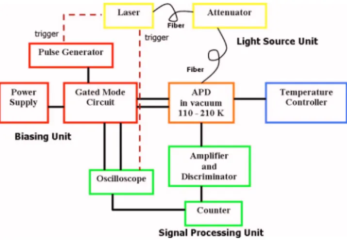
In this work, an InGaAs APD manufactured by NEC 共Product No. NR8300兲 is used. The setup system consists of three units 共the biasing, signal processing, and light source units兲 and one device test chamber, as shown in Fig.1. The biasing unit supplies the bias voltage to operate the APD in the gated mode. The unit is composed of a dc bias source 共Keithley 230兲 and a pulse generator 共HP 8114A兲. The signal processing unit, which includes a discriminator, a voltage amplifier, and a counter, processes the output signal of the APD. The discriminator and the amplifier are combined in a photocounting module and the counter comes from the Stan-ford Research System 共SR400兲. In the light source unit, a a兲Author to whom correspondence should be addressed. Electronic mail:
sdlin@mail.nctu.edu.tw.Tel.:⫹886–3-5131240. FAX: ⫹886-3-5724361.
0021-8979/2008/104共5兲/054504/4/$23.00 104, 054504-1 © 2008 American Institute of Physics
1.3 m pulsed laser共pulse width ⬃25 ps兲 with tunable rep-etition period is used. To avoid emitting two photons in one pulse, we set the output power at the level of 0.1 photon/ pulse. The output power is measured by a power meter at a few nanowatts and then lowered down to 0.1 photon/pulse in average 共⬃10−13 W兲 by a calibrated attenuator. The APD under test is cooled with liquid nitrogen and its temperature is controlled by a heating resistor. In order to synchronize the incident photons and the detection period, we connect the biasing and the light source units with a triggering signal and use a delay generator to compensate the delay time.
Typical measured waveforms are shown in Fig.2. The bias voltage across the APD is, most of time, about 2 V below the breakdown voltage but goes over the breakdown voltage about 2.5 V共excess voltage兲 in a very short period of about 40 ns in which the APD can be triggered by single carriers in its avalanche region. As the current output wave-form shown in Fig. 2, the SPAD is not triggered in each period even when the bias voltage is higher than its break-down voltage. It clearly demonstrates the bistable current-voltage characteristic of the SPAD.1On the other hand, be-cause the output current is not turned off before the end, the times of breakdown cannot be larger than one in each period. Accordingly, we calculate the triggered events by counting the number of periods in which the breakdown happens.
B. Results and discussions
The dark counts in a SPAD have two major origins: ther-mal and trap-released carriers. Therther-mal carriers caused by thermal excitation can trigger breakdown without any incom-ing photons and hence make wrong counts. These carriers can be largely suppressed by cooling down the SPAD. The trap-released carriers come from the previous breakdown events. When the breakdown happens, enormous carriers are generated and then the trapping centers are filled. The trapped carriers are released after a period of time 共trapped carrier lifetime兲. If the trapped carrier lifetime is comparable to or larger than the repetition period, the released carriers may trigger breakdown events during the subsequent detec-tion periods so that the dark count rate will increase and/or the photon count will be overestimated. This is known as afterpulsing effect. The afterpulsing effect can be eliminated by decreasing the repetition rate of detection. If the repetition period is much longer than the trapped carrier lifetime, the trapped carriers will be totally released in the off time of SPAD. However, longer repetition period means lower detec-tion efficiency so that an optimizadetec-tion of the repetidetec-tion rate is necessary to improve the performance of SPAD.
The dark count probabilities at each repetition period were measured at various temperatures, as shown in Fig.3. At the repetition period of 10 s, the dark count probability increases as the temperature increases because the higher temperature excites more dark carriers. However, as the rep-etition period becomes shorter, the dark count probability at 110 K grows dramatically. It is even higher than that at 230 K when the repetition period is 1 s. This is reasonable if we consider the contribution of afterpulsing effect. The trapped carrier lifetime becomes longer as the temperature drops. At 110 K, the dark count contributed from the after-pulsing effect is negligible at the repetition period of 10 s but it becomes dominant at 1 s. The fact tells us that the trapped carrier lifetime is around a few microsecond. For a higher temperature, e.g., at 230 K, the trapped carrier life-time becomes so short such that the measured dark count probabilities are nearly constant at all repetition periods.
As we have seen in the measurement of dark count prob-ability, a lower temperature can suppress the dark count due to thermal carriers but, at the same time, it increases the FIG. 1. 共Color online兲 The system setup for single photon detection.
FIG. 2. 共Color online兲 Measured waveforms of the bias voltage and the output current of a SPAD.
FIG. 3.共Color online兲 Measured dark count probabilities at 40 ns detection width with various repetition periods and temperatures.
054504-2 Yen, Lin, and Tsai J. Appl. Phys. 104, 054504共2008兲
afterpulsing counts from trapped carriers. In order to opti-mize the performance of SPAD, we introduce a quantitative method to characterize the afterpulsing effect under various conditions. The afterpulsing effect is governed by Eq. 共1兲 below.5 The average released carriers 共Nr兲 within the
dura-tion time of detecdura-tion width共⌬t兲 is proportional to the aver-age trapped carrier共Ntrap兲 in one breakdown and to the dark count probability共Pd兲. It also largely depends on the
repeti-tion period 共T兲 and trapped carrier lifetime 共兲. Unsurpris-ingly, a longer repetition period or shorter detection width gives less released carriers as well as weaker afterpulsing effect, according to Eq.共1兲, which is as follows:
Nr= PdNtrap exp
冉
⌬t 冊
− 1 exp冉
T 冊
− 1 . 共1兲In conventional measurements, the afterpulsing probabil-ity is defined as the probabilprobabil-ity of a breakdown that triggers another breakdown afterwards in a detection width⌬t and a repetition period T. According to Eq.共1兲, we can vary either the repetition period T or the detection width ⌬t to extract the afterpulsing probability because the Pd, Ntrap, and are usually constant at a fixed temperature. In our method, with the consideration of simplicity, we fixed the T and analyzed the afterpulsing probability at various⌬t. Figure4 schemati-cally shows our measurement method. At a fixed tempera-ture, excess bias, and repetition period, the detection effi-ciencies of two detection widths 共intervals A and B兲 were obtained with a constant incoming photon number in interval
A. We can ensure that there is no additional photon coming
into interval B by synchronizing the incoming photons with the detection pulse. Therefore, there should have no addi-tional events detected in interval B if there is no afterpulsing effect. By means of calculating the differences of detection efficiencies between two intervals, we can establish the af-terpulsing probability in the difference interval between in-tervals A and B. The validity of our method is revealed in the following equations:
DEA= Csignal
Nph
DEB=
Csignal⫻ 共1 + APPB−A兲 Nph , 共2兲 APPB−A= 共DEB− DEA兲 ⫻ Nph Csignal =DEB− DEA DEA . 共3兲
The notations are as follows: DEA共DEB兲–the detection
efficiency measured with interval A 共B兲; Csignal—the signal count measured with interval A, Nph—the number of incident photons in interval A, and APPB−A—the afterpulsing
prob-ability in the difference interval between intervals A and B. If the power of incident light in interval A共Nph兲 and the excess bias are fixed, the numbers of breakdown triggered by in-coming photons will keep constant in different detection widths. In other words, the Csignal will be the same for the measurements of DEA and DEB. Accordingly, we can obtain
the APPB−A in Eq. 共3兲 merely through measuring the DEA
and DEB in Eq.共2兲. The afterpulsing probabilities in various
conditions, e.g., temperatures, repetition periods, and excess bias, can be extracted and discussed in a quantitative way.
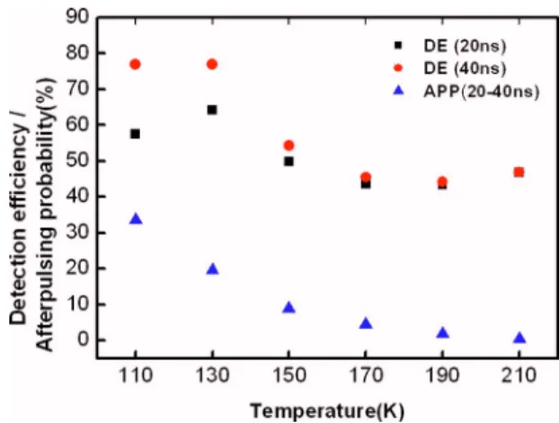
A typical measurement of the afterpulsing effect is shown in Fig. 5. The detection widths of intervals A and B were 20 and 40 ns. The repetition period was 10 s and the excess bias was 3.5 V at all temperatures. The difference of detection efficiencies between 20 and 40 ns detection widths is significant at low temperatures 共110–150 K兲 but ap-proaches to zero at high temperatures 共170–210 K兲. Using Eq. 共3兲, the calculated afterpulsing effect is also plotted in Fig.5. It is clear that the afterpulsing probability decreased as the temperature increased. This can be understood by not-ing that the trap carrier lifetimes are shorter at higher tem-peratures, so the afterpulsing effect is weakened at fixed rep-etition period, according to Eq. 共1兲. The temperature dependence of afterpulsing is similar to reported literatures,10–12 which confirm the validity of our scheme. However, a quantitative comparison is difficult as the after-pulsing effect is strongly dependent on the epitaxial struc-ture, crystal quality, and device processing, so it varies from device to device.11
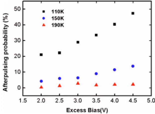
With the same method, we have also studied the influ-ence of excess bias on the afterpulsing effect. The afterpuls-ing probabilities at 110, 150, and 190 K with a repetition period of 10 s are shown in Fig.6. We can see that, in the extreme case, the afterpulsing probability goes up to nearly 50% at 110 K with the excess bias of 4.5 V. Higher excess FIG. 4.共Color online兲 A schematic figure of our measurement method for
analyzing the afterpulsing effect. Intervals A and B have different detection widths and the photons are synchronized and kept in the common interval A.
FIG. 5. 共Color online兲 Measured detection efficiencies at 20 and 40 ns detection widths and the calculated afterpulsing probabilities.
bias enhances the afterpulsing effect because more carriers are generated and trapped. Furthermore, the afterpulsing probabilities at high temperatures are largely suppressed at all excess bias voltages, as the trapped carrier lifetime be-comes much shorter than the repetition period at high tem-peratures. Based on the above, the optimization of the SPAD performance was achieved under the following conditions:
T = 170– 210 K, repetition period =10 s, and detection width =20 ns. The afterpulsing probability was lower than 5%, and the detection efficiency and the dark count probabil-ity were compromised to get the lowest noise equivalent power 共NEP兲. As a result, the best performance of the In-GaAs SPAD is 57% detection efficiency with a dark count probability of 1.2%, which has been obtained with 4.5 V excess bias and 20 ns detection width at 190 K. The calcu-lated NEP is 7⫻10−16 W/Hz1/2.
III. CONCLUSION
We propose and demonstrate a simple method to charac-terize the afterpulsing effect in various conditions. The
after-pulsing probability can be obtained through measuring the detection efficiencies at different detection widths provided that the synchronized incident photons are kept constant. We have found that the afterpulsing probabilities are less than 5% when the temperature is higher than 170 K. The best performance without the afterpulsing counts is 57% detec-tion efficiency with 1.2% dark count probability. The corre-sponding NEP is 7⫻10−16 W/Hz1/2.
ACKNOWLEDGMENTS
This work was financially supported by the National Sci-ence Council of Taiwan under Contract Nos. NSC 96-2221-E-009-218 and 96-2120-M-009-010. The authors appreciate Dr. Pan in Truelight Inc. for his kind help with the device package. S.D.L. thanks P. L. Tang for her kind help.
1S. Cova, M. Ghioni, A. Lotito, I. Rech, and F. Zappa,J. Mod. Opt.51,
1267共2004兲.
2M. Liu, X. Bai, C. Hu, X. Guo, J. C. Campbell, Z. Pan, and M. M.
Tashima, IEEE Photonics Technol. Lett. 19, 378共2007兲.
3P. Hiskett, G. Buller, A. Loudon, J. Smith, I. Gontijo, A. Walker, P.
Townsend, and M. Robertson,Appl. Opt.39, 6818共2000兲.
4G. Ribordy, J. Gautier, H. Zbinden, and N. Gisin,Appl. Opt.37, 2272
共1998兲.
5Y. Kang, H. X. Lu, Y.-H. Lo, D. S. Bethune, and W. P. Risk,Appl. Phys. Lett.83, 2955共2003兲.
6S. J. Fancey, G. S. Buller, J. S. Massa, A. C. Walker, C. J. McLean, A.
McKee, A. C. Bryce, J. H. Marsh, and R. M. De La Rue,J. Appl. Phys.79,
9390共1996兲.
7R. G. Brown, K. D. Ridley, and J. G. Rarity, Appl. Opt. 25, 4122共1986兲. 8R. G. Brown, R. Jones, J. G. Rarity, and K. D. Ridley, Appl. Opt. 26, 2383
共1987兲.
9F. Zappa, M. Ghioni, S. Cova, C. Samori, and A. C. Giudice,IEEE Trans. Instrum. Meas.49, 1167共2000兲.
10X. Jiang, M. A. Itzler, R. Ben-Michael, K. Slomkowski, M. A. Krainak, S.
Wu, and X. Sun, IEEE J. Quantum Electron. 44, 3共2008兲.
11M. A. Itzler, R. Ben-Michael, C. F. Hsu, K. Slomkowski, A. Tosi, S. Cova,
F. Zappa, and R. Ispasoiu,J. Mod. Opt.54, 283共2007兲.
12K. E. Jensen, P. I. Hopman, E. K. Duerr, E. A. Dauler, J. P. Donnelly, S.
H. Groves, L. J. Mahoney, K. A. McIntosh, K. M. Molvar, A. Napoleone, D. C. Oakley, S. Verghese, C. J. Vineis, and R. D. Younger,Appl. Phys. Lett.88, 133503共2006兲.
FIG. 6. 共Color online兲 The afterpulsing probabilities obtained at various excess bias voltages at 110, 150, and 190 K.
054504-4 Yen, Lin, and Tsai J. Appl. Phys. 104, 054504共2008兲