Vertical-cavity and randomly scattered lasing
from different thicknesses of epitaxial ZnO films
grown on Y
2
O
3
-buffered Si (111)
C. C. Kuo,1 W.-R. Liu,2 B. H. Lin,1,2 W. F. Hsieh,1,* C.-H. Hsu,2 W. C. Lee,3 M. Hong,4 and J. Kwo5
1Department of Photonics & Institute of Electro-Optical Engineering National Chiao Tung University, 1001 Tahsueh
Rd., Hsinchu 30010, Taiwan
2National Synchrotron Radiation Research Center, Hsinchu 30076, Taiwan
3Department of Materials Science and Engineering, National Tsing Hua University, Hsinchu 30013, Taiwan 4Graduate Institute of Applied Physics and Department of Physics, National Taiwan University, Taipei 10617,
Taiwan
5Department of Physics, National Tsing Hua University, Hsinchu 30013, Taiwan 2[email protected]
Abstract: Two different types of lasing modes, vertical Fabry-Perot cavity
and random lasing, were observed in ZnO epi-films of different thicknesses grown on Si (111) substrates. Under optical excitation at room temperature by a frequency tripled Nd:YVO4 laser with wavelength of 355 nm, the lasing thresholds are low due to high crystalline quality of the ZnO epitaxial films, which act as microresonators. For the thick ZnO layer (1,200 nm), its lasing action is originated from the random scattering due to the high density of crack networks developed in the thick ZnO film. However, the low crack density of the thin film (555 nm) fails to provide feedback loops essential for random scattering. Nevertheless, even the lower threshold lasing is achieved by the Fabry-Perot cavity formed by two interfaces of the thin ZnO film. The associated lasing modes of the thin ZnO film can be characterized as the transverse Gaussian modes attributed to the smooth curved surfaces.
©2013 Optical Society of America
OCIS codes: (140.3610) Lasers, ultraviolet; (140.5960) Semiconductor lasers; (160.4236)
Nanomaterials; (160.4760) Optical properties
References and Links:
1. J. C. Johnson, H.-J. Choi, K. P. Knutsen, R. D. Schaller, P. Yang, and R. J. Saykally, “Single gallium nitride nanowire lasers,” Nat. Mater. 1(2), 106–110 (2002).
2. R. M. Ma, X. L. Wei, L. Dai, S. F. Liu, T. Chen, S. Yue, Z. Li, Q. Chen, and G. G. Qin, “Light coupling and modulation in coupled nanowire ring-Fabry-Pérot cavity,” Nano Lett. 9(7), 2697–2703 (2009).
3. P. Yang, H. Yan, S. Mao, R. Russo, J. Johnson, R. Saykally, N. Morris, J. Pham, R. He, and H. J. Choi, “Controlled growth of ZnO nanowires and their optical properties,” Adv. Funct. Mater. 12(5), 323 (2002). 4. M. H. Huang, S. Mao, H. Feick, H. Yan, Y. Wu, H. Kind, E. Weber, R. Russo, and P. Yang, “Room-temperature
ultraviolet nanowire nanolasers,” Science 292(5523), 1897–1899 (2001).
5. M. A. Versteegh, D. Vanmaekelbergh, and J. I. Dijkhuis, “Room-temperature laser emission of ZnO nanowires explained by many-body theory,” Phys. Rev. Lett. 108(15), 157402 (2012).
6. H. Cao, Y. G. Zhao, S. T. Ho, E. W. Seelig, Q. H. Wang, and R. P. H. Chang, “Random laser action in semiconductor powder,” Phys. Rev. Lett. 82(11), 2278–2281 (1999).
7. S. F. Yu, C. Yuen, S. P. Lau, W. I. Park, and G.-C. Yi, “Random laser action in ZnO nanorod arrays embedded in ZnO epilayers,” Appl. Phys. Lett. 84(17), 3241 (2004).
8. H. C. Hsu, C. Y. Wu, and W. F. Hsieh, “Stimulated emission and lasing of random-growth oriented ZnO nanowires,” J. Appl. Phys. 97(6), 064315 (2005).
9. Y. T. Chen and Y. F. Chen, “Enhanced random lasing in ZnO nanocombs assisted by Fabry-Perot resonance,” Opt. Express 19(9), 8728–8734 (2011).
10. X. Ma, P. Chen, D. Li, Y. Zhang, and D. Yang, “Electrically pumped ZnO film ultraviolet random lasers on silicon substrate,” Appl. Phys. Lett. 91(25), 251109 (2007).
11. E. S. P. Leong, S. F. Yu, and S. P. Lau, “Directional edge-emitting UV random laser diodes,” Appl. Phys. Lett.
12. S. Kalusniak, H. J. Wünsche, and F. Henneberger, “Random semiconductor lasers: scattered versus Fabry-Perot feedback,” Phys. Rev. Lett. 106(1), 013901 (2011).
13. W.-R. Liu, Y.-H. Li, W. F. Hsieh, C.-H. Hsu, W. C. Lee, Y. J. Lee, M. Hong, and J. Kwo, “Domain matching epitaxial growth of high-quality ZnO film using a Y2O3 buffer layer on Si (111),” Cryst. Growth Des. 9(1), 239 (2009).
14. Y. F. Huang, S. Chattopadhyay, Y. J. Jen, C. Y. Peng, T. A. Liu, Y. K. Hsu, C. L. Pan, H. C. Lo, C. H. Hsu, Y. H. Chang, C. S. Lee, K. H. Chen, and L. C. Chen, “Improved broadband and quasi-omnidirectional anti-reflection properties with biomimetic silicon nanostructures,” Nat. Nanotechnol. 2(12), 770–774 (2007). 15. B. H. Lin, W. R. Liu, S. Yang, C. C. Kuo, C.-H. Hsu, W. F. Hsieh, W. C. Lee, Y. J. Lee, M. Hong, and J. Kwo,
“The growth of an epitaxial ZnO film on Si(111) with a Gd2O3(Ga2O3) buffer Layer,” Cryst. Growth Des. 11(7), 2846–2851 (2011).
16. J. F. Muth, R. M. Kolbas, A. K. Sharma, S. Oktyabrsky, and J. Narayan, “Excitonic structure and absorption coefficient measurements of ZnO single crystal epitaxial films deposited by pulsed laser deposition,” J. Appl. Phys. 85(11), 7884 (1999).
17. E. S. P. Leong and S. F. Yu, “UV Random lasing action in p-SiC(4H)/i-ZnO–SiO2 nanocomposite/n-ZnO:Al heterojunction diodes,” Adv. Mater. (Deerfield Beach Fla.) 18(13), 1685–1688 (2006).
18. J. T. Verdeyen, Laser Electronics (3rd ed. Prentice Hall, 1995).
19. W.-R. Liu, W. F. Hsieh, C.-H. Hsu, K. S. Liang, and F. S.-S. Chien, “Threading dislocations in domain-matching epitaxial films of ZnO,” J. Appl. Cryst. 40(5), 924–930 (2007).
1. Introduction
In the past decades, random lasing (RL) and Fabry-Perot (FP) lasing of semiconductor nanostructures have received extensive investigations by both experiment and theory for their importance and promising applications in solid-state laser. The nano-sized materials function as both gain mediums and optical resonant cavities without external mirrors for supporting essential feedback. Random and standard FP cavities are the most common and simple optical cavity structures, which can effectively lower lasing threshold. For nano-sized FP optical cavities, the well-defined two-end faces of the gain medium act as two reflecting mirrors and provide the photon feedback required for the realization of lasing. FP lasing had been successfully achieved in many semiconductor nanostructures such as GaN, CdS, and ZnO nanowires [1–5]. RL action is not achieved by an external resonator but by multiple scatterers distributed randomly in a gain medium or which by themselves act as optical amplifiers. RL phenomena have been demonstrated in nanopowders [6], nanowires [7,8], nanocombs [9], and thin film structures [10,11]. The lasing mechanisms of the RL and FP lasing employ not only the gain material but also the self-contained optical cavity via interface scattering or reflection, and thus the two kinds of lasing actions should happen simultaneously in the nanostructures.
In the microresonators fabricated by the ZnCdO/ZnO quantum well structures, Kalusniak, et al. [12] have investigated the lasing actions of FP and RL simultaneously resulting from cavity and scattered feedbacks. They reported the pure RL often requires a larger gain than the FP lasing, even though only the relatively small natural facet reflectivity is utilized in the FP microcavity with the existence of large excitonic gain of ZnO-based material. Their theoretical analysis considered the influence of different sizes of scattering center and FP feedback with scattering influences on lasing threshold. The results reveal that with the increasing scattering size in the microcavities, the lasing threshold of FP increases slightly but for RL the threshold decreases significantly. The two kinds of lasing mechanisms, RL and FP lasing actions, can exist simultaneously, when the multiple scattering and two-end faces
2. Experiments
High quality c-plane ZnO epitaxial films were grown by pulsed-laser deposition on Si(111) substrates with a 9 nm thick Y2O3 buffer layer, which was grown by electron beam evaporation. The details of the sample preparation have been published elsewhere [13]. Micro-photoluminescence (micro-PL) spectra of the ZnO epitaxial films were measured using the third harmonic of a Nd: YVO4 laser (at 355 nm) as the excitation source with a pulse width of 500 ps and repetition rate of 1 kHz. The excitation laser beam was directed normally to the sample and focused onto its surface with the power adjustable with an optical attenuator. The spectra of spontaneous and stimulated emissions were collected by a fiber bundle, which is coupled to a Triax-320 monochromator equipped with an electrically cooled charge-coupled device (CCD). And a beam profiler is used to record the profiles of lasing emissions. All the measurements were done normal to the sample surfaces and three different pumping areas, 1.13 × 10⁻⁴, 7.85 × 10⁻⁵, and 5.03 × 10⁻⁵ cm2 were adopted. An optical microscope was used to observe the micro-cracks of the films. A scanning electron microscopy (SEM) was employed to measure the film thickness and surface roughness. All the experiments were performed at room temperature.
3. Results and discussion
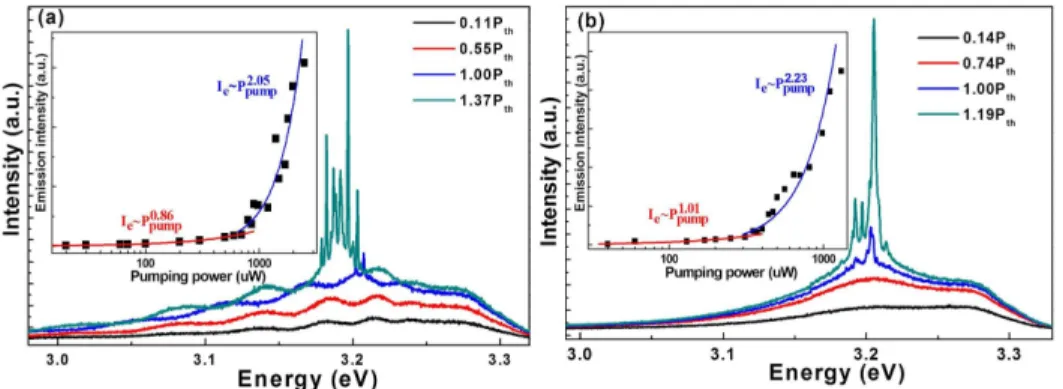
To explore the lasing properties of ZnO epi-films of different microstructures, the micro-PL spectra of two samples with thickness around 1,200 (the thick film) and 555 nm (the thin film) are measured as a function of pump-power (Fig. 1). At low pumping, all the spectra show broad emission with modulated ripples indicating interference fringes, which are originated from the structure resonance formed between the top and bottom interfaces of the films due to the high reflectance (> 50%) of Si wafer in the ultraviolet (UV) range [14] and the smooth ZnO surface. With increasing pumping intensity, many narrow emission lines with linewidth ~1.45 meV emerge around 3.2 eV, the low-energy part of the near-band edge (NBE) emission band. The emission spectra were decomposed into a broad spontaneous emission and sharp peaks. The insets in Fig. 1 illustrate the emission intensity (Ie) versus the pumping power (Ppump) plot on a log-log scale as well as the fittings by a power law. The red lines are the fittings to the spontaneous emission, of which the slopes are close to 1. The blue-lines, which present the fittings to the stimulated emissions, have slopes larger than 2. For both samples, the excited intensities of the broad spontaneous emission increase almost linearly with the pumping intensity; however, the intensities of the narrow peaks exhibit a nonlinear dependence on the excitation intensity. For both samples, the emission is dominated by the broad spontaneous emission below the lasing threshold Pth, which is defined as the intersect of the blue line to the abscissa at Ie = 0; above which the stimulated emission grows rapidly. The spectra also show progressive red shift with rising pumping power, which is attributed to local heating by the excited laser beam. The lasing thresholds are determined to be 1,200 and 920 W/cm2 with power slopes of 2.05 and 2.23 for the thick and thin samples, respectively. The observed low lasing thresholds may be attributed to the high crystalline quality of the ZnO layers and the Si has better thermal conductivity than sapphire to reduce the thermal effects effectively.
Fig. 1. Pumping power dependent lasing spectra of the ZnO epi-layers with thicknesses of (a) 1,200 nm and (b) 555 nm grown on Si(111). The insets show the corresponding linear scale plots of emission intensity versus pumping power.
As aforementioned, the lasing action in ZnO nanostructures can involve two kinds of lasing mechanisms. A single-crystal nanostructure of ZnO is a gain medium by itself and can also function as a natural FP cavity formed between the two-end facets [3,4]. The other lasing mechanism is RL, in which the emitted light is strongly scattered in gain medium and a closed-loop path is formed through multiple scattering. Plugging the measured FSR associated with the lasing modes, ~2.8 and 4.8 meV for the two samples, and the refractive index of ZnO (n ≈2.45) at UV range into the formula, FSR c= 0 2nL [4,8], we calculated the cavity lengths (L) to be about 92 and 54 μm, respectively. These numbers are too large to be the FP cavity lengths formed by the end-surfaces of ZnO films, which correspond to the film thickness in this case, but could instead result from RL with the proper closed-loop path. The RL often occurs in ZnO powders, polycrystallines, and nanostructures [6–11], which contain lots of boundaries for scattering.
The thick film, which possesses the larger gain volume, in principle should have the lower lasing threshold. However, our experimental results showed that the thin film possesses the shorter cavity length (RL) but the lower threshold. In order to examine whether the lasing mechanisms of two films are different, the lasing patterns were recorded normal to the sample surfaces with the pump power set to Ppump ~1.17 Pth by a beam profiler. Surprisingly, the lasing pattern from the thick film, shown in Fig. 2(a), consists of intense spikes distributed randomly on top of a plateau; in contrast, the pattern of the thin film, illustrated in Fig. 2(b), exhibits a smooth Gaussian-like profile. The pronounced difference in lasing profiles reveals the distinct lasing characteristics of the epitaxial ZnO films of different thicknesses and is associated with different lasing mechanisms. The sparsely distributed emission peaks in Fig. 2(a) is originated from the scattered light by the scatters in the RL loops; whereas, the Gaussian-like profile of the direct emission from the pumped area comes from the emissions out of vertical FP cavities formed by top and bottom surfaces of the thin film. We speculate that the RL is achieved by the coherent feedback from multiple scattering occurring at the cracks in the thick film, as discussed below.
Fig. 2. The contour (left) and 3D (top right) intensity plots of lasing beam profiles of the (a) 1,200 and (b) 555 nm thick ZnO films, as pumped above the lasing threshold. The line profiles across the center of the excitation area are shown on the bottom right of the corresponding figure.
The insets in Fig. 3 illustrate the surface images of two ZnO samples obtained by an optical microscope. Crack channels running along the ZnO 1120 directions with
{ }
1010side surfaces were observed on both samples. Previous studies reported that the
{ }
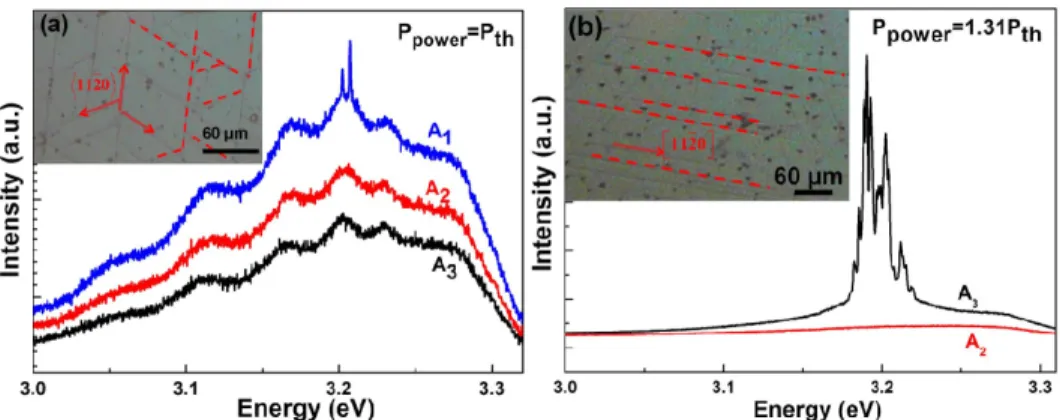
1010 surfaces of wurtzite ZnO have the lowest surface energy by simple bonding density calculation [15]. The development of the cracks is due to the tensile stress induced by lattice mismatch and post-growth cooling. The density of the cracks increases with increasing layer thickness from 3.48 10 cm× 2 −1 for the 555-nm film to 1.29 10 cm× 3 −1 for the 1,200 nm thickfilm. It is also noted that most cracks form networks with 3-fold symmetry in the thick film, shown in Fig. 3(a), but are mostly parallel lines in the thin film, shown in Fig. 3(b). The crack networks with higher density in the thick film provide the closed-loop paths for RL and reduce the RL threshold. On the other hand, the parallel fractures with lower density in the thin film are not sufficient to provide closed-path loops required for RL.
Fig. 3. Emission spectra of the (a) 1,200 and (b) 555 nm thick ZnO films taken under fixed pump power and variable excitation area. The blue, red, and black curves, were taken with pumping area of 1.13 × 10⁻⁴ (A
1), 7.85 × 10⁻⁵ (A2), and 5.03 × 10⁻⁵ cm2 (A3), respectively. The insets illustrate the optical microscope images of the sample surface.
To verify that the high density of crack networks facilitate the RL action via strong multiple light scattering but not the low density parallel ones, we measured the emission spectra of the two samples with fixed pumping power but varying the pumping area. The spectra taken with decreasing illuminated area, (A1) 1.13 × 10⁻⁴, (A2) 7.85 × 10⁻⁵ and (A3) 5.03 × 10⁻⁵ cm2 are depicted by the blue, red, and black curves, respectively, in Figs. 3(a) and 3(b). For the thick film in Fig. 3(a), the spectra collected from the two small excitation areas show smooth intensity variation. When the excitation area increases up to 1.13 × 10⁻⁴ cm2, discrete sharp lasing peaks emerge as the lights are scattered by sufficient boundaries defined by the crack networks and closed-loops are formed. According to the RL theory, the lasing threshold is proportional to the critical pumping area to the power of −2/3 or A-2/3 [7]. If a closed-loop path was too short, the amplification along the loop would not be high enough to achieve lasing. Since the larger excitation area covers the more closed-loop paths for light, RL action could occur in more cavities formed by recurrent scattering. In other words, when an excitation area exceeds the threshold area, closed-loop paths can be formed through multiple scattering in the excitation area and the RL action can be achieved. Based on the RL theory, the stimulated emission peaks appear as the pump diameter exceeds 100 μm (corresponding to 1.13 × 10⁻⁴ cm2), which is close to the calculated cavity length of 92 μm derived from the measured FSR of the lasing modes. This result supports the speculation that high density crack networks formed in the thick ZnO layer facilitate multiple scattering and the RL emerges as the critical pumping area is reached. The intense emission peaks randomly distributed in location on top of the plateau of spontaneous emission in Fig. 2(a) are the RL modes caused by stimulated photons being strongly scattered in gain media, in which closed-loop paths can be formed through multiple scattering by the crack networks.
In order to understand the lasing characteristics of the thin sample (555 nm), we fixed the pumping power at 65 mW and varied the excitation area to observe the change in emission spectrum. As shown in Fig. 3(b), the lasing modes emerge as the pumping area decreases,
with more than one set of equal-spacing peaks under a gain profile of ZnO due to different cavity path lengths [17]. So the observations of excitation area dependence and Gaussian emission pattern shown in Fig. 2(b) suggest that the stimulated emission of the thin film should result from resonant oscillation in a vertical cavity formed by the two end-surfaces of the ZnO film, a conventional FP cavity. And, the resonant peaks should not be associated with the longitudinal lasing modes, because the calculated cavity length of 52 μm is too long to match the film thickness. They may be from the high-order transverse Hermite-Gaussian modes if curved surface exists on the air-ZnO interface.
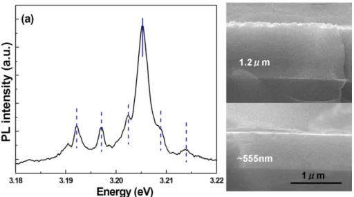
The expanded lasing spectrum of the thin sample is shown in Fig. 4(a). By using the film thickness 555 nm as the cavity length and the refractive index of ZnO at UV range (n ≈2.45), we determine that the significant lasing peak at 3.205 eV corresponds to the 7th longitudinal mode from the FP cavity model. The resonant frequency of the transverse Hermite-Gaussian modes can be expressed by [18]
1 2 1 , , 1 cos 1 2 h k q c h k L v q nL π − R + + = + − , where q is the longitudinal mode number, h and k are the transverse mode numbers, and L is
the cavity length corresponding to the film thickness. Note that R is the average radius of curvature of reflection surface (mirror), which could be formed by a curved film surface due to columnar growth nature of ZnO along the c-axis [19]. From the transverse mode spacing of around 4.8 meV marked by the dashed lines in Fig. 4(a), we estimated the radius of curvature R to be ~510 μm. The obtained radius of curvature is much larger than the layer thickness; this implies the corresponding surface is very smooth.
Figure 4(b) illustrates the cross-sectional SEM images of the two samples. The surface of the thick film (upper panel) is too rough to retain the high reflection efficiency and fails to serve as a good reflector required for a FP cavity. Moreover, the high density of crack networks formed in the thick film enhances multiple scattering and favors the RL action. Under this circumstance, RL action dominates the emission spectrum of the thick film. In contrast, the high crystalline quality and smooth interfaces of the thin sample, together with the good thermal conductivity of Si wafer, which effectively reduces the thermal induced optical deterioration, yield high reflectance of above 50% in the lasing range and lead to low-threshold FP lasing action. In addition, the lower crack density effectively raises the lasing threshold of RL action. The lasing action of the thin film is thus ascribed to the transverse Gaussian modes sustained by the vertical FP cavity. These results are consistent with the report by Kalusniak et al. [12], which demonstrated that pure RL typically requires a larger gain than standard FP feedback. In our case, we observed RL only from the thick film as a result of high crack networks enhanced multiple scattering and large surface roughness that is unfavorable for FP. The low crack density and flat surface of the thin sample facilitate FP lasing action and are unfavorable to multiple scattering; therefore only FP lasing was observed.
For the samples of much smaller ZnO thickness, such as 25, 81, 176, and 345 nm, they are crack-free. Their emission spectra only exhibit emission bands attributed to the exciton-exciton scattering and electron-hole plasma under increasing pumping. Neither RL nor FP lasing was observed. The reasons for not observing random lasing or Fabry-Perot type lasing in other samples of much smaller thickness may be partly because no cracks were formed under the critical thickness that is required for random lasing or not enough gain in much smaller thickness films that require even larger lasing thresholds; and partly because the larger free spectral range with much smaller thickness so that the cavity resonance may not match with the gain profile of the material.
Fig. 4. (a) Emission spectrum from the thin film above the lasing threshold. The solid and dashed lines mark the center of the lasing modes from the vertical cavity model and transverse Hermite-Gaussian modes, respectively. (b) Cross-sectional SEM images of the ZnO epi-layers, the ZnO layer thickness of the upper and lower images are 1,200 and 555 nm, respectively.
4. Conclusion
Lasing modes of different origins, vertical FP cavity and RL, were observed in ZnO epi-films of different thickness grown on Si(111) substrates. The thickness dependent structural features, including surface roughness and crack density and arrangement, play the key roles in active modes selection. High density of crack networks found in the thick film (~1,200 nm) provide sufficient network scattering boundaries, form closed-loops required for random lasing action and give rise to the spatially scattered emission peaks. The lasing action of the thin film (~555 nm) with low crack density and smooth surface is originated from the FP cavities formed by the ZnO-air and ZnO-substrate interfaces. The emission spectrum of the thin sample shows a Gaussian-like profile, characteristic of the transverse Gaussian modes.
Acknowledgments
This work is supported by the Natural Science Council of Taiwan under grant NSC-99-2112-M-006-017-MY3 and NSC100-2112-M-213-002-MY3.