bias is able to induce phase transformation of Cu6Sn5共⬘-Cu6Sn5↔ -Cu6Sn5兲 without thermal annealing. The nonbias-deposited
films showed electrochemical characteristics of the low-temperature⬘-Cu6Sn5phase, whereas the −150 V bias-deposited films
showed properties of the high-temperature-Cu6Sn5phase.
© 2007 The Electrochemical Society. 关DOI: 10.1149/1.2712830兴 All rights reserved. Manuscript submitted September 22, 2006; revised manuscript received January 11, 2007. Available electronically March 16, 2007.
Recently, lithium-ion batteries, especially for multifunction por-table electronic devices, have been of great interest. Many research-ers have focused on searching for new electrode materials and for further understanding of the redox processes in the electrode mate-rials. Among them, alloy-type anode materials have been widely studied due to their large specific capacities. However, the alloy anodes generally show poor cycling properties, due to their large volume changes during lithiated/delithiated processes; this has lim-ited their practical applications. Recently, the possibility of modify-ing the properties of Sn anodes has motivated investigation of Sn-based alloys and intermetallic compounds, MxSny 共M: inactive
element兲, such as Cu–Sn,1-5Ni–Sn,6-8and Fe–Sn.9,10During charge-discharge cycles, the elemental Li reacts with MxSny compounds
and forms brittle Li–Sn alloys, which are embedded in the M matrix. The relatively ductile, inactive M matrix of such compounds is able to endure large stresses caused by significant expansions and con-tractions of volumes.
Among these anode materials, Cu6Sn5 anode materials show unique electrochemical characteristics. Different crystal phases, i.e.,
⬘
-Cu6Sn5and-Cu6Sn5, exhibit different reactions with lithium. A well-crystallized-Cu6Sn5phase obtained by high-temperature an-nealing 共⬃400°C兲 reacts with lithium by an intercalation/ deintercalation process, whereas the nanocrystalline or amorphous ⬘
-Cu6Sn5phase alloys and dealloys with lithium during cycling.2,5 However, typical weight capacity of Cu6Sn5 is around 200 mAh/g,2,5which is approximately 56% of the theoretical capac-ity. Although it is lower than the capacity of the current graphite anodes共⬃372 mAh/g兲, the specific volumetric capacity of Cu6Sn5 is as high as 1656 mAh/mL, which is two times higher than that of graphite. The high specific volumetric capacity and the intercalation characteristics make the Cu6Sn5 anodes of potential interest in lithium-ion batteries.This study is focused on the exploitation of the unique electro-chemical characteristics of Cu6Sn5 thin films. In this research, Cu6Sn5thin films have been prepared by cosputtering of Cu and Sn targets with in situ substrate bias. The substrate bias modifies the films’ crystal structures and therefore the films’ electrochemical properties. The results show that in situ bias is able to induce phase transformation of Cu6Sn5 共
⬘
-Cu6Sn5↔ -Cu6Sn5兲 without ther-mal annealing.Experimental
The Cu6Sn5thin films were prepared by magnetron cosputtering and deposited on stainless steel substrates using pure Sn and Cu 共99.99%兲 targets 共2 in. in diameter兲. The power sources for Sn and Cu targets were radio frequency共rf兲 and dc power supplies, respec-tively. Figure 1 shows the sputter system. The substrate holder was located between the targets, and the distance between the targets and substrate was 11 cm. The working gas was 99.99% pure argon and the gas flow was 15 sccm during sputtering. The working pressure was maintained at 1.33 Pa for all deposition processes. The power levels applied on the Sn and Cu targets were 25 and 30 W, which resulted in the stoichiometric composition of Cu6Sn5thin films. The currents on the substrate holder were monitored and used as an indicator for the precise control of the deposition process under different substrate bias. Cu6Sn5films were deposited with different levels of negative substrate bias, namely: −20, −40, −60, −80, −100, −120, and −150 V. For the films deposited without substrate bias 共0 V兲, the substrates were simply grounded. The deposition time was controlled to obtain the same film thickness共⬃120 nm兲 for different bias conditions. The atomic ratios of Sn and Cu were measured by an inductively coupled plasma-atomic emission
spec-*Electrochemical Society Active Member.
z
trometer共ICP-AES兲. The films’ crystallography was characterized by X-ray diffraction共XRD兲 using a Rigaku D/MAX2500 X-ray dif-fractometer with Cu K␣ radiation 共wavelength 1.5405 Å兲. The sur-face morphology was observed by a JOEL JSM-6700 field-emission scanning electron microscope共FESEM兲.
The deposited films were packed in coin cells 共size no. 2032兲 with the following configuration: Li foil 兩1 M LiPF6 in ethylene carbonate and ethyl methyl carbonate mixed solution共volume ratio 1:2兲兩 Cu6Sn5. The Li foil was also used as the reference electrode. All cells were assembled in an Ar-filled glove box. The charge-discharge and cycle life tests were performed using an electrochemi-cal work station共Jiehan ECS-5000, Taiwan兲. The cells were charged 共lithiated兲 and discharged 共delithiated兲 at constant current density of 50A/cm2between voltage ranges of 0 and 2 V at a constant tem-perature of 25°C.
Results and Discussion
Different substrate biases were applied to attract ions from the plasma to the substrate. These ions contributed to the current flow through the substrate holder. The currents, measured as a function of different negative substrate bias on the substrate holder, are shown in Fig. 2. The currents共i.e., Ar+ flux兲 increase with the substrate bias, which means that negative bias accelerates positive argon ions 共Ar+兲 toward the substrate. These ions bombard on the growing films with energy equal to the difference between the plasma poten-tials and bias voltages. The increased ion-flux bombardment pro-vides extra energy for grain growth and greatly influences the film crystallography and morphology. However, if a negative bias is too extreme, it may also cause damage to the films.
Figure 3a-e shows the surface morphologies of the deposited films as a function of substrate bias. The nonbiased and low-biased 共0–60 V兲 films exhibit similar morphologies, and only the nonbi-ased sample is shown here共Fig. 3a兲. For the nonbiased sample, the film surface is composed of nanosized primary particles共5–10 nm兲, which aggregate into clusters of 50–80 nm共Fig. 3a兲. The clusters loosely disperse on the film surface, and the spaces between the clusters can be clearly observed. As the bias increases to −80 V 共Fig. 3b兲, the sizes of the clusters shrink slightly and become more uniform. The film surface is denser because the −80 V bias is able to induce ion bombardment with enough energy to result in the rearrangement of adatoms and the formation of a denser and smoother surface. This is known as the atomic peening effect.11,12
As the bias exceeds −100 V共Fig. 3c兲, individual particles with much greater sizes form on the surface, and the morphology is com-pletely different. At −120 V of bias共Fig. 3d兲, the surface particles grow into large structures, and some neckings form between par-ticles. At −150 V 共Fig. 3e兲, the particle size can be as large as
⬃100 nm. This evolution of surface morphology can be attributed to the bias-induced ion bombardment, which provides extra energy input during film growth. The extra energy enhances grain growth, and the physical ion bombardment results in redistribution of the surface adatoms, which fills the space between surface grains.12As a consequence, the film morphology is composed of large grains with unclear boundaries共Fig. 3e兲.
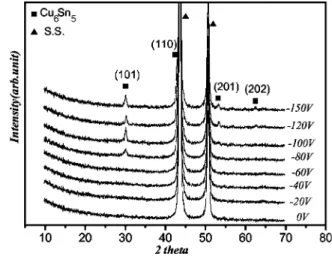
Figure 4 shows the XRD patterns of Cu6Sn5thin films deposited with different substrate biases. The crystallinity changes are corre-lated with the surface morphologies. The nonbiased and low-biased films exhibit low-intensity diffraction peaks, indicating near-amorphous features of the films. As the substrate bias increases to −80 V, the crystallinity of Cu6Sn5thin films is gradually enhanced. Figure 2. Currents measured on the substrate holder at different negative
substrate bias.
Figure 3. Surface morphologies of the films deposited with substrate biases
of共a兲 0, 共b兲 −80, 共c兲 −100, 共d兲 −120, and 共e兲 −150 V.
well-crystallized features共−150 V films兲. Figure 5a-c shows the 1st, 2nd, and 5th charge/discharge curves for Cu6Sn5films deposited at 0, −100, and −150 V bias. At the first charge, the capacity of the 0 V film exceeds the theoretical capacity of
⬘
-Cu6Sn5 共608 mAh/g兲. The extra capacity might be due to the formation of a solid-electrolyte-interphase 共SEI兲 layer, which is produced as the active elemental Sn reacts with the electrolyte at the first charging step. The reversible capacity for the 0 V film achieves 587 mAh/g, which is close to the theoretical capacity of⬘
-Cu6Sn5. The −100 and −150 V films exhibit relatively lower reversible capacity com-pared with that of 0 V films. The higher capacity of 0 V films can be attributed to their nanosized features共Fig. 3a兲, which result in larger surface area and activity. The curves of these films共shown in Fig. 5兲 also exhibit slightly different potential plateaus. More de-tailed information can be obtained from the dQ/dE curves as shown in Fig. 6. Extreme bias共−100 and −150 V in Fig. 6b and c兲 depos-ited films show high intensity redox peaks due to better crystalliza-tion. Figure 6c clearly shows that a reduction peak共marked by a dashed line兲 near 0.4 V has developed for the −150 V bias-deposited film. In addition, the sharp reduction peak near 1.25 V at the first cycle for the 0 V deposited film共Fig. 6a兲 is not recorded in the films deposited at −100 and −150 V共Fig. 6b and c兲, where two distinctive peaks appear around 1.25 V. This suggests that the reac-tions during the first charge-discharge cycle differ between the nano/ amorphous Cu6Sn5and the highly crystallized Cu6Sn5.Recently, Wang et al.2reported the electrochemical properties of - and
⬘
-phase Cu6Sn5anodes. It was shown that⬘
-phase Cu6Sn5 reacted with lithium by alloying Li with Sn. For high-temperature-annealed-Cu6Sn5, it has been suggested that lithium reacts with the Cu6Sn5anodes by an intercalation process.1,2,5The alloying and intercalation mechanisms can be distinguished by the occurrence of the intermediate phase during lithiation. For the alloying process, Li directly alloys with Sn, as shown in Eq. 122Li + Cu6Sn5↔ 5Li4.4Sn + 6Cu 关1兴
For the intercalation process, Li enters the lattice of Cu6Sn5and forms metastable LixCu6Sn5phase共Eq. 2兲. Full lithiation also results in Li4.4Sn共Eq. 3兲
10Li + Cu6Sn5↔ 5Li2CuSn + Cu 关2兴
12Li + 5Li2CuSn↔ 5Li4.4Sn + 5Cu 关3兴
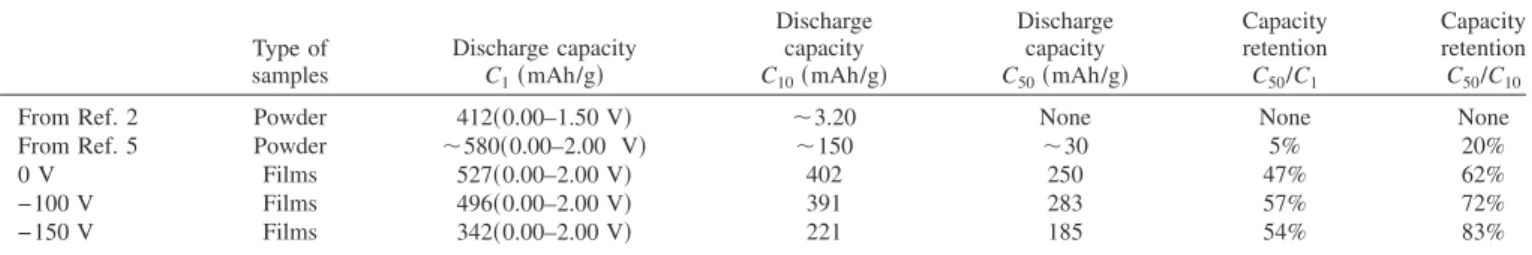
Because the volume change for intercalation is smaller than the change for the alloying process, the cycling stabilities are expected to be different. Figure 7 and Table I show the cycling performances for thin-film anodes deposited with different biases. Although the thin-film anodes still cannot make full use of the active materials, the performance levels of Cu6Sn5 thin films are much better than those of the Cu6Sn5powders, as shown in Table I. In the initial ten cycles, the capacity decreases obviously for the 0 V film, but it maintains a reversible capacity in the following cycles. The capacity dramatically declines to 250 mAh/g共2070 mAh/mL兲 after the 40th
cycle. The capacity fading between the 1st and 50th discharges of the 0 V anode is around 57%共Table I兲. Although the capacity of the −150 V sample also exhibits rapid fading in the initial cycles, it shows much better long term cycling reliability up to the 50th cycle. There is still a capacity of 200 mAh/g 共1656 mAh/mL兲 after 50 cycles, corresponding to a capacity fading of⬃30% 共Table I兲. There is almost no capacity fading between the 10th and 50th cycles, which may be attributed to the different crystallographies of the samples. The 0 V film is amorphous or nanocrystalline; it un-dergoes an alloying process during charge/discharge cycles. The Figure 5. Charge-discharge curves of the films deposited with substrate
−150 V film has a highly crystallized Cu6Sn5 phase, which may favor the intercalation/deintercalation process. As a consequence, the −150 V sample shows better cycling stability with a lower ca-pacity. Because the film crystallography evolves gradually with in-creased substrate bias, it is therefore reasonable to expect that some suitable bias between −150 and 0 V may result in a film with two coexisting phases, where part of the film may favor the alloying process and the other part intercalation. Indeed, as shown in Fig. 7, the −100 V film exhibits an initial capacity between the capacity of the 0 V sample and the capacity of −150 V sample and shows a better cycling stability than the 0 V film. Despite having a slightly lower initial discharge capacity than the 0 V film, the −100 V film exhibits higher reversible capacity and the volumetric capacity is as
high as 2200 mAh/mL at the 50th cycle. The 0 and −100 V films show a trend of continuous decrease in capacity after 50 cycles. The −150 V shows much better cycling stability after 10 cycles, which may eventually compensate for its low capacity as the cycle number increases.
In order to verify the points mentioned above, crystallographic structures of the postcycled films were measured. Figure 8a and b shows the XRD patterns of the postcycled films measured at differ-ent cutoff voltages. Because many of the diffraction peaks from different LixSn alloys directly overlap or have very similar diffrac-tion angles, the possible phases are indexed for each diffracdiffrac-tion peak in Fig. 8a and b. At a cutoff voltage of 0 V, all the films are lithiated to LixSn 共Fig. 8a兲. Almost all the diffraction peaks correspond to
highly lithiated Li3.5Sn and Li4.4Sn phases, except some low-intensity peaks which may belong to Li2.5Sn and Li2.6Sn. Despite the fact that the as-deposited 0 V bias film is amorphous as shown in the XRD data共Fig. 4兲, it exhibits crystalline phases of lithium alloys 共LixSn兲 when charged to 0.4 and 0 V. This phenomenon was also
observed in other Sn-related alloys13,14and pure Sn anodes15with amorphous features. Because the amorphous Sn-alloy thin films are actually composed of nanosized clusters with very high surface en-ergy, the insertion of lithium into the films provides a driving force and readily results in crystallization of LixSn grains. As a
conse-quence, in their charged states, the films exhibit crystalline LixSn
phases.
At the cutoff voltage of 0.4 V, the 0 V film also exhibits diffrac-tion peaks of LixSn alloys as identified in Fig. 8b, indicating the
nature of
⬘
-phase Cu6Sn5. Li2CuSn phase and the unreacted Cu6Sn5 were obtained for −150 V films at the cutoff voltage of 0.4 V and no LixSn phase was found. The results suggest that the −150 V film reacts with Li through an intercalation mechanism and exhibits the nature of the-phase Cu6Sn5. The remaining Cu6Sn5 signals in the XRD spectrum indicate that the grains near the bottom of the film do not react with lithium, which could be due to the large particle size and limited kinetics for lithium insertion. This lack of reaction is also responsible for the low discharge capacity of the −150 V films. As for the −100 V films, diffraction peaks for LixSnand for Li2CuSn can be found, indicating that two phases coexist. For the 0 V films, all the peaks correspond to LixSn phases. The
expected lattice distortion due to intercalation is beyond the resolu-tion of the XRD measurements used here. The results in Fig. 6-8 correlate with each other and suggest that the mechanisms of lithia-tion change with increased bias, and a phase transformalithia-tion of
⬘
-Cu6Sn5↔ -Cu6Sn5may be induced by in situ bias during film deposition.Figure 6. dQ/dE curves of the films deposited with substrate biases of共a兲 0,
共b兲 −100, and 共c兲 −150 V.
Figure 7. Discharge capacity as a function of cycle number for the films
It has been shown that Cu6Sn5films prepared by cosputtering of
Sn and Cu exhibit improved cycling stability. During in situ bias also changes from alloying to intercalation. This change of working mechanism correlates to the performance of electrochemical proper-ties. The 0 V film is an alloy-type anode, showing higher capacity but larger capacity fading during cycling. The −150 V sample is found to react with lithium by an intercalation mechanism, which displays lower capacity but better cycling stability. Suitable bias 共i.e., −100 V兲 results in a film which has both alloying and interca-lation properties and which can achieve higher reversible capacity and cycling stability.
Feng Chia University assisted in meeting the publication costs of this article.
References
1. K. D. Kepler, J. T. Vaughey, and M. M. Thackeray, Electrochem. Solid-State Lett.,
2, 307共1999兲.
2. G. X. Wang, L. Sun, D. H. Bradhurt, S. X. Dou, and H. K. Liu, J. Alloys Compd.,
299, L12共2000兲.
3. Y. Xia, T. Sakai, T. Fujieda, M. Wada, and H. Yoshinaga, J. Electrochem. Soc.,
148, 471共2001兲.
4. S. D. Beattie and J. R. Dahn, J. Electrochem. Soc., 150, 894共2003兲.
5. D. Larcher, L. Y. Beaulieu, D. D. MacNeil, and J. R. Dahn, J. Electrochem. Soc.,
147, 1658共2000兲.
6. G. M. Ehrlich, C. Durand, X. Chen, T. A. Hugener, F. Spiess, and S. L. Suib, J. Electrochem. Soc., 147, 886共2000兲.
7. H. Mukaido, T. Sumi, T. Yokoshima, T. Momma, and T. Osaka, Electrochem. Solid-State Lett., 6, 218共2003兲.
8. Y. L. Kim, H. Y. Lee, S. W. Jang, S. J. Lee, H. K. Baik, Y. S. Yoon, Y. S. Park, and S. M. Lee, Solid State Ionics, 160, 235共2003兲.
9. O. Mao, R. L. Turner, I. A. Courtney, B. D. Fredericksen, M. I. Buckett, L. J. Krause, and J. R. Dahn, Electrochem. Solid-State Lett., 2, 3共1999兲.
10. O. Mao and J. R. Dahn, J. Electrochem. Soc., 146, 414共1999兲.
11. K.-F. Chiu, H. C. Lin, K. M. Lin, T. Y. Lin, and D. T. Shieh, J. Electrochem. Soc.,
153, A920共2006兲.
12. K.-H. Muller, Phys. Rev. B, 35, 7906共1987兲.
13. N. Tamura, M. Fujimoto, M. Kamino, and S. Fujitani, Electrochim. Acta, 49, 1949 共2004兲.
14. N. Tamura, Y. Kato, A. Mikami, M. Kamino, S. Matsuta, and S. Fujitani, J. Elec-trochem. Soc., 153, A1626共2006兲.
15. K.-F. Chiu, H. C. Lin, K. M. Lin, T. Y. Lin, and D. T. Shieh, J. Electrochem. Soc.,
153, A1038共2006兲.
Figure 8. Postcycled XRD patterns of the films deposited with substrate
biases of 0, −100, and −150 V and charged共lithiated兲 to the cutoff voltages of共a兲 0 and 共b兲 0.4 V. The peaks from stainless steel substrates are indicated as SS.