Optical properties and photoconductivity of amorphous silicon
carbon nitride thin film and its application for UV detection
C.W. Chen
a,*, C.C. Huang
a, Y.Y. Lin
a, L.C. Chen
b, K.H. Chen
c, W.F. Su
a aDepartment of Materials Science and Engineering, National Taiwan University, 1, Roosevelt Road, Sec. 4, Taipei 106, Taiwan
b
Center for Condensed Matter Sciences, National Taiwan University, Taipei, Taiwan
c
Institute of Atomic and Molecular Sciences, Academic Sinica, Taipei, Taiwan Available online 28 January 2005
Abstract
Optical properties of amorphous silicon carbon nitride thin films as a function of carbon content have been studied by the spectral micro-reflectometry. The compositions of a-SiCN thin films deposited with different CH4 flow rates were analyzed by X-ray photoemission
spectroscopy (XPS). It was found that the transmittance of a-SiCN thin films decreases with the increasing carbon content; the index of refraction n varies from ~2.0 to ~2.2 and the optical gap (Tauc gap) Eoptvalue progressively decreases from 4.1 to 3.3 eV while the carbon
content changes from 0 to 25% in the films. In addition, a MSM (metal-semiconductor-metal) photodetector device based on the a-SiCN thin film demonstrates excellent selective sensing features with a large photo-to-dark current ratio about 1800 under illumination of the 250 nm UV light source, providing potential applications for low-cost UV detection.
D 2004 Elsevier B.V. All rights reserved.
Keywords: Amorphous silicon carbon nitride; Optical band gap; MSM; UV detector
1. Introduction
Silicon carbide (Si-C) and silicon nitride (Si-N) have wide applications in mechanical, optical and electronic
devices [1]. Carbon nitride, a highly promising hard
material, has also received increasing attention recently
[2]. More recently, a new class of ternary silicon carbon
nitride (SiCN) materials with large (several tens of microns) and well-facet crystals have been grown successfully by microwave plasma-enhanced chemical vapor deposition
(MW-CVD) by Chen et al.[3,4] and Badzian and Badzian
[5]. These newly discovered SiCN crystals have been found
to demonstrate a great potential for applications in semi-conductor technology as well as a structural material. They show excellent mechanical properties with hardness and bulk modulus around 30 and 322 GPa, respectively. The optical investigation of polycrystalline SiCN films shows a
direct band gap of about 3.8 eV and a strong optical
emission around 2.8 eV [4]. The ternary SiCN compound
constitutes an important wide band gap material with a gap energy within the blue-UV spectral region. It is believed that the chemical bonding and atomic local order can be quite complex in the ternary SiCN system. The atomic structure of SiCN crystals can be described as the pseudo a-Si3N4 phase, which shows some deviation from the pure a-Si3N4 pattern in the X-ray diffraction experiment. The similarity of
local atomic structures between SiCN and a-Si3N4 is also
evident from the experiment by the X-ray-absorption
spectroscopy [6]. Composition and bonding analyses
strongly suggest the structure of SiCN to be a solid solution and SiNx and CNx, in that C atoms substitute only for the Si
sites and vice versa [7]. It is expected that carbon content
plays an important role in determining physical properties of a-SiCN thin films. Indeed, it has been reported that the thermal diffusivity, density and hardness of a-SiCN thin
films decreased with increasing carbon content [8]. In this
article, we would like to present a systematical study on the optical and photoconductive properties of a-SiCN thin films
0925-9635/$ - see front matterD 2004 Elsevier B.V. All rights reserved. doi:10.1016/j.diamond.2004.11.027
* Corresponding author. Tel.: +886 2 3366 5202; fax: +886 2 2363 4562. E-mail address: [email protected] (C.W. Chen).
Diamond & Related Materials 14 (2005) 1010 – 1013
as a function of carbon content and the potential applica-tions for UV light detection.
2. Experiment method
Microwave plasma enhanced chemical vapor deposition (MW-CVD, AsTex, 5 kW) systems were employed to grow the SiCN films on the Si(100) and fused silica substrates, respectively. Details of the MW-CVD systems have been
described elsewhere[7]. In brief, a 1.5 kW microwave source
was employed to generate plasma as a mixture of
semi-conductor grade SiH4, NH3,CH4 and H2 gases in various
proportions was used to deposit a-SiCN thin films. By adjusting the flow rate ratio of different gases, films with various compositions were obtained. A microwave power of 1000 W was set and the chamber pressure was kept at about 3.73 kPa during deposition. In order to systematically investigate the bonding configurations of a-SiCN films, we
varied the CH4flow rate from 0 to 30 sccm and kept the flow
rates of SiH4 3 sccm, NH3 30 sccm and H2 100 sccm
unchanged during deposition. Incorporation of hydrogen in the film is inevitable in most CVD process. It has been reported that the a-SiCN films with and without hydrogen incorporation prepared by CVD and IBSD (ion-beam sputtering deposition), respectively, exhibit similar
compo-sitions and bonding states of C, N, and Si[9]. Incorporation of
hydrogen assists the formation of C–H, N–H and Si–H bonds in the films, resulting in the termination of dangling bonds of the a-SiCN network. The chemical composition and bonding states of the a-SiCN films were determined by a Perkin-Elmer
Phi 1600 XPS system with a (800-Am)2sampling area and
11.75 eV pass energy. MgKaradiation of 1253.6 eV was used
as the X-ray source, with a line width of 0.7 eV. The optical properties of refractive index (n and k) and transmittance and film thickness were determined by the spectral micro-reflectometry (Mission peaks optics, MP100-M), by measur-ing the interference between incident and reflected light with wavelengths ranging from UV to visible range (250–1000 nm). All the samples for optical properties measurements were deposited on the quartz substrates. From the phase shift, the film thickness and refractive index (n and k) can be determined. The photovoltaic device with a MSM structure was fabricated by depositing the 800 nm thick a-SiCN film on the silicon substrate and evaporating the Au on top to form the electrode. Photocurrent measurements were completed using a 300 W Xenon lamp (Oriel) coupled to a monochromator as an illumination source and a Keithley 6487 source measure-ment unit to obtain the current and voltage.
3. Result and discussion
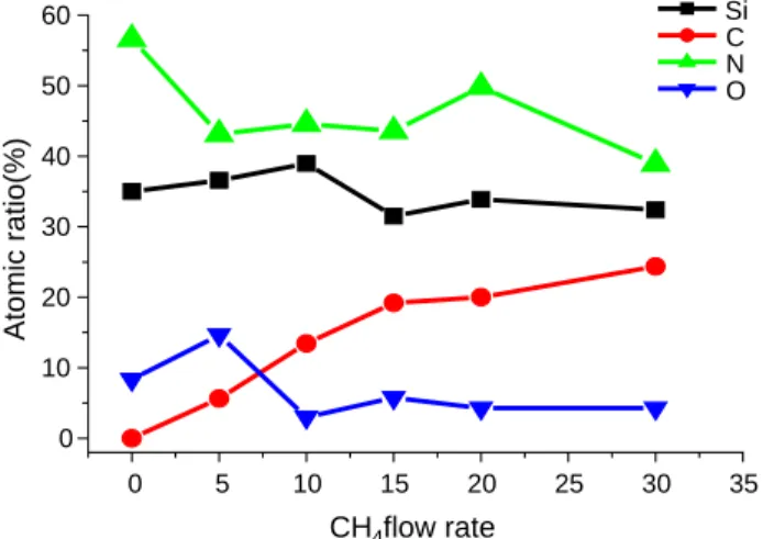
The composition of a-SiCN thin films deposited with
different CH4flow rates determined by XPS measurement is
shown inFig. 1. It is shown that the C content in the SiCN
films gradually increases with the increasing CH4flow rate
up to 15 sccm and reaches to a value around 25% for the 30
sccm CH4 flow rate. No significant variation of carbon
content has been found in the a-SiCN thin films with further
increasing the CH4 flow rate under current experimental
conditions. Oxygen as impurity was found in all the deposited samples and the percentage of the oxygen content was kept below 5% for the films deposited with the CH4
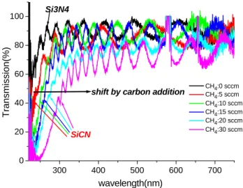
flow rates higher than 10 sccm. Fig. 2 shows the
trans-mission spectra of a-SiCN thin films with various carbon content. The film thicknesses for these films are 900(0 sccm), 950(5 sccm), 1040(10 sccm), 1060(15 sccm), 1095(20 sccm), 1020(30 sccm) nm, respectively. The average transmittance for these films in the visible light range is between 70%-90%. In addition, the optical absorption band edge shifts toward the lower energy position as the carbon content increases. The dispersion of refractive index for a-SiCN thin films with various carbon
content is shown inFig. 3. The refractive index values n(k)
of the a-SiCN thin films increase as the carbon content increases. The refractive index of the a-SiCN thin films varies from ~2.0 to ~2.2 while the carbon content changes from 0 to 25%. These values are relatively closer to that of
Si3N4 (~2.0) compared to that of SiC (~2.6) due to the
similarities of local bonding configurations between SiCN
and Si3N4 as mentioned above. The absorption coefficient
a(k) were deduced from the extinction coefficient k(k) measured by the spectral reflectometry and, subsequently, the optical band gap of the a-SiCN thin film Eopt, is obtained
from the Tauc plot[10], (ahv)1/2=BTauc(hv-Eopt) where BTauc
is a constant factor and hv is the photon energy. Fig. 4
shows the variation of the optical band gap (Eopt)obtained as a function of carbon content. It is clearly observed that the
Eopt values progressively decrease with increasing carbon
content in the films. This result is consistent with the
theoretical calculations [11], which indicates that the
addition of C atoms in the a-Si3N4network will lower the
value of conduction band minimum (CBM) due to the high
0 5 10 15 20 25 30 35 0 10 20 30 40 50 60 Atomic ratio(%) CH4flow rate Si C N O
Fig. 1. The composition of a-SiCN thin films deposited with different CH4
flow rates determined by XPS measurement.
localization of C compared to Si. From the above results, it is shown that optical properties of a-SiCN thin films can be tuned by varying the carbon content, providing the ability of band gap engineering.
Fig. 5(a) shows the characteristics of photocurrent-voltage response of the Au/a-SiCN/Si MSM photodetector device under the irradiation of light sources with various wavelengths. The composition of the a-SiCN thin film in the device is Si(35%):C(24%):N(39%):O(2%) with a thickness of 800 nm. It is clearly shown that the photoconductive current of the Au/a-SiCN/Si device increases dramatically for the illuminating light with a wavelength shorter than 350 nm, indicating that the device possesses a selective sensing
feature of good solar-blind ability. The photocurrent Ip to
dark current Idratio (PDCR) defined asIpIdreaches a value of
1800 for the incident light with a wavelength of 250 nm under an applied voltage of 5 V, which is the highest value
so far reported for amorphous SiCN-based materials [12].
The small leakage current for the incident light with a wavelength longer than 350 nm is mainly due to the midgap states of the SiCN thin film in amorphous phase. For
300 400 500 600 700 800 900 2.00 2.05 2.10 2.15 2.20 2.25 Refractive index wavelength(nm) CH4:0 sccm CH4:5 sccm CH4:10 sccm CH4:15 sccm CH4:20 sccm CH4:30 sccm
Fig. 3. The dispersion of refractive index of a-SiCN thin films with various carbon content. 0 5 10 15 20 25 3.2 3.3 3.4 3.5 3.6 3.7 3.8 3.9 4.0 4.1 Optical bandgap(eV) Carbon composition(%)
Fig. 4. Variations of the optical band gap Eopt( Tauc gap) of a-SiCN thin
films with various carbon content.
(a)
(b)
0 1 2 3 4 5 -5.0x10⁻⁶ 0.0 5.0x10⁻⁶ 1.0x10⁻⁵ 1.5x10⁻⁵ 2.0x10⁻⁵ 2.5x10⁻⁵ Current(A) Voltage(V) 250 nm 350 nm 400 nm 500 nm 600 nm 700 nm Dark 0 1 2 3 4 5 -1.0x10⁻⁸ -5.0x10⁻⁹ 0.0 5.0x10⁻⁹ 1.0x10⁻⁸ Current(A) Voltage(V) 250nm 400nm 532nm 600nm 700nm dark Current(A)Fig. 5. (a) Characteristics of photocurrent-voltage response of the Au/a-SiCN/Si MSM photodetector device under the irradiation of light sources with various wavelengths. The composition of the a-SiCN thin film in the device is Si(35%): C(24%): N(39%): O(2%) with a thickness of 800 nm. The photocurrent Ipto dark current Idratio (PDCR) is 1800 for the incident
light with a wavelength of 250 nm under an applied voltage of 5 V. (b) the I-V characteristics of the Au/a-Si3N4/Si device.
300 400 500 600 700 0 20 40 60 80 100
shift by carbon addition
SiCN Si3N4 Transmission(%) wavelength(nm) CH4:0 sccm CH4:5 sccm CH4:10 sccm CH4:15 sccm CH4:20 sccm CH4:30 sccm
Fig. 2. The transmission spectra of a-SiCN thin films with various carbon content. The film thicknesses for these films are 900(0 sccm), 950(5 sccm), 1040(10 sccm), 1060(15 sccm), 1095(20 sccm), and 1020(30 sccm) nm, respectively.
C.W. Chen et al. / Diamond & Related Materials 14 (2005) 1010–1013 1012
comparison, the I-V characteristics of the Au/a-Si3N4/Si
device as shown inFig.5(b) are measured under the same
conditions as mentioned above. In contrast, there is no enhancement of current for the incident light with wave-length from 250 to 700 nm, indicating the highly insulating properties of a-Si3N4. The carbon content therefore plays an important role in determining the photoconductive response of the a-SiCN thin film. The reason for high photosensitivity of the a-SiCN thin film in the UV region is intriguing. It is believed that the significant enlargement of photoconduc-tivity in the a-SiCN thin films may mainly result from the increase of absorption of light and from the enhancement of the conduction of photo-generated carriers as the carbon
content increases. The increasing population of sp2-bonded
CjN or CjC sites with increasing carbon content may also contribute to the increase of photoconductivity due to the delocalization of k orbital characters. The detailed investigation of the transport mechanism depending on the
carbon content in the a-SiCN thin film is on the way[13].
Combined with the excellent thermal stability and with the ability for band gap engineering by varying the carbon content, the a-SiCN based MSM device exhibiting high sensitivity to UV illumination can be further developed into the potential applications of UV photodetectors.
4. Conclusion
Optical properties of the a-SiCN thin films have been investigated as a function of carbon content. It was found that the refractive index n increases as the carbon content increases. On the other hand, the transmittances and the optical band gaps of a-SiCN thin films progressively decrease with the increasing carbon content, providing the ability for band gap engineering. In addition, the simple Au/
a-SiCN/Si MSM device demonstrates excellent selective UV sensing feature, which can be further developed into the potential applications of UV photodetectors.
Acknowledgement
This work is supported by National Science Council, Taiwan (Project No. NSC93-2120-M-002-010) and the US Airforce project (Project No. AFOSR-AOARD-04-4023).
References
[1] M. Dayan, J. Vac. Sci. Technol., A, Vac. Surf. Films 3 (1985) 361; E.C. Paloura, J. Lagowski, H.C. Gatos, J. Appl. Phys. 69 (1991) 3995. [2] M.L. Cohen, Phys. Rev., B 32 (1985) 7988;
A.Y. Liu, M.L. Cohen, Science 245 (1989) 841.
[3] L.C. Chen, C.Y. Yang, D.M. Bhusari, K.H. Chen, M.C. Lin, J.C. Lin, T.J. Chung, Diamond Relat. Mater. 5 (1996) 51.
[4] L.C. Chen, C.K. Chen, S.L. Wei, D.M. Bhusari, K.H. Chen, Y.F. Chen, Y.C. Jong, Y.S. Hunag, Appl. Phys. Lett. 72 (1998) 2463. [5] A. Badzian, T. Badzian, Diamond Relat. Mater. 7 (1998) 1519. [6] Y.K. Chang, H.H. Hsieh, W.F. Pong, M.H. Tsai, K.H. Lee, T.E. Dann,
F.Z. Chien, P.K. Tseng, K.L. Tsang, W.K. Su, L.C. Chen, S.L. Wei, K.H. Chen, D.M. Bhusari, Y.F. Chen, Phys. Rev. 58 (1998) 9018. [7] L.C. Chen, K.H. Chen, J.J. Wu, D.M. Bhusari, M.C. Lin, in: H.S.
Nalwa (Ed.), Chapter 2 in Handbook of Si-Based Materials and Devices, Academic Press, 2001, p. 74, invited book chapter. [8] S. Chattopadhyay, L.C. Chen, C.T. Wu, K.H. Chen, J.S. Wu, Y.F.
Chen, G. Lehmann, P. Hess, Appl. Phys. Lett. 79 (2001) 332. [9] H.C. Lo, J.J. Wu, C.Y. Wen, T.S. Wong, S.T. Lin, K.H. Chen, L.C.
Chen, Diamond Relat. Mater. 10 (2001) 1916.
[10] J. Tauc, R. Grigorovici, A. Vancu, Phys. Status Solidi 15 (1996) 627. [11] C.W. Chen, M.H. Lee, L.C. Chen, K.H. Chen, Diamond Relat. Mater.
13 (2004) 1158.
[12] W.R. Chang, Y.K. Fang, S.F. Ting, Y.S. Tsair, C.N. Chang, C.Y. Lin, S.F. Chen, IEEE Electron Device Lett. 24 (2003) 565.
[13] C.W. Chen, unpublished work.