ARCHITECTURE DESIGN FOR DEBLOCKING FILTER IN H.264/JVT/AVC
Yu-Wen Huang*, To-Wei Chen, Bing-Yu Hsieh, Tu-Chih Wang, Te-Ha0 Chang, and Liang-Gee Chen
DSP/IC Design Lab., Graduate Institute
of Electronics Engineering and
'Department
of
Electrical Engineering, National Taiwan University
.{yuwen, tchen, bingyu, e.ric, thchang, Igchen} @video.ee.ntu.edu.tw
. .
ABSTRACT
This paper,presents an efficient VLSI architecture for the dehlock- ing filter in H.ZWIVT/AVC. We use an array of 8x4 &bit shift registers with reconligurable data path to support both horizon- tal filtering and vertical filtering on the same circuit (a parallel-in parallel-out reconfigurable FIR filter). Two SRAM modules are carefully organized not only for the storage of current macroblock data and adjacent block data but also for the efficient access of pix- els in different blocks. Simulation results show that under 0.25 p m technology. the synthesized logic gate count is only 19.1 K (not in- cluding a 96x32 SRAM and a 64x32 SRAM) when the maximum frequency is 1M) MHz. Our architecture design can easily sup- port real-time deblocking of 720p (1280x720) 30Hz video. It is valuable for platfom-based design of H.264 codec.
1. INTRODUCTION
Experts from ISO/IEC MPEG-4 Advanced Video Coding (AVC) and ITU-T H.264 cooperate together
as
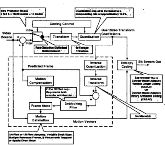
the Joint Video Team (JVT) to develop the emerging standard [I]. The new standard signifi- -candy outperforms previous ones in hit-rate reduction. The func- tional blocksof
H.264, as well as their features, are shown in Fig. 1. Unlike the overlapped motion compensation (OBMC) [2] in H.263 [31 and MPEG-4 141. H.264 adopts the deblocking filter to eliminate blocking artifacts and to achieve much better subjective views. Since the dehlocking filter is located in the DPCM loop, it is required at both the encoder side and the decoder side. The de- blocking filter is much more complex than common low-pass FIR filters that introduce blurring effects on real edges. The conceptof deblocking is to first decide whether the discontinuity between block boundaries is resulted from quantization, different motion vectors, or real edges. Then, different types of filters are selected according to the decision in order to maintain the sharpness of real edges and to smooth the unpleasant block boundaries simultane- ously. The number of taps, set of filter coefficients, clipping func- tions, and threshold values, are all adaptive with different coding modes.
At the decoder side, deblocking filter contributes to a consider- able amount of computation. At the encoder side, motion estima- tion becomes the processing bottleneck. However, pure software implementation of deblocking filter still requires a large amount
of bus bandwidth for platform-based design. For example, CIF (352x288) 30Hz video needs 36 Mbytedsec, and 720x480 30Hz video needs 124 Mbytedsec. Therefore, we proposed a hardware accelerator for deblocking to decrease the processing cycles and
'The author thanks SiS Education Foundation for financial support.
0-7803-7965-9/03/$I7.00 02003 IEEE
Fig. 1. Functional blocks and features of H.264.
the heavy burden of system bus. The rest of this paper is orga- nized as follows. In Section 2, we will review the algorithm of
deblocking in H.264. In Section 3, we will describe our architec- ture design. Simulation results will be shown in Section 4. Finally, Section 5 gives a conclusion.
2. ALGORITHM
In H.264, the transformation is based on 4x4-blocks, and the small- est block size for motion compensation is also 4x4. Therefore, deblocking process checks the boundaries between 4x4 blocks. Deblocking is done macroblock (MB) by macroblock in raster scan order. In each macroblock, horizontal filtering across vertical edges is first executed, and then vertical filtering across horizon- tal edges is applied. The sequential order of edges is shown in Fig. 2. For each boundary between neighboring 4x4-luma blocks, a boundary strength (Bs) is assigned as shown in Fig. 3. If one of the neighboring blocks is intra-coded, a relatively strong filter- ing (Bs=3) is applied. If the block boundary is also macroblock boundary and one of the blocks is intra-coded, an even stronger filtering procedure is applied (Bs=4). If neither of the blocks are intra-coded and at least one of them contains non-zero transform quantized residues, medium filtering strength (Bs=2) is used. If
none of the previous conditions are satisfied, Bs=l when the ref-
Fig. 2. Sequential order of venical edges and horizontal edges in a macroblock. Each square stands for a 4x4-blofk.
Fig. 3. Flowchart for determining the boundary strength.
m
Fig. 4. Chroma boundary strengths. PI PI P, Po "0 7 , b PI
Fig. 5. Convention for describing samples across a boundary he- tween two 4x4-blocks (in horizontal or vertical direction).
Without deblocking (QP=35) With deblocking (QP=35) 39.1616 d B 32.4859 d B
Fig. 6. Subjective views and PSNR values withoutlwith deblock- ing for the first frame of Foreman.
... ... ...
Fig. 7. Architecture design for the deblocking filter.erence frames of two blocks are different or when the reference frames are the same but any component of the two motion vectors has difference more than one pixel sample. Otherwise filtering is skipped (Bs=O). The chroma boundarfstrengths are the same as corresponding luma boundary strengths, as shown in Fig. 4:In the following description. the set of eight samples across a boundary between two 4x4-blocks (in horizontal or vertical direction) is de- noted as shown in Fig. 5 with the actual boundary lying between
PO and qo. Sets of samples across this edge are only filtered if the following conditions
Bs
#
0IPO
-
qol<
aIPI
-POI
< B
141-
qol< B
are all true. Note that a and
0
are Q P (quantization parameter) dependent thresholds. After Bs is determined, two types of filter- ing are specified. In the default case (O<Bs<4), po and qo are filtered with Q P dependent clipping functions. For luma samples, p l and ql are further conditionally filtered. The number of taps is four. In the other case ( B s d ) , a 3-tap filter, a 4-tap filter, or a 5-tap filter is applied on p z , p l , PO, qo, q1 and qz, which depends on the local activity of the luma or chroma eight samples and QPdependent thresholds. Let us skip the details ofthe coefficients of filters. Interested readers can refer to [I] and
[SI.
Figure 6 shows the effect of the deblocking filter.3. ARCHITECTURE
Figure 7 shows the proposed architecture design for the dehlock- ing filter. The solid arrows denote data path, and the dotted ar- rows denote control signals. Before deblocking a macroblock for platfom-hased design, we have to load the macrohlock data (16
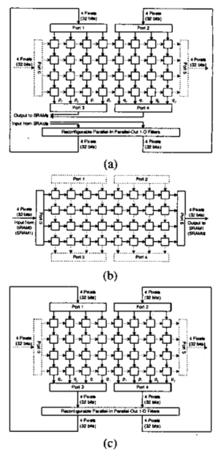
luma 4x4-hlocks. 8 chroma 4x4-blocks) and adjacent block data (8 luma 4x4-blocks. 4 chroma 4x4-blocks) from extemal RAM via system bus to the on-chip SRAM. A parallel-io parallel-out (eight pixels in, eight pixels out) I-D reconfigurahle FIR filter is directly implemented as stated in the previous section. In or- der to support the parallel filter with high utilization, two SRAM modules are carefully organized. As shown in Fig. 8, the hit width of each SRAM is 32 (4 pixels). We classify 4x4-hlocks into different columns ( ~ 0 . ~ 1 0 ) and store 4x1 pixels as one 32-hit word in SRAM. Then, we put adjacent columns of block data in different SRAM modules so that we can access any eight pixels across different columns of blocks. In this way, horizontal filter- ing across vertical edges becomes very easy. However, vertical filtering across horizontal edges are not that straightfonvard. Our solutions will be stated as follows.
Fig.
S.
Organization of on-chip single port SRAM modules.m m
Fig. 9. Processing order of boundaries; (a) horizontal filtering across vertical edges; (h) vertical filtering across horizontal edges.
3.1. Basic Architecture with 2 Single Port SRAM's
In this subsection, we assume each SRAM module has only one readlwrite port. The processing order of block boundaries for both directions is shown in Fig. 9. Our basic idea is to buffer the 8x4 unfilteredlfiltered pixels of two adjacent 4x4-blocks in an 8x4 pixel array with reconfigurable data path in order to support both hori- zontal and vertical filtering on the same I-D filters.
The data path for horizontal filtering is shown in Fig. IO(a). Note that solid arrows denote enabled path while dotted arrows denote disabled path, and each square stands for an 8-hit register. For this architecture, it takes 8 clock cycles to process each pair of
4x4-blocks. In the first 4 cycles. 8x1 pixels are inputted from two SRAM modules into I-D filters. Meanwhile. the filtered pixels are fed to Port1 and Port2 of the pixel array with downward path. In the later 4 cycles, filtered 8x4 pixels are already saved in the array, and we store them hack to the two SRAM's.
The data path for vertical filtering is divided into a loadistore phase and
a
filtering phase, as shown in Fig. IO(h) and (c). re- spectively. First. we assume the filtered 8x4 pixels of previous boundary are already buffered in the array. In the loadlstore phase, the path of pixel array is rightward. It takes 8 cycles to load the 4x8 pixels of a 4x4-block pair belonging to one column, and also to store the 4x8 previously filtered pixels of another 4x4-block pair belonging to the previous column. The load and store can he exe- cuted at the same time without conflict because of the interleaved memory organization. In the filtering phase. the path of pixel array becomes downward. It is clearly that 4 cycles are required to filter the 4x8 pixels and to buffer the filtered results in the array.In sum, if the bit width of system bus is typically 32, we have to spend I60 cycles to load unfiltered pixels from external memory
lo on-chip SRAM's. 8x24=192 cycles to filter in horizontal direc-
tion.(8+l2xl6)+(8+I2~4)x2=312 cycles to filter in vertical direc- tion, and 160 cycles to write filtered pixels from on-chip SRAM's
to external memory. Some,exlra cycles are also required to load the coding information before deblocking. In our implementation,
(a) . .
. . . w , . : w s . . . . . . . .
4-
I=-,
Fig. 10. Data path; (a) horizontal filtering across vertical edges;
(h) vertical filtering across horizontal edges (loadlstore phase): (c) vertical filtering across horizontal edges (filtering phase).
54 cycles are required. The number of total cycles required for deblocking a macrohlock is 878.
3.2. Advanced Architecture with 1 Dual Port SRAM We can pack the pixels, which were originally placed in two sin-
gle
port SRAM'sas
shown in Fig.8,
together into one dual port SRAM as illustrated in Fig. I I , without affecting the data flow. Because a dual port SRAM has two separate readlwrite ports. itcan perform two read operations at the same cycle, as well as two write operations, or one read and one write at the same cycle. It is worthwhile to use one dual port SRAM instead of two single port SRAM's for we can save one power ring on the physical layout.
Fig. 11. Organization of on-chip dual port SRAM.
Table 1. Comparison of architectures synthesized at 100 MHz.
AlChiIeCWI Gate Count CycleslMB Capability
Baric + single pan SRAWs 18.91K 878 1280x72031.6fpr
A d v a n a d c d u a l parlSRAM 18.91K 814 1280x72034.lfpr
Baric + two pon SRAM'r 18.91K 782 1280x720 35.5fpr
Dualarrayr+twoponSFAM'r 20.66K 614 1280x72045.2fpr
cmvll ,"B. a r p s m : 5.nx I- RAM 1,"c. ,E,- 1"0* h l .
IILePr 6 61KIycI. Am) ,.,W. Fig. 12. Advanced processing order of boundaries; (a) horizontal
filtering: (b) vertical filtering; (c) block index.
Fig. 13. Advanced data path for horizontal filtering
Next, we modify the processing order of boundaries as shown in Fig. l2(a)(b) without affecting the data dependency in Fig. 2. The block index is shown in Fig. 12(c). The main idea is stated as follows. For example, for horizontal filtering, after boundary I is processed, we only have to write block 1 from m a y to SRAM. As for block 6. we can directly send it back to the filters with block I I
from SRAM to keep on processing boundary 2. At this moment, in order to support the new processing order, the data path also has to be reconfigured as Fig. 13. In this way, the number of cycles for horizontal filtering is decreased to 152. The data Row and data path of vertical filtering can be easily derived with the help of Fig. 12(b). The number of cycles for vertical filtering is reduced to 288, and the number of total cycles becomes 814.
3.3. Parallel Architecture with 2 Two Port SRAM's
If we replace each of the two single port SRAM's by a two
pon
SRAM (one read port and one write port). for horizontal filtering, we do not need the 8x4 pixel may. We can directly get 8x1 pix- els from two SRAM's, filter 8x1 pixels, and write them back to SRAM's at the same time. However, for vertical filtering. the 8x4 pixel m a y is still necessary because the vertical filtered 8x1 pixels belong to 8 separate words in one SRAM. That is, the data path for vertical filtering is still the same as Fig. IO(b) and (c). There- fore, it only requires 4x24=96 cycles for horizontal filtering, and the number of total cycles is reduced to 782. If we can have 2 two port SRAM's and dual 8x4 pixel m a y s in parallel, the venical filtering can be further accelerated. In this way, the number of cy- cles required for vertical filtering becomes 12x24/2=144, and the number of total cycles becomes 614.
Table 2. Comparison of bus bandwidth.
Specifications Software (RISC) Our An'hitecmre I-=) ,MhYlruur)
CIF (352x240) MHz 36.50 15.21
NTSC (120x480) MI11 124.42 51.84
72Op (1280x720) 30Hz 331.18 138.24
4. SIMULATION RESULTS
We described our architecture by Verilog HDL and synthesized the circuit using 0.25 p m Artisan CMOS cell library by Synopsys De-
sign Analyzer with critical path constraint set to 10 ns (100 MHz). The results are shown in Table 1. The processing capability of our architecture can easily support real-time deblocking of 720p 30Hz video, and the synthesized gate count is very small. Table 2 shows the comparison of system bus bandwidth for platfom-based de- sign. Our architecture can save more than 50% of the bandwidth compared to software implementation of the deblocking filter (pro- cessed by RISC). According to the simulation results, our design is a good candidate of deblocking filter for the platform-based design of H.264 coding systems.
5. CONCLUSION
In this paper. we contributed a hardware deblocking accelerator for H.264llVTlAVC. The major idea is to use interleaved memory or- ganization and an 8x4 pixel m a y with reconfigurable datapath to support one parallel-in parallel-out reconfigurable I-D filter. Sim- ulation results show that the processiiig capability of the proposed architecture is very high (real-time deblocking of 1280x720 30He video operating at 66-94 MHz), and the area is very small (around 19K logic gates
+
96x32 SRAM+
64x32 SRAM). It is very suit- able to be integrated into H.264 coding systems.6. REFERENCES
Comniilree DraJi of Join1 Wdeo Specifcarion (ITU-T Rec.
H.264 and lS0NEC 14496.10 AVC). July, 2002.
M.T. Orchard and G.J Suillivan, "Overlapped block mo- tion compensation: an estimation-theoretic approach," IEEE Trans. Image Processing, pp. 693-699, Sep. 1994.
Video Coding for Low
Bit
Rate Communicarion. ITU-T Rec- ommend H.263, Feb. 1998.Information Technology - Coding of Audio-Visual Objects - Pan 2; Visual, ISONEC 144496-2, 1999.
Join1 Wdeo Team (JWJ sofrwnre JMb.ld, March, 2003.