Metallurgical Reaction of the Sn-3.5Ag Solder and Sn-37Pb
Solder with Ni/Cu Under-Bump Metallization in a Flip-Chip
Package
CHIEN-SHENG HUANG,1JENQ-GONG DUH,1,3and YEN-MING CHEN2
1.—Department of Material Science and Engineering, National Tsing Hua University, Hsinchu, Taiwan 300. 2.—Department of Material Science and Engineering, National Chiao Tung Univer-sity, Hsinchu, Taiwan 300. 3.—E-mail: [email protected]
Several international legislations recently banned the use of Pb because of environmental concerns. The eutectic Sn-Ag solder is one of the promising candidates to replace the conventional Sn-Pb solder primarily because of its excellent mechanical properties. In this study, interfacial reaction of the eutec-tic Sn-Ag and Sn-Pb solders with Ni/Cu under-bump metallization (UBM) was investigated with a joint assembly of solder/Ni/Cu/Ti/Si3N4/Si multilayer structures. After reflows, only one (Ni,Cu)3Sn4intermetallic compound (IMC) with faceted and particlelike grain feature was found between the solder and Ni. The thickness and grain size of the IMC increased with reflow times. Another (Cu,Ni)6Sn5IMC with a rod-type grain formed on (Ni,Cu)3Sn4in the interface between the Sn-Pb solder and the Ni/Cu UBM after more than three reflow times. The thickness of the (Ni,Cu)3Sn4 layer formed in the Sn-Pb system remained almost identical despite the numbers of reflow; however, the amounts of (Cu,Ni)6Sn5 IMC increased with reflow times. Correlations between the IMC morphologies, Cu diffusion behavior, and IMC transforma-tion in these two solder systems will be investigated with respect to the microstructural evolution between the solders and the Ni/Cu UBM. The morphologies and grain-size distributions of the (Ni,Cu)3Sn4 IMC formed in the initial stage of reflow are crucial for the subsequent phase transformation of the other IMC.
Key words: Sn-Ag solder, under-bump metallization, intermetallic compound, phase transformation, diffusion
1509 (Received April 19, 2003; accepted June 17, 2003)
INTRODUCTION
The Sn-Pb solder alloys are widely used in today’s electronic package. However, because of the toxic effect of Pb on human beings and the environment, several Pb-free solder alloys have been investigated to replace the Sn-Pb alloys.1–4 The eutectic Sn-Ag solder alloy with a eutectic point of 221°C is one of the candidates because of its excellent mechanical properties.5
Flip-chip technology (FCT) exhibits several advantages, such as high input/output connects, high-frequency performance, and low cost. It has
thus become one of the most attractive processing methods in microelectronics.6,7 The major function of the under-bump metallization (UBM) is to connect the Si substrate and the solder bump. The Ni-based UBM is of interest in FCT because of the low growth rate of the Ni-Sn compound and limited spalling effect.8,9 The Cu metallization possesses excellent electrical properties and is widely used as interconnects in FCT.10 The effect of Ni thickness and reflow times on the interfacial reactions between the Pb-Sn solder and the Ni/ Cu UBM was recently discussed.11 The phase transformation of intermetallic compounds (IMCs) and related phase-equilibrium behavior was also reported.12
IMCs in these two systems. According to the microstructural evaluation and the mechanism of IMC transformation, the morphology effect on Cu diffusion in the joint assembly could be probed and assessed.
EXPERIMENTAL PROCEDURE
Two different solder alloys were used in this study: the lead-free Sn-3.5Ag solder and the eutectic Sn-37Pb solder. The UBM structure used is shown in Fig. 1. The top metal of the Si wafer was Cu, which acted as an interconnection line. The adhe-sion layer was sputtered Ti of 1,000 Å. For an elec-troplated seed layer, 5,000-Å Cu was then sputtered on Ti. The electroplated Cu with 5-µm thickness was further deposited on the metallized substrate. The 3-µm Ni was electroplated on the top of electro-plated Cu to join with the solder bump. After the UBM was plated on to the Si wafer, the solder bumps were then electroplated. All metal films were deposited consecutively without breaking vacuum.
Solder reflows were conducted in an infrared sol-der-reflow oven. The peak temperatures of the re-flow profile for Sn-Ag and Sn-Pb bumps were 260°C and 225°C, respectively. The cycles of solder reflow were from one to ten times.
The Si dies were cold-mounted in epoxy, sectioned using a slow-speed diamond saw, ground, polished,
program.
RESULTS AND DISCUSSION Interfacial Reaction between the Sn-3.5Ag Solder and the Ni/Cu UBM during Multiple Reflows
Figure 2 shows the cross-sectional images of the interface between the Sn-3.5Ag solder and the Ni/Cu UBM after one, four, and ten reflow times. Only one type of interfacial product was found be-tween the solder and Ni. After detailed composition analysis by EPMA, it appears that the composition of the reaction product is homogeneous in each sample. Related EPMA quantitative-analysis re-sults are listed in Table I. The ratio of (Ni ⫹ Cu) to Sn was very close to 3:4, and the IMC could thus be denoted as (Ni,Cu)3Sn4. The detection of Cu content in the Ni3Sn4IMC indicated that Cu atoms diffused through Ni and then formed the Ni3Sn4 IMC, as discussed in a previous study.11 It should be noted that the compositions of the (Ni,Cu)3Sn4IMC listed in Table I are more or less identical in the samples during reflow. In other words, the amounts of Cu dissolution remained nearly identical as reflow times increased.
After the first cycle of reflow, the scalloped-type (Ni,Cu)3Sn4IMC exhibited a rather round interface. However, with increasing reflow times, the interface between the solder and Ni became wavy, as indi-cated in Fig. 2. For example, the nodule size of the (Ni,Cu)3Sn4 IMC formed after one reflow was less than 1 µm. After ten reflow times, larger size nodules of 2–4 µm in diameter could be found between the solder and Ni. The growth of the (Ni,Cu)3Sn4IMC was evident during reflow.
To investigate the morphologies of these two IMCs more closely, an etching solution was em-ployed to remove the bulk solder. Figure 3 shows the top-view micrographs of the IMC in the Sn-Ag system after one, four, and ten reflow times, respec-tively. The (Ni,Cu)3Sn4IMC exhibited a faceted and particlelike morphology. Similar observation of the Ni3Sn4 IMC was reported in the literature,16,17 yet the grain sizes were different. A combination of the cross-sectional images in Fig. 2 as well as the top-view morphology demonstrated in Fig. 3 showed that the grain sizes of the (Ni,Cu)3Sn4 IMC increased with the numbers of reflow times.
Statistically, the grain-size distribution of the (Ni,Cu)3Sn4 IMC formed after ten cycles of reflow was broader than that formed after one reflow. In fact, the grain sizes of the IMC formed after one, four, and ten reflow times are 0.6–1.5 µm, 1.4–3.5 µm, and 1.5–5.0 µm, respectively. As a result, a wavy interface was revealed between the solder and UBM after ten reflow times.
Interfacial Reaction between the Sn-37Pb Solder and Ni/Cu UBM during Multiple Reflows
The cross-sectional images of the interface be-tween the Sn-37Pb solder and the Ni/Cu UBM after one and ten reflow times are shown in Fig. 4a and b, respectively. After one reflow, only one layered-type (Ni,Cu)3Sn4 with 1-µm thickness formed between the solder and the Ni/Cu UBM. However, another is-landlike (Cu,Ni)6Sn5IMC lying on the layered-type
(Ni,Cu)3Sn4 was detected between the solder and Ni after more than three reflow times. The related phase transformation and phase-equilibrium behav-ior of IMCs have been discussed elsewhere.11,12 To equilibrate with (Cu,Ni)6Sn5, the Cu contents in (Ni,Cu)3Sn4 increased with decreasing distance between (Cu,Ni)6Sn5and (Ni,Cu)3Sn4. The Cu diffu-sion thus plays a key role in the IMC formation in the interface of the Sn-Pb and the Ni/Cu UBM after multiple reflows. On the other hand, the thickness of the (Ni,Cu)3Sn4 IMC was nearly identical even after ten cycles of reflow, as indicated in Fig. 4a and b. Nevertheless, the amounts of the (Cu,Ni)6Sn5 IMC increased with the reflow cycles. That is to say, for the Sn-Pb system, the phase transformation of the (Cu,Ni)6Sn5 IMC occurred, instead of the growth of the (Ni,Cu)3Sn4 IMC after more than three reflow times.
The top-view morphologies of IMCs in the Sn-Pb system during multiple reflows are illustrated in Fig. 5. The morphologies of the (Ni,Cu)3Sn4 IMC formed in the Sn-Pb system after one reflow were faceted and particlelike, similar to that formed in the Sn-Ag system. However, a rod-type (Cu,Ni)6Sn5 IMC lying on the top of the (Ni,Cu)3Sn4 IMC was found after three to ten reflow times, as shown in Fig. 5b. As a result, an islandlike (Cu,Ni)6Sn5IMC was revealed in the cross-sectional image of the solder/Ni interface. In the literature, the morpholo-gies of the Cu6Sn5IMC were reported to be almost round or rod type.17,18 Both Figs. 4 and 5
demon-Ni/Cu Under-Bump Metallization in a Flip-Chip Package 1511
Fig. 2. Cross-sectional images of the interfacial morphology in the Sn-3.5Ag solder/3-µm Ni joint during reflow: (a) one time, (b) four times, and (c) ten times.
Fig. 3. Top-view micrographs of the interfacial compound in the Sn-3.5Ag solder/3-µm Ni joint during reflow: (a) one time, (b) four times, and (c) ten times.
a b c
a b c
Table I. Quantitative Analysis Results for Trace Points in Figure 2 Measurement Composition (at.%) Locations Ni Cu Sn Phase A 41.5 1.5 57.0 (Ni,Cu)3Sn4 B 41.4 1.5 57.1 (Ni,Cu)3Sn4 C 41.7 1.4 56.9 (Ni,Cu)3Sn4 D 41.9 1.6 56.5 (Ni,Cu)3Sn4 E 42.0 1.4 56.6 (Ni,Cu)3Sn4
strate that there is no obvious change in the grain sizes of the (Ni,Cu)3Sn4 IMC formed in the Sn-Pb system with increasing reflow times.
The Morphology Effect on Cu Diffusion and Intermetallic Compound Transformation
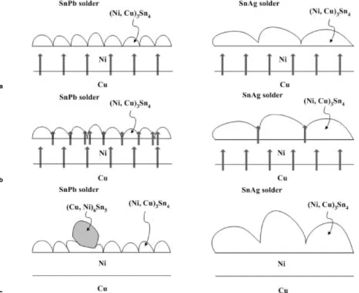
In summary, the growth of the (Ni,Cu)3Sn4 IMC and existence of (Cu,Ni)6Sn5 are the major differ-ences between the Sn-Ag system and Sn-Pb system during multiple reflows. To distinguish these varia-tions, the mechanisms of Cu diffusion and IMC transformation in these two systems should be further investigated. According to the IMC mor-phologies and related quantitative analysis, the sequence of Cu diffusion and IMC transformation could be proposed in Fig. 6. In both the Sn-Ag and Sn-Pb system, during the first cycle of reflow, Cu first diffused through columnar Ni and then dissolves into Ni3Sn4to form the (Ni,Cu)3Sn4IMC, as shown in Fig. 6a. Some Cu atoms further diffused through the (Ni,Cu)3Sn4 IMC and reacted with Ni and Sn to form (Cu,Ni)6Sn5 in the Sn-Pb/Ni
interface after more than three reflow times. How-ever, the grain sizes of the (Ni,Cu)3Sn4IMC formed in the Sn-Ag system after one reflow were larger than those in the Sn-Pb system, as indicated in Figs. 3a and 5a. The pathways for Cu diffusion in Sn-Ag system were thus reduced.
Because of the effect of Cu diffusion on the interfa-cial reaction and compound formation in the Sn-Pb system, the phase transformation between the Sn-Pb solder and Ni/Cu could be correlated to a Sn-Cu-Ni ternary equilibrium.12 However, in the Sn-Ag sys-tem, the role of Cu diffusion was not as significant because the pathway for Cu diffusion was reduced, as shown in Fig. 6b. The growth of the (Ni,Cu)3Sn4 IMC during reflows blocked the diffusion path for Cu. Thus, only the thicker Ni3Sn4IMC was revealed, and no Cu6Sn5IMC could be observed in the inter-face between Sn-Ag and Ni, as shown in Fig. 6c. The morphologies and grain-size distributions of the (Ni,Cu)3Sn4 IMC formed at the initial stage of reflow process are crucial for the subsequent phase transformation of other IMCs in the joint assembly.
Fig. 4. Cross-sectional images of the interfacial morphology in the Sn-37Pb solder/3-µm Ni joint during reflow: (a) one time and (b) ten times.
a b
Fig. 5. Top-view micrographs of the interfacial compound in the Sn-37Pb solder/3-µm Ni joint during reflow: (a) one time and (b) ten times.
CONCLUSIONS
Through appropriate etching and sample prepara-tion, IMCs of Ni3Sn4and Cu6Sn5were revealed with distinct morphologies in a solder/Ni-Cu UBM joint assembly. In the Sn-Ag system, only the (Ni,Cu)3Sn4 IMC with a faceted and particlelike grain formed in the solder/Ni interface during reflows. The thick-ness and grain sizes of (Ni,Cu)3Sn4 increased with cycles of reflow. A wavy interface was revealed after ten reflow times. In the Sn-Pb system, another (Cu,Ni)6Sn5 IMC with a rod-type grain formed on (Ni,Cu)3Sn4 after more than three reflow times. During reflow, the thickness of the (Ni,Cu)3Sn4IMC remain identical; however, the amounts of the (Cu,Ni)6Sn5 IMC increased with reflow times. Be-cause the grain sizes of the (Ni,Cu)3Sn4IMC formed in the Sn-Ag system after one reflow were larger than that in the Sn-Pb system, the pathways for Cu diffusion were reduced. It is thus argued that the Cu diffusion plays a key role in the interfacial reaction and compound transformation in the Sn-Pb system. Nevertheless, the Cu diffusion on IMC transforma-tion in the Sn-Ag system was insignificant and could
be neglected. Thus, only the thicker (Ni,Cu)3Sn4 IMC was observed, and no (Cu,Ni)6Sn5IMC could be detected between the solder and Ni.
ACKNOWLEDGEMENTS
The financial support from Taiwan Semiconductor Manufacturing Company is acknowledged. Partial support from the National Science Council under Contract No. NSC-90-2216-E007-058 is also acknowledged.
REFERENCES
1. K.S. Bae and S.J. Kim, J. Mater. Res. 17, 743 (2002). 2. H.W. Miao and J.G. Duh, Mater. Chem. Phys. 71, 255
(2001).
3. D.R. Frear, J.W. Jang, J.K. Lin, and C. Zang, JOM 53, 28 (2001).
4. B.L. Young, J.G. Duh, and B.S. Chiou, J. Electron. Mater. 30, 543 (2001).
5. M. McCormack, S. Jin, G.W. Kammlott, and H.S. Chen,
Appl. Phys. Lett. 63, 15 (1993).
6. J.H. Lau, Flip Chip Technologies (New York: McGraw-Hill, 1996).
7. G.R. Blackwell, The Electronic Packaging Handbook (Boca Raton, FL: CRC Press, 2000), pp. 4.4–4.25.
Ni/Cu Under-Bump Metallization in a Flip-Chip Package 1513
a
b
c
Fig. 6. Schematic diagrams of Cu diffusion and IMC transformation in the interface of Sn-Pb and Sn-Ag solders with Ni/Cu UBM: (a) initial stage, (b) intermediate stage, and (c) final stage. The gray arrows represent the possible diffusion paths and the amount of diffused Cu atoms.