mobilities are raised, the effective carrier mobilities easily can become limited by the source/drain contact resistance. To evaluate the contact resistance, the nc-Si:H TFTs are made with a range of channel lengths. The TFTs are fabricated in a staggered top-gate bottom source/drain geometry. Both the intrinsic and the n+- or p+-doped nc-Si:H source/drain layers are deposited at 80-MHz excitation frequency at a substrate temperature of 150◦C. Trans-mission electron microscopy of the TFT cross section indicates that crystallites of doped nc-Si:H nucleate on top of the Cr source/drain contacts. As the film thickness increases, the crystallites coalesce, and the leaf-shaped crystal grains extend through the doped layer to the channel i layer. The contact resistance is estimated by measuring IDSfor several channel lengths at fixed gate and drain voltages. The results show that the contact resistance depends on the gate voltage and that the source/drain current of these TFTs at VDS = 10 V becomes limited by the contact resistance when the channel length is less than 10 µm for n-channel and less than 25 µm for p-channel.
Index Terms—Contact resistance, nanocrystalline silicon (nc-Si:H), thin-film transistors (TFTs).
I. INTRODUCTION
I
NTEGRATED circuits made on organic polymer foils (plas-tic substrates) are under intense research and development for their desirable features of light weight, flexibility, and even deformability. However, the fabrication of circuits on organic polymer substrates usually demands process temperatures of 200 ◦C or less. To realize conformable transistor backplanes, electronic materials compatible with such ultralow process temperatures are needed. Nanocrystalline silicon (nc-Si:H)Manuscript received September 7, 2007; revised December 20, 2007. This work was supported in part by the Defense Advanced Research Projects Agency’s (DARPA) High Definition Systems (HDS) Program, by the New Jersey Commission on Science and Technology, and by the Princeton Plasma Physics Laboratory under a Program in Plasma Science and Technology Fellowship. The work of I-C. Cheng was supported in part by the National Science Council, Taiwan, R.O.C., under Contract NSC 96-2218-E-002-032 and Contract NSC 96-2120-M-002-018. The review of this paper was arranged by Editor H.-S. Tae.
I-C. Cheng is with the Department of Electrical Engineering and the Graduate Institute of Photonics and Optoelectronics, National Taiwan Univer-sity, Taipei 10617, Taiwan, R.O.C. (e-mail: [email protected]).
S. Wagner is with the Department of Electrical Engineering, Princeton University, Princeton, NJ 08544 USA.
E. Vallat-Sauvain is with the Institut de Microtechnique, Université de Neuchâtel, 2000 Neuchâtel, Switzerland, and also with the Oerlikon Solar Laboratory, 2000 Neuchâtel Switzerland.
Color versions of one or more of the figures in this paper are available online at http://ieeexplore.ieee.org.
Digital Object Identifier 10.1109/TED.2008.916766
Fig. 1. Schematic cross section of the staggered top-gate bottom source/drain TFT on top of an intrinsic nc-Si:H seed layer, including layer thicknesses, materials, and functions.
is one of the candidates based on the following properties: 1) high-electron field-effect mobilities compared with a-Si:H; 2) capability of p-channel operation [1]; 3) compatibility with low process temperature; 4) compatibility with present indus-trial standard a-Si:H technology; and 5) insensitivity to light-induced defect generation [2]. nc-Si:H thin-film transistors (TFTs) with electron field-effect mobilities of 100 cm2·V−1·s−1 and higher have been reported [3]. However, as the intrinsic carrier mobilities are raised, the effective carrier mobilities easily can become limited by the source/drain contact resistance [4]. The nc-Si:H consists of a crystalline phase embedded in an amorphous matrix. If the amorphous phase lies in the current path, it may introduce undesirable source/drain contact resis-tance in the TFTs [5]. The properties of the crystalline phase depend strongly on the process conditions and the substrate type, and they evolve with film thickness [6], [7]. We evaluated the source/drain contact resistance of the nc-Si:H TFTs made with a range of channel lengths L by extrapolating plots of total resistance versus channel length to L = 0. To investigate whether the amorphous phase plays a role in determining the source/drain resistance, we studied the TFT cross sections of the channel region and of the source/drain contact regions by transmission electron microscopy (TEM).
II. EXPERIMENTS
To reduce the complexity of TFT fabrication and TEM sample preparation, all devices described in this paper are made on Corning 1737 glass substrates at a temperature that Kapton E polyimide substrates can tolerate.
The nc-Si:H TFTs are fabricated in the staggered top-gate bottom source/drain geometry on top of a nc-Si:H seed layer as shown in Fig. 1. The top gate is used to take advantage
Fig. 2. UV reflectance spectra of nc-Si:H samples with hydrogen dilution ratios of (a) 20 and (b) 30 deposited at various substrate temperatures. For easy comparison, the curves were shifted along the reflectance axis by: (a)−0.06 for 190◦C,−0.03 for 150◦C, and−0.09 for 120◦C and (b) +0.12 for 150◦C, +0.04 for 120◦C, and−0.10 for 90◦C.
of the highest carrier mobilities available in the nc-Si:H films. The bottom source/drain geometry is introduced to avoid the channel overetch that is usually encountered in fabricating the conventional coplanar top source/drain geometry. First an
∼60-nm-thick intrinsic nc-Si:H seed layer is deposited by
plasma-enhanced chemical vapor deposition (PECVD), be-neath the whole TFT structure, to promote rapid nucleation of the channel layer. We intentionally build the seed layer such that the crystallites do not yet coalesce. This seed layer suffices to promote crystallinity in the channel but does not conduct well electrically, with a room-temperature dark conductivity of 3.6× 10⁻¹² S· cm−1, which avoids introducing a low shunt resistance that may produce a high OFF current. On top of the seed layer is∼50-nm-thick evaporated Cr for the bottom source/drain electrodes, followed by an∼50-nm-thick PECVD n+ nc-Si:H source/drain contact layer. The source/drain pat-terns are defined by dry etching of the n+ nc-Si:H layer and wet etching of the Cr layer. Then, an∼50-nm-thick intrinsic nc-Si:H and an ∼300-nm-thick SiO2 layer are deposited as channel and gate dielectric layers, respectively. After the con-tact holes are opened by wet chemical etch and dry plasma etch, an∼200-nm Al layer is thermally evaporated and patterned into source, drain, and gate.
To minimize the OFF current and maximize the ON/OFF
current ratio, we want the intrinsic nc-Si:H channel film to develop high crystallinity in a thin layer. The intrinsic nc-Si:H films are deposited from a gas mixture of hydrogen, silane, and dichlorosilane (DCS) at an excitation frequency of 80 MHz, an absorbed power of 86 mW/cm2, and hydrogen dilution ratios of Ri= [H2]/[SiH4+ SiCl2H2] ranging from 20 to 30. The very high excitation frequency ensures a good film crystallinity. The addition of 20–30 vol.% DCS to silane compensates the film from n-type to intrinsic [8]. Two bands in the ultraviolet reflectance spectra at 276 and 365 nm indicate the crystallinity of the films [9], [10]. Fig. 2 shows that films grown at higher hydrogen dilution ratio have higher crystallinity and that the crystalline volume fraction first increases and then decreases when the deposition temperature is varied from low to high at otherwise fixed deposition conditions. The room-temperature dark conductivity of an ∼300-nm-thick intrinsic nc-Si film deposited at 150◦C is ∼6 × 10⁻⁷ S· cm−1 for Ri= 20 and
∼3 × 10⁻⁶S· cm−1for R
i= 30.
The desired properties for the n+- or p+-doped nc-Si:H layer are the following: 1) high conductivity for low source/drain contact resistance; 2) sufficient crystallinity to promote the nucleation of the channel layer in the staggered bottom source/drain TFT geometry; and 3) sufficiently thin to en-sure step coverage in the following transistor fabrication. The doping of the PECVD nc-Si:H is achieved by introducing phosphine (PH3) or diborane (B2H6) into the hydrogen-diluted silane source gas. The deposition parameters are a pressure of 500 mtorr, an absorbed power of 103 mW/cm2, and hydro-gen dilution ratios of Rp= [H2]/[SiH4+ B2H6] =∼200 for p-type and Rn= [H2]/[SiH4+ PH3] = ∼88 for n-type. Be-cause the dopants are detrimental to film crystallinity, high hydrogen dilution ratios are required to obtain the nanocrys-talline phase. As functions of deposition temperature at otherwise fixed deposition conditions, the sheet resistance, the room-temperature conductivity, and the dopant concentration are measured in n- and p-type nc-Si:H films. Fig. 3 shows that the highest conductivities of ∼16 and ∼1 S · cm−1 are reached at the deposition temperatures of∼200◦C for n-type and∼150◦C for p-type, respectively. The decrease of doping efficiency at deposition temperature higher than 200◦C results from the reduction of film crystallinity.
To ensure compatibility with plastic substrates, adequate crystallinity of the intrinsic nc-Si:H channel films, and suffi-cient conductivity of the doped nc-Si:H films, we chose the temperature of 150 ◦C for the PECVD nc-Si:H deposition in TFT fabrication.
III. RESULTS ANDDISCUSSION
A. Analysis of TFT Contact Resistance
The TFT characteristics were evaluated with an HP 4155A parameter analyzer. Because the mobility value shows a de-pendence on gate voltage, the effective field-effect mobility is determined by the maximum of the average slope of the transfer curve taken over the local five adjacent points versus the gate voltage. The TFTs shown in Fig. 4 have a hole field-effect mobility of∼0.35 cm2· V−1· s−1for channel width-to-length ratio of W/L = 180 µm/30 µm and an electron field-effect mobility of 43 cm2· V−1· s−1for W/L = 160 µm/40 µm.
Fig. 3. (a1) Sheet resistance and (a2) room-temperature conductivity and phosphorus concentration in the n-type nc-Si:H films on seed layers as functions of deposition temperature. The films were deposited from a gas mixture of SiH4:PH3= 12.5 : 1 with a hydrogen dilution ratio of 88. (b1) Sheet resistance and
(b2) room-temperature conductivity and boron concentration in the p-type nc-Si : H films on seed layers as functions of deposition temperature. The films were deposited from a gas mixture of SiH4: B2H6= 40 : 1 with a hydrogen dilution ratio of 200. The phosphorus and boron concentrations were obtained from the
secondary ion mass spectrometry measurements. The lines are guides to the eye.
Fig. 4. Transfer characteristics of the p- and n-channel nc-Si:H TFTs fabri-cated at 150◦C in a staggered top-gate bottom source/drain geometry. The channel dimensions are W/L = 180 µm/30 µm for p-channel and W/L = 160 µm/40 µm for n-channel. The TFTs have a hole mobility of∼0.35 cm2·
V−1· s−1and an electron mobility of∼43 cm2· V−1· s−1.
When the intrinsic carrier mobilities are raised, the effective carrier mobilities may become limited by the contact resistance. The resistance can be estimated from the measurements of
IDS for several channel dimensions at fixed VDS and VGS. The total resistance from source to drain RTOT= VDS/IDS consists of the following: 1) the contact resistance R0, which
is inversely proportional to W , and 2) the channel resistance
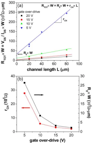
RCH= rCH× (L/W ), where rCH is the channel resistance per L/W . The contact resistance is determined from the in-tercept with the Y -axis when RTOT× W (Y -axis) is plotted versus L (X-axis) and the slope denotes rCH. We define a critical channel length, at which the source/drain current limita-tion sets in, when the contact-resistance contribulimita-tion R0× W is equal to the channel-resistance contribution rCH× L. An n-channel example is shown in Fig. 5(a). We investigate the contact resistance at various gate overdrive voltages VGS− Vth. Fig. 5(b) shows that the contact resistance depends on the gate overdrive voltage when the TFTs are operated at VDS= 10 V. In this particular case, R0× W decreases from 26.4 × 10⁶to 2.2× 10⁶ Ω· µm when the gate overdrive voltage increases from 5 to 20 V, and R0 limits the source/drain current at dif-ferent gate overdrive voltages when the channel length L is less than 10 µm. Fig. 6 shows a p-channel case. The considerable scatter notwithstanding RTOT× W appears to depend on the channel length and suggests that the contact resistance may dominate for channels shorter than∼25 µm.
B. TEM of the nc-Si:H TFTs
To investigate whether the amorphous phase in nc-Si:H affects device performance, we studied the cross sections of
Fig. 5. (a) Contact-resistance estimation for the n-channel TFTs with various channel dimensions operated at VDS= 10 V and four gate overdrive voltages
VGS− Vthusing a linear fit of (RTOT× W ) to L. (b) Channel resistance per
(L/W ) rCHand product of contact resistance and channel width R0× W
at four gate overdrive voltages. All devices have source/gate and gate/drain overlaps of∼5 µm.
Fig. 6. Contact-resistance estimation for the p-channel TFTs using a linear fit of (RTOT× W ) to L. The data points are taken from transfer
characteris-tics at VDS= 10 V and VGS− Vth≈ 20 V of TFTs with various channel
dimensions. The scatter may result from uncertainty in channel dimensions or nonuniform contact resistance. All devices have source/gate and gate/drain overlaps of∼5 µm.
TFTs in the channel region and at the source/drain contact by TEM. Fig. 7(a) shows that the doped nc-Si:H nucleates at the Cr layer and that the leaflike crystal grain extends through the doped nc-Si:H to the channel i nc-Si:H layer. This obser-vation suggests that the contact resistance between the doped
Fig. 7. Transmission electron micrographs at (a) the source/drain region of a p-channel nc-Si:H TFT and (b) the source/drain-gate overlap region of an n-channel nc-Si:H TFT. Undercut of the Cr at the source/drain-gate overlap is observed and is circled in (b).
nc-Si:H source/drain layer and the intrinsic nc-Si:H channel layer is not caused by the presence of a continuous amorphous layer at the doped-undoped nc-Si:H interface. Undercut of the Cr at the source/drain-gate overlap is shown in Fig. 7(b). X-ray photoemission-spectroscopy (XPS) analysis reveals that the cantilever, which is circled in Fig. 7(b), is a chromium oxide. This undercut is formed because the underlying Cr metal is etched faster by the Cr etchant than the oxidized surface of the Cr layer. Therefore, a top Cr–O slab survives the Cr etch. While the residual Cr–O cantilever might provide a possibly beneficial tapered source/drain edge, unwanted contamination may be trapped underneath it.
IV. SUMMARY
The dependence of film crystallinity on deposition tempera-ture and the doping efficiency of PECVD nc-Si:H thin films are investigated. An electron mobility of∼43 cm2· V−1· s−1and a hole mobility of∼0.35 cm2· V−1· s−1are demonstrated in the staggered top-gate bottom source/drain nc-Si:H TFTs made at 150◦C. TEM analysis indicates that the physical origin of the channel/source/drain contact resistance is not a poor interface between the channel and doped source/drain layers. Cr undercut is observed at the source/drain-gate overlap region. Analysis of current–voltage characteristics shows that the contact resistance decreases as the gate voltage increases. At VDS= 10 V, the
[2] V. Svrcek, I. Pelant, J. Kocka, P. Fojtik, B. Rezek, H. Stuchlikova, A. Fejfar, J. Stuchlik, and A. Poruba, “Transport anisotropy in micro-crystalline silicon studied by measurement of ambipolar diffusion length,”
J. Appl. Phys., vol. 89, pp. 1800–1805, Feb. 2001.
[3] C.-H. Lee, A. Sazonov, and A. Nathan, “High-mobility nanocrystalline silicon thin-film transistors fabricated by plasma-enhanced chemical vapor deposition,” Appl. Phys. Lett., vol. 86, no. 22, pp. 222 106-1– 222 106-3, May 2005.
[4] K.-Y. Chan, E. Bunte, H. Stiebig, and D. Knipp, “Influence of contact ef-fect on the performance of microcrystalline silicon thin-film transistors,”
Appl. Phys. Lett., vol. 89, no. 20, pp. 203 509-1–203 509-3, Nov. 2006.
[5] I.-C. Cheng, S. Wagner, S. Bae, and S. J. Fonash, “High electron mobility TFTs of nanocrystalline silicon deposited at 150◦C on plastic foil,” in
Proc. Mater. Res. Soc. Symp., 2001, vol. 664, pp. A26.1.1–A26.1.6.
[6] E. Vallat-Sauvain, U. Kroll, J. Meier, A. Shah, and J. Pohl, “Evolution of the microstructure in microcrystalline silicon prepared by very high fre-quency glow-discharge using hydrogen dilution,” J. Appl. Phys., vol. 87, no. 6, pp. 3137–3142, Mar. 2000.
[7] A. S. Ferlauto, R. J. Koval, C. R. Wronski, and R. W. Collins, “Extended phase diagrams for guiding plasma-enhanced chemical vapor deposition of silicon thin films for photovoltaics applications,” Appl. Phys. Lett., vol. 80, no. 15, pp. 2666–2668, Apr. 2002.
[8] R. Platz and S. Wagner, “Intrinsic microcrystalline silicon by plasma-enhanced chemical vapor deposition from dichlorosilane,” Appl. Phys.
Lett., vol. 73, no. 9, pp. 1236–1238, Aug. 1998.
[9] W. C. Dash and R. Newman, “Intrinsic optical absorption in single-crystal germanium and silicon at 77◦C and 300◦K,” Phys. Rev., vol. 99, no. 4, pp. 1151–1155, Aug. 1955.
[10] H. R. Philipp and E. A. Taft, “Optical constants of silicon in the region 1 to 10 eV,” Phys. Rev., vol. 120, no. 1, pp. 37–38, Oct. 1960.
Sigurd Wagner (SM’80–F’00) received the Ph.D.
degree from the University of Vienna, Vienna, Austria, in 1968.
He was a Postdoctoral Fellow with Ohio State University, Columbus, a Member of Technical Staff with the Bell Telephone Laboratories, and the Chief of the Photovoltaic Research Branch, Solar Energy Research Institute. Since 1980, he has been a Profes-sor with the Department of Electrical Engineering, Princeton University, Princeton, NJ. He is develop-ing technology for flexible and conformally shaped large-area displays, electrotextiles, and elastic electronic skin. His work in-cludes thin-film silicon on plastic and steel foils; the interdependence of elec-trical and mechanical properties in film-on-foil electronics; and the functional cells for large-area electronics, including displays, multifunctional materials, and sensor skin.
Evelyne Vallat-Sauvain received the M.S. degree
in structural metallurgy from the University of Neuchâtel, Neuchâtel, Switzerland, and the Ph.D. degree in applied physics from the Institut de Mi-crotechnique, Université de Neuchâtel in 1992.
She is currently an Associate Professor with the Institut de Microtechnique, Université de Neuchâtel. She is also with the Oerlikon Solar Laboratory, Neuchâtel. Her research interests include thin-film silicon photovoltaics and material structure analysis by transmission electron microscopy.