國 立 交 通 大 學
材 料 科 學 與 工 程 研 究 所
博 士 論 文
碳基介電薄膜的製備與其應用在 ULSI 連線技術之特性評估
Thin Film Preparation and Characterization of Carbon-based
Dielectrics for ULSI Interconnect Technology
研究生:李 延 煒
指導教授:陳 家 富 博 士
碳基介電薄膜的製備與其應用在 ULSI 連線技術之特性評估
Thin Film Preparation and Characterization of Carbon-based
Dielectrics for ULSI Interconnect Technology
研 究 生:李 延 煒 指 導 教 授 : 陳 家 富 博 士
Student : Yan-Way Li Advisor : Dr. Chia-Fu Chen
國立交通大學
材料科學與工程研究所
博 士 論 文
A DESSERTATION
SUBMITTED TO INSTITUTE OF MATERIALS SCIENCE AND ENGINEERING
COLLEGE OF ENGINEERING
IN PARTIAL FULFILLMENT OF THE REQUIREMENTS FOR THE DEGREE OF DOCTOR PHILOSOPHY
IN
MATERIALS SCIENCE AND ENGINEERING SEPTEMBER 2002
碳 基 介 電 薄 膜 的 製 備 與 其 應 用 在 ULSI 連 線 技
術 之 特 性 評 估
研 究 生:李延煒 指導教授:陳家富博士 國立交通大學 材料科學與工程研究所 博士班
中 文 摘 要
本實驗嘗試以無柵極離子束沉積法(gridless ion beam deposition, GIBD)及電漿輔助化學氣相沉積法(plasma-enhanced chemical vapor deposition,PECVD)分別製作非晶質碳及碳化矽薄膜,並且探討其漏電 流及介電常數等特性及其應用在銅製程中蝕刻阻止層的可能性評估。 首先利用 GIBD 法在常溫下以乙炔(C2H2)及氬氣(Ar)混合氣體沉積 非晶質碳膜,並加以退火及氫電漿處理來改變薄膜特性。經拉曼分析 結果顯示,ID/IG強度比及 D 特徵峰波數(wavenumber)皆隨著乙炔流量 的增加而減小,乙炔流量增加至60 sccm 時有類鑽石(diamond-like)化的 最佳條件,因此我們利用此條件所形成的 DLC 膜再分別作真空退火及 氫電漿處理,探討其對 DLC 膜之特性影響,結果顯示 DLC 膜隨著退 火溫度增加,ID/IG 強度比逐漸地增大,同時薄膜密度也由 3.44 g/cm3 減小到 2.89 g/cm3,而退火溫度從200℃至 300℃時漏電流密度會逐漸 的增大,推測此現象可能是因退火時造成薄膜中的碳逐漸石墨化所 致。另外經氫電漿處理後的 DLC 膜則隨著處理時間的增加而漏電流逐
MV/cm 的電場下),明顯低於未經處理之 DLC 膜(1×10⁻⁴ A/cm2),介電 值為3.4 也明顯低於未經氫電漿處理的 DLC 膜介電值(3.83)。 其次,利用 PECVD 法來沉積碳化矽薄膜時,以矽烷(SiH4)及甲烷 (CH4)之混合氣體作為反應氣體源,基材溫度保持在 250℃下沉積含氫 非晶質碳化矽(a-SiC:H)薄膜。並分別以薄膜測厚儀及汞探針電性量測 系統量測薄膜的厚度及介電常數,結果顯示,隨著甲烷流量的增加, 薄膜的沈積速率、折射率及介電常數皆明顯的減小。以 5%的矽烷濃度 最佳條件下所形成的碳化矽(C/Si:68/25)膜的折射率為 1.76、介電常數 為3.6、漏電流 1.79×10⁻⁸ A/cm2 (在 1MV/cm 的電場下)為最小及沉積速 率為1.32 Å/s。再將此碳化矽薄膜分別施以氫(H2)及氨(NH3)電漿表面處 理,結果經氨電漿表面處理後的薄膜除了表面粗糙度較氫電漿處理的 表面粗糙度大外,薄膜表面會形成氮化層,致使薄膜漏電流密度明顯 的降低,而經氫電漿表面處理後的薄膜表面碳含量皆隨著處理時間的 增加而減少的同時漏電流密度亦有降低的趨勢。
Thin Film Preparation and Characterization of Carbon-based
Dielectrics for ULSI Interconnect Technology
Student : Yan-Way Li Advisor : Dr. Chia-Fu Chen Institute of Materials Science and Engineering
National Chiao Tung University
ABSTRACT
The purpose of this work is research the dielectric properties of a-C and a-SiC:H films, deposited respectively by using gridless ion beam deposition (GIBD) and plasma-enhanced chemical vapour deposition (PECVD), to evaluate the possibility for using in the etching-stop layer of copper interconnect technology. Amorphous hydrogenated carbon (a-C:H) films were deposited from gas mixtures of acetylene (C2H2) and argon (Ar) in a GIBD system supplied with dc power. Vacuum annealing and hydrogen plasma treatment were performed on the a-C:H films and their effects on the physical and electrical characteristics of the films were investigated. The structure and properties of the film were investigated as functions of the C2H2 flow rate, using Raman spectroscopy. The Raman spectra revealed that the Raman ID/IG ratio and D peak position decreases with C2H2 flow rate, indicating more diamond-like character of the films. Otherwise, the annealed a-C:H films exhibited that the Raman ID/IG ratio increases with annealing temperature, but the film density decreases simultaneously, indicating more graphite-like character for the annealed films as the annealing temperature was increased. The dielectric constant of the annealed a-C:H films was reduced from 3.8 to 2.9, but the leakage
was increased from 200℃ to 300℃. However, the leakage current density and dielectric constant of the hydrogen-plasma-treated a-C:H films were clearly lower than those of the as-deposited a-C:H films.
Amorphous SiC:H films were deposited from a mixture of silane and methane gases, using PECVD. Reducing the ratio of the silane flow rate decreased the deposition rate of the a-SiC:H films, decreasing the refractive index and dielectric constant, but increasing the optical band gap and the hydrophobicity of the surface. It has a minimum refractive index (1.76), dielectric constant (3.6), leakage current density (1.79×10⁻⁸ A/cm2 at the electric field of 1MV/cm) and deposition rate (1.32 Å/s) for the concentration of silane, which is 5% in the mixture gas. XPS data indicate that the carbon concentration of the a-SiC:H films declined as the methane flow rate increased, but the silicon concentration increased. Carbon-rich films were treated with hydrogen and ammonia plasma for various periods, but were then converted into films with higher silicon content. Increasing the ammonia or hydrogen plasma treatment duration roughened the surface, even though the original film had a smooth surface, with a roughness of 0.231 nm. Ammonia plasma treated film has larger roughness (1.741 nm) than that of by using hydrogen plasma treated films (0.829 nm). The ammonia ionization species reacted with Si to promote the formation of silicon nitride. Accordingly, the leakage current density of a-SiC:H films declined as the ammonia plasma treatment time decreased, but the dielectric constant slightly increased. As expected, the leakage current density and the dielectric constant of a-SiC:H films declined as the hydrogen plasma treatment period increased.
致 謝
首先,我要向我的指導教授陳家富博士,致上誠摯的謝意與最高 的敬意。六年來在陳老師的教導下學習了許多專業領域的知識,在學 習的過程中難免遭遇挫敗,老師總能在我思考混沌時給予即時的協助 與鼓勵;在生活上從老師的身教與言教中學習到處事待人的生活哲 學,更豐富了我生命的寬度與廣度,由衷地感謝陳老師數年來的指導 與照顧。感謝和喬科技(股)公司的張志高博士等研究群,非常熱情地 提供實驗所需的過濾式電弧沉積設備與技術指導,感謝您們的幫忙與 指教。此外,感謝在台灣積體電路(股)公司工作期間,承蒙王英朗博士 的指導,使我能參與半導體製程的 CVD 鍍膜工作,真是個難得的機會。 另外亦感謝明道管理學院的汪大永校長,感謝您在我碩士階段的教 導,奠定我在真空鍍膜領域的基楚與興趣。 感謝″新素材與薄膜實驗室″所有努力的夥伴,感謝大家的協助與 勉勵,尤其是曾欲仁、徐耀斌及林琨程學長與歐耿良在學業與生活上 的討論與協助。同時也感謝毫微米實驗室的潘扶民博士的論文指導與 修改,以及孫旭昌與蔡國強工程師等研究群在 PECVD 設備與分析儀器 上的技術協助。 最後要深深感謝我的父母與研究所時的女朋友現在的老婆,沒有 先母當年對我修讀博士學位堅持,就沒有今天取得博士學位的我,感 謝您! 我的母親。更感謝老婆在這六年的時光中鼓勵我、支持我,讓 我在每遇挫折時仍能持續學習與堅持。 僅以此論文感謝在我生命中出現的您們,及許許多多的朋友與貴 人,因為您們我才能堅持不退縮,在此致上我最深深的感謝。TABLE OF CONTENTS
Abstract (in Chinese) ... ii
Abstract (in English) ... iv
Acknowledgements ... vi
Table of contents ... vii
List of figures ... ix
List of tables ... xii
Chapter 1 Introduction ... 1
1.1 Motivation of this study ... 1
1.2 Thesis outline ... 9
Chapter 2 Paper review and Fundamental Theories ... 11
2.1 Plasma-Enhanced Deposition of Film ... 11
2.1.1 Plasma Fundanmental ... 11
2.1.2 Plasma-Enhanced Chemical Vapor Deposition ... 13
2.2 Cu Metallization and Low-K Dielectrics ... 16
2.2.1 RC time delay ... 16
2.2.2 The needs of Cu metallization ... 18
2.2.3 The needs of low-K dielectrics ... 19
2.2.4 The needs of Cu Diffusion Barriers ... 23
Chapter 3 Effect of Post-treatment on Electrical Properties of Amorphous Hydrogenated Carbon Films Deposited by Gridless Ion Beam Deposition ...32
3.1 Introduction ... 32
3.2 Experimental ... 34
3.3 Results and discussion ... 36
3.4 Conclusions ... 44
Chapter 4 Effects of Ammonia Plasma and Hydrogen Plasma Treatment on the Electrical Properties of PECVD Amorphous Hydrogenated Silicon Carbide Films ... 55
4.1 Introduction ... 55
4.2 Experimental ... 57
4.3.2 Effects of ammonia plasma and hydrogen plasma
treatment on the a-Si0.28C0.65:Hy films ...66
4.4 Conclusions ...72
Chapter 5 Conclusions and future work ... 98
References ... 102
LIST OF FIGURES
Fig. 2.1 Plasma chemistry of the hydrogen molecule as the
impinging electron energy in increased....26
Fig. 2.2 Schematic representation of the plasma-enhanced CVD
reaction process....27
Fig. 2.3 Calculated delays for Al/SiO2 and Cu/Low-K
interconnect systems. ... 28 Fig. 2.4 Integration of Cu and low-K dielectrics into a dual
damascene architecture. ... 29 Fig. 3.1 Metal-insulator-semiconductor (MIS) structure... 46 Fig. 3.2 The fitted curves of Raman spectra of the a-C:H films... 47 Fig. 3.3 Graphs of (a) Raman ID/IG ratio, and (b) D-peak
position of a-C:H films as a function of C2H2 gas flow rate... 48 Fig. 3.4 Raman spectra of the a-C:H films with different
annealing temperatures, (a) 100℃, (b) 200℃, (c) 300℃, and (d)
400℃... 49 Fig. 3.5 Graphs of (a) Raman ID/IG ratio and (b) D-peak position
of a-C:H films with various annealing temperatures in vacuum. ... 50 Fig. 3.6 Density of a-C:H films for various vacuum annealing
temperatures. ... 51 Fig. 3.7 J-E curves of a-C:H films with different vacuum
annealing temperatures. ... 52 Fig. 3.8 (a) Dielectric constant (K) of a-C:H films with different
vacuum annealing temperatures, and (b) Dielectric constant of
Fig. 3.9 J-E curves of a-C:H films with different hydrogen
plasma treatment. ... 54 Fig. 4.1 Schematic diagram of the PECVD system. ... 74 Fig. 4.2 Deposition rate of a-SimCn:Hy films as a function of x
value [x = SiH4/(SiH4)+(CH4)]. ... 75 Fig. 4.3 Optical energy gap (Eg), and refraction index (n) of
a-SimCn:Hy films as a function of x value [x =
SiH4/(SiH4)+(CH4)]... 76 Fig. 4.4 Dielectric constant (K) of a-SimCn:Hy films as a
function of x value [x = SiH4/(SiH4)+(CH4)]. ... 77
Fig. 4.5 IR spectra of the a-SimCn:Hy films of different methane
flow rates. ... 78 Fig. 4.6 ESCA spectra of the near surface region of a-SimCn:Hy
films with various methane flow rate, (a) 35 sccm, (b) 50 sccm,
(c) 70 sccm, and (d) 100 sccm. ... 79 Fig. 4.7 The composition of the near-surface region of the
a-SimCn:Hy films with various methane flow rate, analyzed by
ESCA... 80 Fig. 4.8 The water contact angle and the dispersive component
of the free energy of the a-SimCn:Hy films as a function of
methane flow rate... 81 Fig. 4.9 The surface roughness of a-SimCn:Hy films with various
films thickness, (a) 10 nm, (b) 50 nm, (c) 100 nm, and (d) 150
nm... 82 Fig. 4.9(e) The surface roughness of a-SimCn:Hy films with
various films thickness... 83 Fig. 4.10 Dielectric constant (K) of a-SimCn:Hy films with
ammonia plasma treatment periods, (a) 0 min, (b) 5 min, and (c) 20 min, and (d) AFM roughness of a-SiC:H films with various
plasma treating periods. ... 85 Fig. 4.12 AFM images of hydrogen plasma treated a-SiC:H
films with varies hydrogen plasma treatment periods, (a) 5 min,
(b) 15 min, and (c) 20 min. ... 86 Fig. 4.12 (d) Roughness of plasma treated a-SiC:H films with
varies hydrogen plasma treatment periods... 87 Fig. 4.13 XPS spectra of Si 2p binding peaks for the
a-Si0.28C0.65:Hy films with various ammonia plasma treatment
periods. ... 88 Fig. 4.14 The content of a-Si0.28C0.65:Hy films with different
ammonia plasma treatment period....89
Fig. 4.15 FTIR absorption spectra of a-SiC:H films for various
hydrogen plasma treatment periods....90
Fig. 4.16 The outmost layer content of a-SiC:H films with
various hydrogen plasma treatment periods....91
Fig. 4.17 J-E characteristics of a-Si0.28C0.65:Hy films before and after ammonia plasma treatment and a-SimNn:Hy films, (a) a-SimNn:Hy, (b) a-Si0.28C0.65:Hy, and with various plasma
treating periods, (c)5 min, (d)10 min, (e)15 min, and (f) 20 min. ... 92 Fig. 4.18 J-E characteristics of a-SiC:H films before and after
hydrogen plasma treatment and a-SiN:H films, (a) a-SiN:H, (b) a-SiC:H, and for various plasma treatment periods, (c) 5 min, (d)
10 min, (e) 15 min, and (f) 20 min... 93 Fig. 4.19 Dielectric constant (K) of a-Si0.28C0.65:Hy films with
LIST OF TABLES
Table 2.1(a) Dielectric constant of several materials... 30 Table 2.1(b) Some recent promising low-K materials. ... 31 Table 4.1 Deposition parameters, hydrogen/ammonia plasma
treatment parameters, and characteristics of the a-SiC:H films. ... 95 Table 4.2 Frequencies of IR peaks and assignments... 96 Table 4.3 The dielectric constant (K) of a-SiC:H films for various
Chapter 1
Introduction
1.1 Motivation of this study
Carbon-based materials generally have a high hardness, a low friction coefficient, a large refractive index, a wide band gap, a high breakdown electric field, and extremely high thermal conductivity. Therefore, such materials have considerable potential for use wear-resisting, electronic and optoelectronic applications. Our laboratory has achieved much in the field of fabricating and applying diamond and amorphous carbon (a-C) films.[1-4] Carbon-based thin films have recently attracted much attention due to carbon’s unique range of bonding configurations sp1, sp2 and sp3 and its ability to exhibit a wide variety of properties, from those of graphite to diamond. Among these materials, hydrogen-free tetrahedral a-C films have attracted special interest due to their many sp3 bonded carbon atoms, more than those of other a-C coatings, which lead to many powerful properties, such as extreme hardness, optical transparency, good electrical insulation and biocompatibility.[5-7] Our previous studies [5,6] have demonstrated that a-C films could be deposited by physical vapor deposition (PVD), and they are characterized by extreme hardness and
The wide range of applications of silicon carbide (SiC) thin films in optoelectronics (such as light-emitting diodes, color displays, and other devices) and high-temperature electronic devices (such as hetero-junction bipolar transistors, photovoltaic cells, and others) has attracted a lot of scientific interest. Besides, their chemical inertness, transparency over a broad range of wavelengths and hardness allow SiC thin films to be used in heat-sinks, optical filters, antireflection hard coatings, X-ray masks and corrosion-resistant materials. Furthermore, SiC films can also be used as a thin buffer layer in the growth of diamond films on silicon.[8] Silicon carbide films deposited by various methods and on different substrates have therefore been the subject of extensive research during the last few years.[9-15]
The physical and chemical properties of the films depend primarily on the deposition technique used. Traditional PVD processes, such as magnetron sputtering, which is used on a broad scale in wear tool coatings, fail to make smooth and continuous layers in the manufacturing of ultra-thin films.[16] The most success has been achieved using ionized PVD. The flux of sputtered or evaporated neutral atoms experiences in-flight ionization and subsequent acceleration in an electrical field, straight toward the surface of the wafer. Ion beam deposition and vacuum arc deposition may be candidate plasma sources
for ionized PVD because the self-ionization in the process generates the plasma required for directional deposition much more effectively.[17] The use of the bias voltage is to produce an additional ion bombardment at the substrate without influencing the other process parameters. The consequences of the ion bombardment effect are an increase in film density, inhibition of a columnar film growth, an improvement in adhesion, an increase of residual stress, and a change in the micro-hardness. McKenzie [18] suggested that filtered arc deposition should be a useful method of accessing high-compressive-stress regimes because of its narrow and controllable energy distribution and high flux rates. Newer developments, such as the vacuum arc-based deposition of a-C films, are becoming increasingly important. Much interest has been shown in the use of tetrahedral a-C films, deposited by filtered arc deposition, in the fabrication of electronic devices.[19-23] Recent developments have shown that effective plasma filtering techniques, using curved magnetic ducts to separate the plasma from the particles, can effectively suppress the deposition of droplets on the substrates at a reasonable deposition rate.[24,25] Unfortunately, the macro-particle filter reduces the deposition area and greatly complicates the use of the vacuum arc method for coating substrates. So far, the method has not been considered for semiconductor manufacturing since the deposition area and the
emission of microscopic liquid metal droplets from the plasma source remain outstanding issues. Besides, gridless ion beam deposition is a combination of ion implantation and physical vapor deposition (PVD), in which energetic ion bombardment is used to synthesize high-quality film materials. In this technique, the deposition is energetic; restated, the carbon species arrives with an energy significantly greater than that represented by the substrate temperature. The resultant films are dense, transparent, insulating, amorphous and display a high degree of sp3 character.[26] Therefore, one of the aims of this work is to prepare a-C:H films deposited by the GIBD system and then to perform vacuum annealing treatment and hydrogen plasma treatment to investigate the influence of the treatments on electrical properties of the films.
Chemical vapor deposition (CVD) techniques for growing carbon films have been developed in recent years,[27,28] opening up a wide field of applications of carbon films. Chemical vapor deposition offers excellent uniformity and additional degrees of flexibility; depending on the temperature of the sample, the gas dynamics and the surface composition of the substrate. The resulting films are characterized by highly aspect ratio. Among the reasons for growing films using CVD methods is the capacity to produce a wide range of films and metal coatings, and semiconductors in either a crystalline or
amorphous form, with high purity and desirable characteristics. Krishna [29] demonstrated that hydrogenated amorphous carbon (a-C:H) thin films deposited by radio-frequency plasma-enhanced CVD (PECVD), exhibit a lowest defect density. Since carbon-based films are relatively new materials, the electrical properties of semiconductive carbon-based films have received extensive attestation. Carbon-based films can be synthesized in a low-pressure and low-temperature CVD process and are widely expected to be adopted for sub-100 nm IC technology.
The manufacturing of the interconnect system in an integrated circuit represents one of the key processes in the semiconductor industry. Current technology integrates up to seven levels of high-density wiring for leading-edge logic chip applications, such as microprocessors. The decreasing feature size and the increasing complexity of the global wiring introduce signal delays, related to the increasing resistance of the longer metal lines, and the capacitance between them. The wiring and the gate RC delays have become equally important in limiting the maximum speed of the integrated circuit. Accordingly, we have seen a dramatic acceleration of research and development on low-K dielectric materials and copper metallization, to further reduce wiring RC delays. [30] Copper is now replacing aluminum as the main conducting material for all types
of integrated circuits in sub-180 nm technology nodes. Copper has a significantly lower electrical resistivity than aluminum (ρCu = 1.7 μΩ, ρAl = 2.65 μΩ) and is much more resistant to electromigration, a common problem that affects the reliability of aluminum metal lines.[31] In metallization process, dielectric films, made of inorganic material, include amorphous fluorinated carbon (a-C:F), fluorosilicate glass (FSG), dielectric SiO2 and SiN deposited by PECVD. The films, a-C:F,[32,33], FSG,[34,35] and fluorine-doped siliconoxide (SiOF),[36,37] have recently received considerable attention as potential inter-metal dielectric materials of low permittivity (K). The incorporation of fluorine, which has a high electronegativity (4.1) and reduces the polarizability of the overall network, typically reduces the refractive index and dielectric constant of the thin films.[37,38] At high temperatures, however, the diffusion of fluorine is enhanced and can interfere with the surrounding layers. The fluorine in the fluorinated dielectric layer can diffuses to accumulate at the interface.[39] The fluorine content at the interface greatly enhances Cu-Si intermixing, since fluorine atoms in the interface create silicon dangling bonds and weakly positively charged silicon atoms.[40,41] Therefore, Cu atoms may significantly penetrate into the fluorinated dielectric during heating. A diffusion barrier must be used to prevent copper atoms from diffusing into the fluorinated
dielectric. Silicon nitride (SiN) films exhibit good barrier response to copper diffusion, etching selectivity to oxides, high dielectric, mechanical and chemical stability and electrically insulating characteristics. They are essential for the semiconductor industry to surround silicon integrated circuits, and as diffusion barriers against H2O and metal ions,[42] as passivation films, [43] as gate and capacitor dielectrics.[44] However, silicon nitride suffers from a high dielectric constant of ~ 7.2.[45] This high dielectric value increases the overall inter-layer dielectric (ILD) time delay. Consequently, silicon nitride must be substituted for a barrier material with a lower dielectric constant.
SiC has been much investigated as a potential new material for use in micromechanics and high-temperature microsensors,[46] and many researchers have recently studied amorphous hydrogenated silicon carbide (a-SiC:H) as a new low-K dielectric material for use as an etch stop layer in copper metallization.[47,48] The majority of previous investigations of amorphous hydrogenated silicon carbide (a-SiC:H) films have concentrated on the use of the glow discharge PECVD technique, using alkane sources such as methane (CH4), acetylene (C2H2) and ethylene (C2H4), as carbon precursors and silane (SiH4) as the silicon source.[49-54] Besides, some researchers also used a high-density plasma (HDP) CVD system, to prepare a-SiC:H films and study
their characteristics.[48] However, the electrical properties of low-temperature deposited carbon-based films have rarely been investigated despite the fact that numerous studies of details of the electrical properties of carbon-based films have been conducted. The current leakage characteristics of conventional SiC involve its conduction through silicon. Si has an electronic polarizability 20 times that of carbon. Consequently, substituting the less polarizable carbon atoms for silicon in SiC should yield a lower dielectric constant than that of SiC. Nevertheless, these low-k materials, that contain Si-H groups, easily react with moisture to increase their leakage current and dielectric constant. The films has limited applicability at present. The hydrogen content is well known to increase with the amount of carbon,[55,56] and hydrogen plays a role in passivating the dangling bonds in the films. Dangling bonds can then easily react with moisture to form -OH bonds during the exposure of the dielectric films to the atmosphere, increasing the dielectric constant and the leakage current of the films. Consequently, hydrogen plasma treatment can be used for providing hydrogen atoms to passivate the surface and reduce the density of dangling bonds. The leakage current of hydrogen silsesquioxane (HSQ) decreases as the hydrogen and ammonia plasma treatment duration is increased.[57] Ammonia gas is commonly use as the depositing source of a-SiN films in PECVD and the
ammonia plasma generates various ionized species such as NH++, N2+ and H.[58] Liu et al. described how the passivation layer, following ammonia plasma treatment, effectively reduced the moisture uptake and the lengths of the diffusion paths of copper penetration through HSQ.[59]
This work prepares a carbon-based thin film with a lower dielectric constant than the silicon nitride film, which greatly impedes Cu diffusion and has a high chemical stability. The interaction of the copper electrode with the dielectrics was examined by making electrical measurements, using metal-insulator- semiconductor (MIS) structures.
1.2 Outline of Thesis
This dissertation is divided into seven chapters.
Chapter 1 introduces the general background to, and motivation for the growth of carbon-based films by PVD and CVD, and their applications in Cu metallization.
Chapter 2 describes the reactive mechanism and the deposition behavior associated with the plasma-enhanced deposition of films. The introduction of Cu metallization for applications in multilevel interconnect architecture also described.
deposit amorphous hydrogenated carbon (a-C:H) films. The effects of annealing and hydrogen plasma treatment on the electrical properties and the structure of a-C:H films are discussed.
Chapter 4 describes the characteristics of PECVD carbon-rich a-SiC:H films and the effects of deposition parameters on the films’ electrical properties. The effects of hydrogen and ammonia plasma treatment on the electrical and the surface properties of carbon-rich a-SiC:H films are also discussed.
Chapter 5 summarizes all experimental results and provides suggestions for future work.
Chapter 2
Paper review and Fundamental Theories
2.1 Plasma-Enhanced Deposition of Film2.1.1 Plasma Fundanmental
The use of plasma provides many advantages. For instance, energetic charged particle collisions can produce meta-stable species (such as redicals), new reaction paths and control of film microstructure and mechanical properties can be enhanced through ion bombardment, and directionality in film deposition and etching can be achieved through the acceleration of charged species in a directional potential gradient.
We consider the fundamentals of plasma chemistry by focusing on the interactions between electrons, ions, and neutrals in a discharge. Let us begin with a definition:
The plasma is a quasi-neutral gas of charged and neutral particles, which exhibits collective behavior.
Any body of gas typically contains three species: neutral atoms or molecules, ions, and electrons. Their relative concentrations (i.e., the degree of ionization) are considerably different in plasma. From the relative inefficiency of energy transfer through elastic collisions between electrons and ions or
neutrals, the inelastic processes were important for the coupling of an external power supply to sustain the plasma. The energetic of the inelastic processes depend to a great extent on the energy levels intrinsic to the gas species.
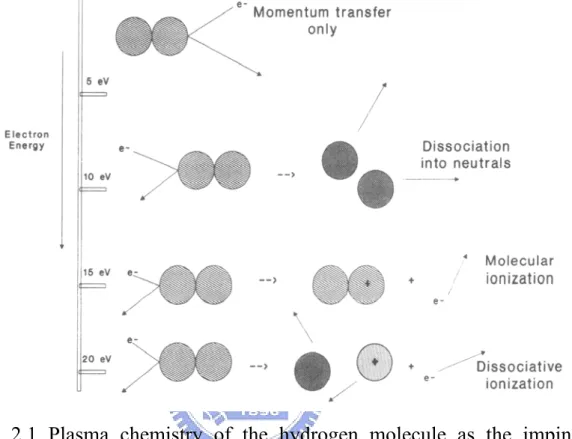
Five fundamental inelastic processes account for the majority of chemical processes occurring in plasma: (a) ionization, (b) excitation, (c) relaxation, (d) dissociation, and (e) recombination. Many other processes that occur in discharges are species dependent. All five fundamental processes can be found in the plasma of hydrogen as the energy input to the plasma is gradually increased. To illustrate the fundamental inelastic processes, following the plasma chemistry of hydrogen in a hypothetical situation where all electrons have equal energies and this energy can be gradually increased.[1]
At low energies, electron-H2 collisions are elastic and electrons suffer only momentum changes as shown in Fig. 2.1. The H-H bond strength is approximately 4.5 eV so we would expect atomic hydrogen to be formed when the electron energy is increased to this level. However, the cross section for this process is small and the mechanism requires the hydrogen molecule to be raised to an excited state. This excitation occurs at an energy of about 9 eV. Above this energy, electron impact results in the dissociation of the molecule to form two hydrogen atoms with each of them having a significant kinetic energy. The
ionization potential for H2 molecules to form positive hydrogen ions is 15.4 eV. At this energy, significant formation of singly ionized hydrogen molecules is seen. As the energy of electrons is increased further, an excited state for the positive hydrogen ion is reached, resulting in the formation of an H/H+ pair. The hydrogen atoms produced have their own excited states, which can be achieved through collisions with other atoms, ions, or electrons. In a typical glow discharge the electron energy distribution is Maxwellian, so all these processes can occur concurrently in the discharge.
2.1.2 Plasma-Enhanced Chemical Vapor Deposition
The rapidly rising applications of plasma-CVD technology have led to considerable in research on the area of basic reaction mechanism. Techniques that permit deposition of films with thickness less than 1 µm have been developed. PECVD can produce thin film of a thickness below 0.1 µm with an excellent integrity and uniformity.
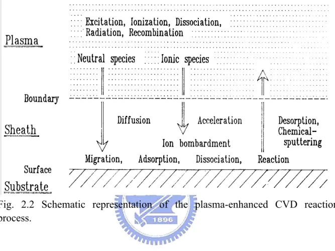
Reaction mechanisms involved in the film formation in plasma-enhanced CVD are not yet well understood, due to the complexities of the reaction system, i.e., (1) the cold plasma is not in thermal equilibrium, (2) gases used in the process are sometimes poly-atomic molecules, and (3) lack of basic data such as reaction cross sections. Furthermore, gas phase reactions in the plasma and
surface reactions on the substrate may all contribute to the film formation process. Figure 2.2 shows the reaction process in the film formation schematically. Gas molecules are excited, ionized or dissociated in the plasma mainly by electron impact. Thus excited molecules, atoms, radicals, molecular and/or atomic ions are produced and travel through the sheath layer to reach the substrate surface. The flow of reaction gases and the configuration of the electrodes and the substrate holder all affect the spatial distribution of the particle density. Particles reaching the substrate surface migrate and find adsorption sites on the surface. Finally, the surface species react with each other, resulting in the film formation. Dissociation of molecules during adsorption may also occur. The surface bombardment by ions accelerated in the sheath affects surface reactions and film properties.
In typical CVD processes, films are formed purely through thermo-chemical reactions at the substrate surface. The reaction proceeds under a nearly thermodynamic equilibrium condition. On the other hand, plasma-enhanced CVD is a film formation process that causes excited species to react with each other. This makes it possible to deposit films at lower substrate temperatures than a thermal CVD process, in which a high substrate temperature is necessary to overcome the activation energy. In order to produce the cold
plasma, low pressure is of course required. Plasma-enhanced CVD is, however, a film formation process that includes which includes chemical reactions. Therefore, high densities of active species are required in order to get higher deposition rates. The pressure ranges in plasma-enhanced CVD lies between 0.1 and 10 Torr. Mean-free paths of gas particles at this pressure range are as short as several hundred micrometers. Most electron energies are probably in the range 0.5-10 eV and the plasma density is 109-1012 cm-3. The degree of ionization is less than 10-5. The population of free radicals is much greater than those of ions, and some radicals have much longer lifetimes. Many reactions occur among excited molecules and among ions and molecules in the plasma and the sheath layer, which complicates the film deposition mechanism further.
When the flow rate of reaction gas per unit electric power used for maintaining the plasma is relatively small, the deposition rate of the film is limited by the effective flow rate of the reaction gas. When the gas flow rate is high, the deposition rate is limited by externally supplied electric power. Although the deposition rate also changes with the substrate temperature, the dependence of the deposition rate on the activation energy is often very obvious. Occasionally, the experimental activation energy may even take a negative value when deposition rates are plotted directly against the inverse of the substrate
temperature.
Even though plasma reaction mechanisms are still not well understood, PECVD applications to film formation has moved forward rapidly because of the technological demand from industries. In principle, compounds which contain elements comprising the desired film and have a higher vapor pressure can be selected as the source gas, and any film can be deposited by plasma-enhanced CVD. Hydrides and halogenides have been widely used. Organometallic compounds can also be used as source gases. Many detailed studies have been done to correlate the deposition conditions with film properties of a-Si, Si-N and Si-O. These have already been applied to semiconductor and electronic industries for mass production.
2.2 Cu Metallization and Low-K Dielectrics
2.2.1 RC time delay
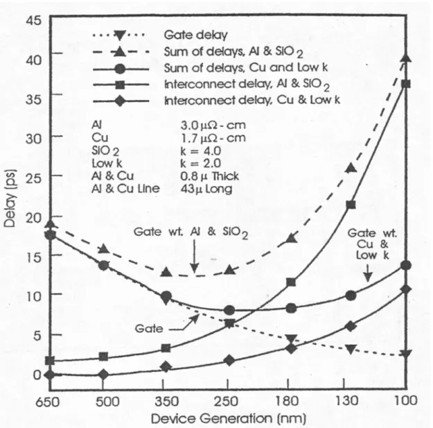
Interconnect parasitic capacitance begins to dominate the overall signal delay for integrated circuits of sub-100 nm technology, as shown in Fig. 2.3[2], and it adversely affects the packing density, reliability, and manufacturing cost of integrated circuits (ICs). Unlike transistor scaling, where performance can be improved with reduced gate length, scaled interconnects suffer from severely increased RC time delay due to higher wire resistance (R) of narrower metal
leads and higher intra/inter-level capacitance (C) between more tightly spaced interconnects. Moreover, reduced interconnect cross-sectional area also results in higher conduction current density, which exacerbates the issue of electromigration.[3] Therefore, the interconnection delay must be reduced by using new materials to alleviate the problem of achieving high performance ultra-large-scale integrated (ULSI) circuits without compromising the requirements of driving speed, crosstalk interference, and dynamic power dissipation imposed by the small feature sizes.[4]
In the high frequency (~ GHz) region, the interconnect delay within ULSI circuits is directly related to the RC time delay constant, as expressed by the following eq.: ox ox m
d
L
RC
=
ρ
ε
2where ρm: sheet resistance of the interconnect
εox: dielectric constant of the inter-metal dielectric (IMD) L: length of the interconnect
dox: thickness of the IMD
From the above equation, the RC time delay can be reduced by reducing the length of the interconnect, increasing the thickness of the IMDs, and
(low-K) IMD. Nevertheless, a longer interconnect is inevitable since both larger chip size and multilevel metallization are needed to meet the requirements of the increased functional complexity and packing density of the integrated circuits. Moreover, increasing the thickness of the IMDs would raise the concerns of planarization and via-filling. Therefore, using interconnects with a low resistivity and IMDs with low dielectric constant becomes a feasible approach for reducing the back-end RC time delay.[5-6]
2.2.2 The needs of Cu metallization
Most recently, Cu has been extensively used to substitute for the conventional Al and its alloys in deep sub-quarter-micron multilevel interconnect applications for the following reasons.[7-17]
1. Cu has a lower electrical resistivity than Al and its alloys (1.7 µΩ-cm compared to 3.0 µΩ-cm), and exhibits an excellent resistance to electro/stress-migration and hillock formation.
2. Cu can be conformally deposited into high aspect ration vias and contact holes using electrochemically deposited (ECD) as well as chemical vapor deposited (CVD) techniques, both of which inherently render much better step coverage than the currently used physical vapor deposition (PVD) methods.
3. Cu can be selectively chemical vapor deposited at fairly low substrate temperatures, thus is technically compatible with most low-K dielectrics.
4. Cu has a better thermal conductivity, higher melting point, and lower reactivity with most of the diffusion barrier materials than Al and its alloys.
Before extensive applications of Cu metallization in the Si-based ULSI circuits become feasible, however, there are many reliability issues remained to be solved. Cu is known to have a poor adhesion to most promising IMDs, and readily drifts through SiO2 at temperatures as low as 250℃ under accelerated electric field .[18-25] Moreover, Cu diffuses fast in Si and introduces deep-level traps; it also forms Cu silicides at low temperatures (200℃).[15, 25-28] Thus, the use of diffusion barriers between Cu and its underlying layers is necessary to foster adhesion and avoid Cu out-diffusion through SiO2 and/or mewly developed low-K IMDs.[29-31]
2.2.3 The needs of low-K dielectrics
With Cu successfully integrated with SiO2 in advanced sub-0.25 µm circuits for improved interconnect conductivity and reliability,[32] the process integration of Cu with low-K dielectrics can further improve IC performance by reducing the interconnect parasitic capacitance. Moreover, Cu/low-K designs in 0.13 µm technology node require only six metal levels to maintain a constant
RC, compared to 12 levels in the Al/SiO2 system.[33] More interconnect levels need more process steps, and each additional step reduces final production yield. Although Cu interconnects offer the promise of 30% faster operation speed with fewer metal levels and a lower cost of production, achieving high yields for chips with Cu interconnects remains a serious challenge, making low-K the key enabler for high performance.[34] Using low-K materials as IMDs not only ameliorates the problem of parasitic capacitance, which is dominated by the interline capacitance component in long parallel lines,[35] but also reduces the crosstalk interference between adjacent metal lines and the dynamic power consumption. Furthermore, it has been demonstrated that incorporating low-K dielectrics into multilevel interconnect is of much benefit to cost saving, as opposed to using the standard process.[36] Consequently, both performance improvement and cost saving can be achieved by using low-K materials as the IMDs.
In order to integrate new low-K dielectrics into conventional manufacturing process and to minimize the risks and costs of integration, various low-K dielectrics developed for as IMD purpose must meet stringent requirements for their electrical, physical, and chemical properties, a number of the most importance of which are listed as follows.[2,37]
1. Low dielectric constant for frequencies up to 1 GHz. (The dielectric constant of the standard plasma silicon oxide is 4.2 and values lower than this are desirable.)
2. High breakdown field strength (>2 MV/cm) and low leakage current density. (The effective resistivity should be greater than 1015 Ω-cm.)
3. Low mechanical stress (preferably compressive to weak tensile with magnitude <30 MPa.) and good adhesion to other dielectrics (oxides/nitrides) and metals (such as Ta, TaN, TiN and Cu.)
4. High thermal stability (Tg>400℃, stable up to 425℃ for short periods) and high thermal conductivity.
5. No moisture absorption or permeability to moisture. 6. No trapped charges and no sodium impurities.
7. Good thickness uniformity, step coverage, and gap filling capability, even for future 300-mm wafers.
8. Capability of being dry etched.
So far, each low-K candidate under evaluation exhibits its own attractive material properties, but no single material satisfies all the listed requirements. For example, thermal stability is one of the major concerns for the practical use of low-K dielectrics. Due to continuous high-temperature thermal cycles in the
back-end fabrication process, such as CVD-W deposition, post etching annealing, baking and curing of spin-on low-K films, and final deposition of oxides/nitrides passivation layers, it is suggested that low-K materials are preferably capable of withstanding the thermal treatment at 450℃ for at least two hours. This criterion disqualifies many prospective low-K materials for the IMD applications.[38]
Low-K (K<3.0) dielectrics are currently being extensively developed on both organic (carbon-based) and inorganic (SiO2-based) materials using both spin-on deposition (SOD) and chemical vapor deposition (CVD) techniques. Although spin-on is the most widely used method, low-K films grown by CVD are receiving widespread attention for potential back-end-of-line (BEOL) applications. Table 2.1(a) and Table 2.1(b) summarizes the dielectric constant of some materials and recent promising low-K materials for interconnect applications.[39] Three facts about the low-K material can be addressed. First, due to the fluorine-induced corrosion to metal lines, some of the low-K organic fluorinated polymers have been phased out. Second, fluorinated silicate glass (FSG) deposited either by plasma-enhanced CVD (PECVD) or by high-density-plasma CVD (HDPCVD) processes has already been integrated into BEOL applications despite its relatively high dielectric constant. In addition
to the conventional SOD, the CVD silsesquioxanes with dielectric constants below 3.0, such as methylsilane (1MS)- and trimethylsilane (3MS)-doped organosilicate glasses (OSGs),[40-44] are presently available for process development, and are expected to find widespread use. Third, there are more and more organic and inorganic porous low-K materials with dielectric constants below 2.0 under evaluation. However, the integration challenges concerning the mechanical strength, electrical reliability, and process compatibility of the porous low-K materials may defer their applications in IC manufacturing.
2.2.4 The needs of Cu Diffusion Barriers
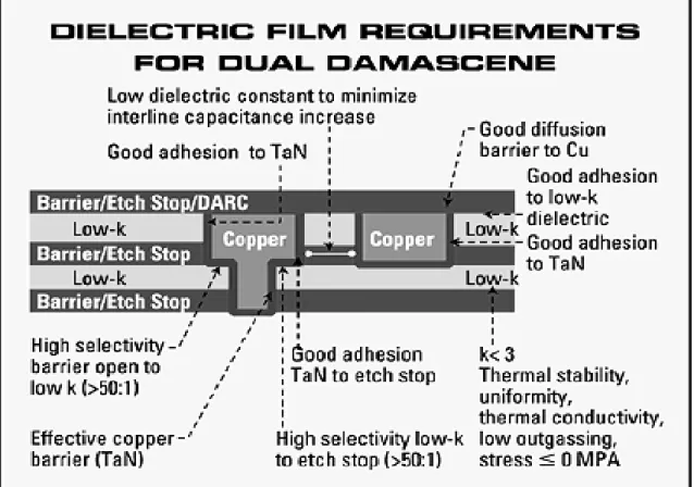
Cu is known to readily drift through most of the promising IMD materials at low temperature under accelerated electric field,[18-25] and to diffuse in Si, easily introducing deep-level traps.[15,25-28] These characteristics severely deteriorate the device’s electrical reliability, resulting in a large junction leakage, and premature dielectric breakdown. Moreover, Cu has a poor adhesion to most dielectric materials. Thus, Cu interconnect lines must be encapsulated from the surrounding dielectrics by conductive and/or dielectric barrier layers so as to foster adhesion and avoid Cu out-diffusion through the interlevel dielectric (ILD). A standard Cu dual damascene structure is shown in Fig. 2.4.[45]
must be effective against Cu out-diffusion and must be thin enough because the typical conductive and dielectric barriers have a relatively high resistivity and a high dielectric constant, respectively. These barrier films should be well adhered to the Cu layer, easily removed during Cu chemical mechanical polishing (CMP), and not reactive with Cu. Refractory metals (such as Ti, W, Ta, Cr and Mo) and their silicides and nitrides have been regarded as potential candidates for conductive barriers because of their high thermal stability, high melting points, and good electrical conductivity.[14-19,30,46-49] Specifically, Ta and TaN films deposited by PVD or CVD are the most promising materials in serving as the primary conductive barrier layer. It is well known that Ta does not alloy with Cu and that TaN possesses a dense microstructure as well as a high melting point at 3087℃. There are a number of studies on the barrier capability of Ta-based barrier layers between Cu and Si substrate as well as Cu and SiO2 dielectric. However, little work has been reported on the study of integrating the barrier layers with Cu and low-K dielectrics. As for the dielectric barriers, PECVD silicon nitride (SiN) has been the most favorable candidate because of its barrier capability against ionic impurities, moisture resistance, chemical inertness, and ease of integration. In addition to being used as a dielectric barrier against Cu diffusion, PECVD SiN has been used as an etching stop layer (ESL)
and a final capping/passivation layer in the Cu damascene structures. Nevertheless, since PECVD SiN has a high dielectric constant (K=7~9), new dielectric barriers with lower dielectric constants (such as PECVD silicon carbide) are generally used when Cu interconnects are further scaled down to the 0.13/0.10 µm nodes.[50,51]
In this thesis, we reported our study on the development of PECVD SiC:H film as the diffusion barrier for Cu interconnect technology. The barrier efficiency of thin deposited SiC:H layers in the Cu/dielectric/Si metal-insulator-semiconductor (MIS) capacitor structures is investigated using both electrical measurements and materials analyses. For comparison, the dielectric barrier capability of thin PECVD SiN films is also studied.
Fig. 2.1 Plasma chemistry of the hydrogen molecule as the impinging electron energy is increased.
Fig. 2.2 Schematic representation of the plasma-enhanced CVD reaction process.
Fig. 2.4 Integration of Cu and low-K dielectrics into a dual damascene architecture.
Table 2.1(a) Dielectric constant of several materials.
Materials
Dielectric constant
Vacuum
1.00000
Air
1.006
Silicon wafer
11.7
SiC 6H (single crystal)
9.66
Acetone
27
Water
81
Table 2.1(b) Some recent promising low-K materials.[39] Low-K material Dielectric
constant
Product name Deposition method
Supplier/source users Fluorinated SiO2 3.2-3.6 FSG PECVD or
HDP-CVD AMAT, Novellus Mattson, TEL Silsesquioxane 2.5-3.0 HOSP/LOSP FOX/HSQ Flowfill Black diamond 3MS 4MS SOD SOD CVD CVD CVD CVD AlliedSignal Dow Corning Trikon AMAT Dow Corning Schumacher/NVLS Poly(arylene ether) 2.6-2.8 SiLK
FLARE Velox SOD SOD SOD Dow Chemical AlliedSignal Schumacher Polylene 2.2-2.9 Polylene-N Polylene-AF4 CVD CVD
PRI, TI, Mattson Novellus/TI
Fluoro-Polymer 1.9-2.0 PTFE SOD Gore Fluorinated
amorphous carbon
2.0-2.6 a-F:C/FLAC CVD Novellus, AMAT NEC, Sharp MIT, UT Arlington
Diamondlike carbon 2.4-2.8 DLC CVD IBM Porous silica Mesoporous silica Porous Silsesquioxane Porous polyimide 1.2-2.3 Nanoglass - - Nanofoam - SOD SOD SOD SOD SOD AlliedSignal, TI SNL, PNNL IBM, Gatech IBM UCLA/CNXT Air-bridge 1.0
Chapter 3
Effect of Post-treatment on Electrical Properties of Amorphous
Hydrogenated Carbon Films Deposited by Gridless Ion Beam
Deposition
3.1 Introduction
Hydrogenated carbon films are produced primarily by hydrocarbon cracking. They exhibit ‘diamond-like’ properties, such as high hardness, high electrical resistivity, chemical inertness, and optical transparency.[1-3] The unique combination of these properties renders a-C:H films attractive for technological applications. In electronic applications, a-C:H can be used in place of silicon dioxide as an insulator, since its resistivity is very high. Recently, much attention has shifted towards the development of carbon-based films, deposited by plasma-enhanced chemical vapor deposition (PECVD) or high-density plasma CVD using hydrocarbon or hydrofluorocarbon precursors, to generate materials with low dielectric constants.[4-11] These unique properties in the a-C:H film may be attributed to the contained hydrogen atoms, which help to stabilize the tetrahedral bonds of carbon atoms. Increasing the proportion of tetrahedral bonds simultaneously promotes the dielectric properties of the a-C:H film.[12] Adjusting the deposition conditions, however,
was found to be able to yield a-C:H films with low dielectric constants, which make them extremely interesting for use as inter-metal dielectric layers in multiplayer metal integrated circuits.[13] Nevertheless, these films easily absorb moisture, increasing the dielectric constant and leakage current, since the dangling bonds can easily react with moisture to form -OH bonds. Choi et al.[14] suggested that in the annealing of films, the number of dangling bonds decreases as the annealing temperature increases. Hydrogen plasma treatment is also used for providing hydrogen ions with the ability to passivate the surface of the dielectric and reduce the number of dangling bonds.[15]
Gridless ion beam deposition is a combination of ion implantation and physical vapor deposition (PVD), in which energetic ion bombardment is used to synthesize high-quality film materials. One important feature of the technique is that the deposition is energetic: the carbon species arrive with an energy significantly greater than that represented by the substrate temperature. The resultant films are dense, transparent, insulating, amorphous in structure, and display a high degree of sp3 character.[16,17] Therefore, the aim of this work is to prepare a-C:H films deposited by the GIBD system, and then to perform vacuum annealing and hydrogen plasma treatment to investigate the influence of such treatments on electrical properties of the films. The electrical properties,
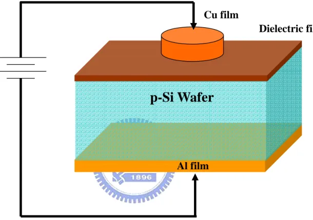
such as the leakage current density and the dielectric constant, will be evaluated with a metal-insulator- semiconductor (MIS) structure.
3.2 Experimental
One-side-polished, p-type/boron-doped 4-inch silicon wafers with resistivity of 1~10 Ω-cm and (100) orientation were used as substrates. Before the deposition, wafers were cleaned by the RCA procedure, rinsed in de-ionized water, and then dried in a nitrogen ambient. The film thickness used here was typically 300 nm and the film was deposited by GIBD at about 80℃ which involved heating by ion bombardment. The deposition source had no grid and was named “end-Hall” type ion producer.[18] The ion source was located 25 cm from the sample holder and the ions arrived with normal incidence. No bias or extra heating or cooling system was applied to the substrate. Before the deposition, the samples were sputtered by 500 eV argon beam for 10 min. High-purity (99.995%) argon (Ar) and acetylene (C2H2) were monitored by mass flow controllers and introduced separately into the deposition system. The annealing treatment of a-C:H films was carried out in vacuum for 1 h at 100, 200, and 300℃ respectively. Otherwise, the pressure for the hydrogen plasma treatment of post-deposited a-C:H films was set by the PECVD system at 300 mTorr and the plasma treatment period was 1, 3, and 6 min, respectively. The
substrate temperature was maintained at 250 ℃ , and the rf power was maintained 100 W and the hydrogen gas flow was fixed at 400 standard cubic centimeter per minute (sccm).
The refractive index and thickness of the a-C:H films were determined by the n&k Analyzer 1200. The film density was calculated from the geometrical thickness and the mass/cm2, which determined by Rutherford backscattering spectrometry (RBS) of 2-MeV He+ ions. Raman spectroscopy is probably the most common technique used for evaluation of carbon films because of its ability to distinguish between different forms of carbon. The microstructure and quality of the a-C:H films were determined by the Renishaw micro-Raman spectroscopy system 1000. Raman measurements were performed at 514.5 nm at 1 cm-1 resolution; integration times were 3 min at 50 mW Ar ion laser power. In order to investigate the dielectric properties of a-C:H films, a MIS capacitor was employed to carry out the electrical measurements, as shown in Fig. 3.1. Circular metal insulator silicon structures were fabricated by sputtering aluminum through a shadow mask onto the dielectric films. A 1-μm-thick copper film was sputtered on the wafer back surface for a good substrate contact. After copper film was deposited, the samples were annealed in a nitrogen ambient at 200℃ for 30 min. The leakage behavior was measured by
applying a staircase voltage ramp using an HP 4156B semiconductor parameter analyzer, for which the MIS capacitor was biased at accumulation polarity. Leakage current-voltage (I-V) measurements were performed to investigate the leakage properties. The high-frequency capacitance-voltage (C-V) measurements were performed at 1 MHz using a HP 4280A C-V meter. The dielectric constant was estimated from the capacitance in the accumulation region of the MIS sample and the film thickness.
3.3 Results and Discussion
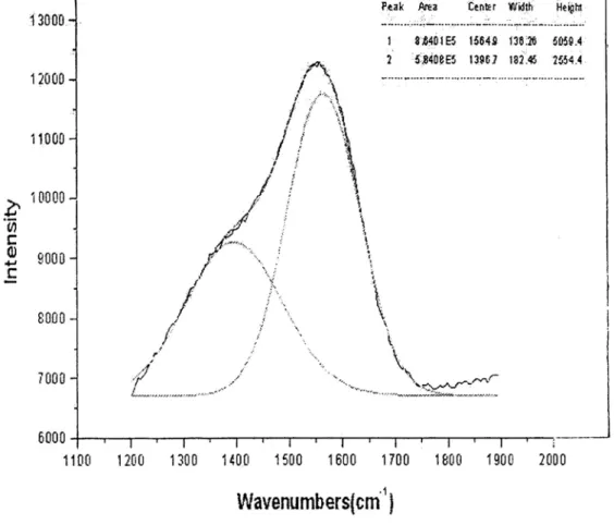
Amorphous carbon generally is considered to include a mixture of sp3 (diamond-like) and sp2 (graphite) bonding structures, in which the bond angles are no longer the ideal values of 109°28’ and 120°. Accordingly, the shape and peak positions of the corresponding Raman spectra may be different. The spectra can generally be deconvoluted into Gaussian or Lorentzian peaks at approximately 1550 cm-1 (G peak) and 1355 cm-1 (D peak), as shown in Fig. 3.2. Single-crystal graphite exhibits a Raman spectrum with a single line at 1580 cm-1, while crystalline diamond gives a single sharp line at 1332 cm-1. The literature generally splits these into a graphite or G peak at 1580 cm-1 for crystalline graphite or a band around 1450-1500 cm-1 for amorphous sp2 and another band at around 1360 cm-1, referred to as the D or disordered peak.
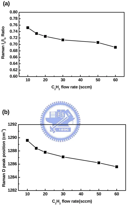
More diamond-like films have generally a lower G peak wavenumber and a lower D peak/G peak intensity ratio, ID/IG ratio, so these two parameters can be used to assess the quality of carbon films. The peak intensities in the Raman spectra were fitted to the sum of two Gaussian line shapes and plotted against the integrated intensity ratio, ID/IG. Figure 3.3 plots the graphs of (a) the Raman ID/IG ratio, and (b) the D peak position of a-C:H films as functions of the C2H2 gas flow rate. Increasing the C2H2 gas flow rate from 10 sccm to 60 sccm decreases the ID/IG intensity ratio from 0.734 to 0.691 and the D peak position from 1288.4 cm-1 to 1285.6 cm-1. The graphs indicate that a higher C2H2 flow rate corresponds to a lower ID/IG ratio and D peak position. With increasing the C2H2 gas flow rate will be decreased the particle energy during growth because of the reduction of the mean free path. Zou et al. found that favors a more porous structure and brings a slow decrease of the density, a decrease of the hardness, and an increase of the hydrogen content, and of the bonding ratio sp3/sp2.[19] Hydrogen doping also greatly affects the structure of an a-C:H films. Raising the C2H2 gas flow rate decreases the ID/IG intensity ratio and shifts the Raman D peak downward, indicating an increase in the sp3/sp2 bond ratio of the a-C:H films.[20,21] According to the model for amorphous carbon proposed by Beeman,[24] the position of the peaks contain information
concerning bond-angle disorder and the bonding in the formed crystallites. The bond-angle disorder with a certain percentage of tetrahedral bonds will shift the D peak and G peak downward. Thus, the a-C:H film possesses diamond-like character as the C2H2 gas flow rate increases.
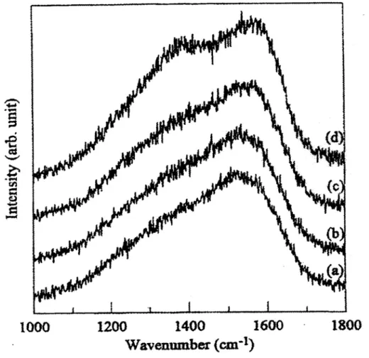
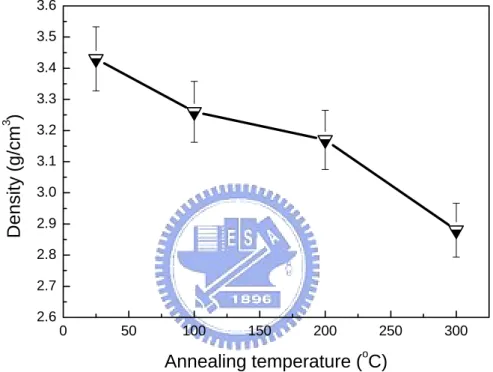
Figure 3.4 shows the Raman spectra of the a-C:H films with different annealing temperatures from 100℃ to 400℃. Figure 3.5 summaries the (a) Raman ID/IG ratio and (b) the D peak position of annealed a-C:H films from Fig. 3.4 as plots versus various annealing temperatures in a vacuum. Increasing the annealing temperature from 100℃ to 400℃ increases the ID/IG intensity ratio from 0.82 to 1.02, but the D peak position herein is unobvious trend. Furthermore, Figure 3.6 presents the variation of the mass density of the film with annealing temperature, as determined by RBS analysis. The figure indicates that the density decreases from 3.44 g/cm3 to 2.89 g/cm3 as the annealing temperature are increased. The mass density (ρ) should indicate the extent to which the films are graphite-like (ρ=2.25 g/cm3) or diamond-like (ρ=3.51 g/cm3). This implies that a-C:H film may contain a small percentage of tetrahedral bonds which are broken upon annealing. Therefore, verified whether the annealed a-C:H film has a progressive micro-structural rearrangement occurs during annealing process. The results are consistent with the model proposed by
Dillon et al.,[21] who predicted a progressive growth in number and/or size of graphitic domains for amorphous carbon films annealed at increasing temperature. Furthermore the intensity ratio ID/IG can be used to get a quantitative estimation of the sp2 cluster size (L). A critical diameter at around 12 Å, which makes ID/IG be a maximum.[22] Below the critical diameter, the Raman measurement on graphite at a different degree of disorder suggested the functional relation
I
D/I
G∝ L (1)
where L is the typical graphite cluster size. When the samples are annealed, the grain size increases, and the relation between relative intensity and grain size can be expressed as [23]
I
D/I
G∝ L
-1 .(2)
As shown in Fig. 3.4(a), the ID/IG intensity ratio increases with annealing temperature, obeying the rule of Eq. (1). The trend of ID/IG intensity ratio decreases with annealing temperature maybe brought by higher annealing temperature that inducing the grain size of sp2 cluster is large enough. During annealing treatment, Friessnegg et al. found that a generation, in the meanwhile, of defects due to hydrogen effusion was observed.[31] Akkerman et al.[32] and Wild and Koidl [33] reported that the released hydrogen atoms and hydrocarbon
radicals produce hydrogen and hydrocarbon molecules in the bulk of the films during annealing; these molecules then diffuse through the carbon network out of the films. If this process also dominates the evolution of hydrogen in the films produced, then the slight increase in thickness is mainly due to the transformation of a diamond-like structure to a graphite-like structure.[34]
The addition of hydrogen to a growing carbon film, such that the generated C2H2 gas reacts with the plasma during film deposition, prevents the nucleation of the graphite phase and stabilizes the tetrahedral bonding, thereby enhancing the diamond-like characteristics of the film.[20,25,26] As the hydrogen content of the films increases, however, the dangling bonds still remains on the surface of the films. The dangling bonds can thus easily react with moisture to form -OH bonds and thus affect the electrical properties. Figure 3.7 plots the leakage current density (J) against applied electric field (E) for a-C:H films annealed at different temperatures. The a-C:H films annealed below 200℃ have a lower leakage current density than the others since the heating removes the absorbed moisture, promotes the movement of hydrogen and activates the electrical defects which compensated unintentional impurities[27] on the film. However, the a-C:H films annealed at 300℃ have a higher leakage current density than the as-deposited films. As previous
describes the effect of overheating on the a-C:H films rearranging their microstructure from a diamond-like one to a graphite-like one, which is a conductive component, thus increasing the leakage current density. The heating also changes the hydrogen distribution and/or content.[28]; transforms the films into graphite-like amorphous carbon films, causing the band-gap to diminish and the carefully nurtured semi-conducting properties to be lost.[29,30] Figure 3.8 shows the dielectric constant (K) of a-C:H films against vacuum annealing temperature and hydrogen plasma treatment period. Figure 3.8(a) shows that vacuum annealing treatment reduces the dielectric constant of the a-C:H films from 3.81 to 3.18 as the annealing temperature increases from 100℃ to 300℃. As previous describes the effusing effects of hydrogen [7] and moisture on a-C:H films as a result of annealing that leaves pores in the insulating film. The decrease of the dielectric constant can be explained as follows: the pores introduced in the film as a result of annealing causes reduction in mass density of the film, shows in Fig. 3.6. Thus, the changes in the character and number of network bonds in the films during annealing lead to an increase in the mean size of the micro-pores.[33] These pores reduce the dielectric constant, since the dielectric constant of air in a pore is close to that of a vacuum. It has a lowest dielectric constant at 3.18 while the a-C:H film
annealed at 300℃.
Hydrogen plasma also affects the electrical properties of the a-C:H films. The as-deposited a-C:H films were treated with hydrogen plasma to reduce their dielectric constant and leakage current, as shown in Fig. 3.8(b) and Fig. 3.9. The variation in the thickness of the films thus treated is hardly visible, but their surfaces become rougher and covered with more pinholes as the period of hydrogen plasma treatment is increased. Horn et al. suggested that under impact of H atoms the hybridization of carbon atoms at a C:H film surface change from sp3 to sp2 character in the temperature range 400 to 700 K.[35] The species of sp2 character is preferentially etched by hydrogen plasma.[36] Thus, the rugged C:H film surface results from hydrogen plasma erosion. Besides, hydrogen ions create dangling bonds by displacement or chemical abstraction of bonded hydrogen in the film in forming hydrogen molecules, which leave the film. The second step concerns the relaxation of these dangling bonds. They can be saturated by free hydrogen atoms or by forming double bonds with neighboring carbon atoms. These processes were established by Horn et al.[35] Thus the surface of the a-C:H film is passivated during hydrogen plasma treatment and the dielectric constant is unobvious change as the plasma period increases. Figure 3.9 shows the leakage current density of
a-C:H films after hydrogen plasma treatment at 250℃ for 1 min, 3 min and 6 min. The leakage current decreases as the period of hydrogen plasma treatment increases. The sp2 content on the surface is etched away during plasma treatment, and the hydrogen radicals help to passivate the surface with respect to air oxidation and annihilate surface dangling bonds. Consequently, the a-C:H films with lower leakage are obtained because the leakage source on the surface is eliminated by the hydrogen-containing plasma. Thus it has a lowest leakage current density of 3×10⁻⁷ A/cm2 with an electric field at 1MV/cm after hydrogen plasma period by 6 minutes. However, the hydrogen plasma interacts with the a-C:H films only in the outermost layer of the film to a thickness of about 40 Å, which is dependent on the ion energy.[37,38] Thus, the hydrogen plasma did not affect the bulk of the a-C:H films. Accordingly, the dielectric constant was not obviously changed as the plasma treatment period increased, but the value was lower than that for the as-deposited films, as shown in Fig. 3.8(b).
The process requires a low-dielectric material or a dielectric material of reduced thickness to reduce the effective dielectric constant in a copper damascene structure. Post-treatment by either annealing or using hydrogen plasma facilitates the reduction of the dielectric constant and leakage current of
a-C:H films. However, after the films were annealed at an elevated temperature (≥ 300 ℃ ), their microstructures were converted from diamond-like to graphite-like and the film density had decreased. The overheated film possessed a higher leakage current density, due to the transition in the microstructure, since the insulation of the graphite-like structure is weaker than that of the diamond-like structure. Otherwise, the properties and the variation in the thickness of those hydrogen-plasma-treated films are hardly visible for a-C:H films, since hydrogen plasma treatment only improves the surface.
3.4 Conclusions
Highly sp3-bonded a-C:H films were deposited using a GIBD system. The films possessed more diamond-like characteristics as the C2H2 flow rate was increased. After the films were annealed at an elevated temperature, their microstructures were changed from diamond-like to graphite-like, and the leakage current density increased. The mass density decreases from 3.44 g/cm3 to 2.89 g/cm3 as annealing temperature is increased, indicating that the annealed a-C:H film has more graphite-like character and thus a higher leakage current density than the as-deposited film, on the other hand, the dielectric constant decreases as the annealing temperature is increased. Hydrogen plasma treatment can significantly improve the electrical characteristics. The variation
of the surface properties of these plasma-treated a-C:H films is barely visible and their electrical properties are greatly enhanced, since hydrogen plasma treatment significantly passivates the surface.
Fig. 3.1 Metal-insulator-semiconductor (MIS) structure.
Al film
p-Si Wafer
Cu film
10 20 30 40 50 60 0.60 0.62 0.64 0.66 0.68 0.70 0.72 0.74 0.76 0.78 0.80
(a)
Ram a n I D /I G Ra ti o C2H2 flow rate (sccm) 10 20 30 40 50 60 1282 1284 1286 1288 1290 1292(b)
R a m a n D p e ak posi ti o n (cm -1 ) C 2H2 flow rate(sccm)Fig. 3.3 Graphs of (a) Raman ID/IG ratio, and (b) D peak position of a-C:H films as functions of C2H2 gas flow rate.
Fig. 3.4 Raman spectra of the a-C:H films with different annealing temperatures, (a) 100℃, (b) 200℃, (c) 300℃, and (d) 400℃.
0 100 200 300 400 0.6 0.7 0.8 0.9 1.0 1.1 1.2
(a)
Ra m a n I D /I G Ra ti o Annealing Temperature (oC) 0 50 100 150 200 250 300 350 400 450 1480 1500 1520 1540 1560 1580 1600 1620 1640(b)
D pe a k pos it ion ( c m -1 ) Annealing temperature (oC)Fig. 3.5 Graphs of (a) Raman ID/IG ratio and (b) D-peak position of a-C:H films with various annealing temperatures in vacuum.
0 50 100 150 200 250 300 2.6 2.7 2.8 2.9 3.0 3.1 3.2 3.3 3.4 3.5 3.6 Density ( g /c m 3 ) Annealing temperature (oC)
Fig. 3.6 Density of a-C:H films for various vacuum annealing temperatures.
0.0 0.5 1.0 1.5 2.0 10-8 10-7 10-6 10-5 10-4 10-3 10-2 300oC 200oC as-deposited 100oC J (A /c m 2 ) E (MV/cm)
Fig. 3.7 J-E curves of a-C:H films with different vacuum annealing temperatures.
0 2 4 6 3.0 3.1 3.2 3.3 3.4 3.5 3.6 3.7 3.8 3.9 4.0
(b)
Hydrogen plasma treatment period (min)0 50 100 150 200 250 300 3.0 3.1 3.2 3.3 3.4 3.5 3.6 3.7 3.8 3.9 4.0
(a)
K Annealing temperature (oC)Fig. 3.8 (a) Dielectric constant (K) of a-C:H films with different vacuum annealing temperatures, and (b) Dielectric constant of a-C:H films with different hydrogen plasma treatment periods.