國
立
交
通
大
學
資訊科學與工程研究所
碩
士
論
文
繪圖處理器中分庫材質快取記憶體之設計
Design of a Banked Texture Cache for Graphic Processing
Unit
研 究 生:康 哲 瑋
指導教授:單 智 君 博士
繪圖處理器中分庫材質快取記憶體之設計
Design of a Banked Texture Cache for Graphic Processing
Unit
研 究 生:康 哲 瑋
Student:Che-Wei Kang
指導教授:單 智 君 博士
Advisor:Dr. Jyh-Jiun Shann
國 立 交 通 大 學
資 訊 科 學 與 工 程 研 究 所
碩 士 論 文
A Thesis
Submitted to Institute of Computer Science and Engineering
College of Computer Science
National Chiao Tung University
in Partial Fulfillment of the Requirements
for the Degree of
Master
In
Computer Science
Auguest 2007
Hsinchu, Taiwan, Republic of China
繪圖處理器中分庫材質快取記憶體之設計
學生:康哲瑋 指導教授:單智君 博士 國立交通大學資訊科學與工程研究所 碩士班摘 要
在現今繪圖處理器中,材質過濾器演算法需要多個紋素(材質上的最小單位)去混色 出最後顯示在螢幕的顏色。由於這些紋素在材質快取記憶體可能散在數個區段中或是分 散在同一個區段中不連續的位子。這樣的情形使得完成一次過材質過濾可能要多次存取 材質快取記憶體,讓整體處理時間變長。然而多次的快取記憶體存取間接也造成動態電 力的消耗提高。在此篇論文我們提出了分庫的材質快取記憶體設計,利用雙向性過濾演 算法以及材質擺放的特性下去設計。我們提出兩種資料庫的設計,分別是插敘資料庫和 連續資料庫。此外我們也設計分庫標籤,以降低每次存取需要多筆標籤比對的代價。我 們的設計可以讓做雙向性處理時,只需要去材質快取記憶體存取一次即可拿到所需的紋 素。跟寬的匯流排設計比較,在畫面解析度為1280×1024下,分庫的材質快取記憶體減 少大約50%的快取記憶體存取次數。由於存取的次數減少,兩種分庫設計分別減少大約 44%以50%的材質快取記憶體的動態電力消耗。Design of a Banked Texture Cache for Graphic Processing
Unit
Student:Che-Wei Kang Advisor:Dr. Jyh-Jiun Shann
Institute of Computer Science and Engineering National Chiao-Tung University
Abstract
In modern Graphic Processing Unit (GPU), texture filter needs several texels (element of
texture) to compute the final color in screen. The requested texels of texture filtering may be
in different cache lines or discontinuous position of a cache line. This makes finishing one
filtering may have to access texture multiple times. Multiple cache access causes the process
time longer. However, multiple cache access also causes the dissipation of access power high.
At this thesis, we proposed a banked texture cache which is according to bilinear filtering and
texture placement. We design two kinds of data bank. The two kinds of data bank are
interleaved data bank and continuous data bank. And we also design tag bank to reduce the
cost of multiple tag comparison. The banked texture cache can fetch the requested texels of
bilinear filtering in one cache access. Compare with wide bus design, banked texture cache
can reduce 50% of cache access times. The access energy of two kinds of texture cache are
III
誌 謝
首先感謝我的指導老師 單智君教授,在老師的諄諄教誨、辛勤指導與勉勵下,我 得以順利完成此論文,並且順利通過畢業口試。同時感謝我的另一位參與計劃老師兼口 試委員 鍾崇斌教授以及口試委員 陳青文教授以及 邱日清教授,由於他們的指導與建 議,讓這篇論文更加完整和確實。 此外,感謝指導我的惠親學姊,學姊在論文上給了我很多寶貴的意見。還有喬偉豪 學長、吳奕緯學長以及各位實驗室的大家,經常在各種問題上給予我不同的建議。還有 同樣今年一起畢業的辰瑋、立傑、慧榛、志遠、易叡。感謝實驗室的大家,謝謝你們陪 我度過充實又快樂的兩年研究生活。 在此也要感謝我的女朋友,雅婷。在忙碌的時候,我總是沒有時間陪伴她。但是妳 總是在我心情不好時一直鼓勵我,讓我有動力繼續努力。很感謝有這麼一位妳陪著我, 跟妳在一起真的很幸福。 最後感謝我的家人,謝謝你們在背後全心全意地支持我,讓我在這研究的路上走得 更順利,進而能無後顧之憂的學習,讓我追求自己的理想。 謹向所有支持我、勉勵我的師長與親友,奉上最誠摯的祝福,謝謝你們。康哲瑋
2007.08.27
Table of Contents
摘 要 ...I Abstract... II 誌 謝 ... III Table of Contents...IV List of Figures...VI List of Tables ... VIIIChapter 1 Introduction... - 1 -
1.1 GPU and Programmable Graphics Render Pipeline... - 1 -
1.1.1 Vertex Processing ... - 3 -
1.1.2 Triangle Setup & Rasterization... - 3 -
1.1.3 Pixel Processing... - 4 -
1.1.4 Depth Processing ... - 4 -
1.2 Texture Mapping and Texture Filtering ... - 4 -
1.2.1 Texture Mapping... - 5 - 1.2.2 Texture Filtering ... - 6 - 1.3 Texture Unit ... - 9 - 1.4 Motivation ... - 9 - 1.5 Objective... - 10 - 1.6 Thesis Origination ... - 10 - Chapter 2 Background ... - 11 - 2.1 Texture Placement ... - 11 -
2.1.1 Texture Placement Method: 4D ... - 11 -
2.1.2 Texture Placement Method: 6D ... - 13 -
2.1.3 Texture Placement Method: Recursive Z (RZ)... - 14 -
Chapter 3 Design ... - 17 -
3.1 System Overview... - 17 -
3.2 Data Bank Design v1: Continuous Data Bank ... - 18 -
3.1.1 Address Mapping in Cache... - 19 -
3.1.2 Address Control ... - 21 -
3.1.3 Word Select... - 23 -
3.1.4 Discussion of Continuous Data Bank... - 24 -
3.2 Data Bank Design v2 (Interleaved Data Bank) ... - 26 -
3.2.1 Address Mapping in Cache... - 27 -
V
3.3 Banked Tag ... - 32 -
3.3.1 Tag Control ... - 34 -
3.3.2 Tag Compare... - 35 -
3.3.3 Discussion of Banked Tag ... - 35 -
3.4 Cache Miss Replacement ... - 36 -
Chapter 4 Experiment Result... - 38 -
4.1 Simulation Environment... - 38 -
4.1.1 Software Simulation Environment ... - 38 -
4.1.2 Hardware Simulation Environment ... - 38 -
4.2 Software Simulation Result ... - 39 -
4.2.1 Cache Access Count ... - 39 -
4.2.2 Total Access Energy ... - 43 -
4.3 Hardware Simulation Result... - 45 -
4.3.1 Timing Comparison ... - 45 -
4.3.2 Area Comparison ... - 48 -
Chapter 5 Discussion and Conclusion ... - 51 -
5.1 Discussion... - 51 -
5.2 Conclusion ... - 53 -
Reference ... - 55 -
List of Figures
Fig. 1-1 Programmable graphics render pipeline ... - 2 -
Fig. 1-2 Horizontal scan line into primitive ... - 3 -
Fig. 1-3 A texture, its width and height are all eight ... - 5 -
Fig. 1-4 Concept of texture mapping... - 6 -
Fig. 1-5 A texture mapping example [6]... - 6 -
Fig. 1-6 Concept of texture filtering and mip-map... - 7 -
Fig. 1-7 Concept of anisotropic filtering ... - 8 -
Fig. 1-8 Texture Unit ... - 9 -
Fig. 2-1 A 4D placement example with 4×4 tile size... - 12 -
Fig. 2-2 Address translation equation of 4D placement ... - 12 -
Fig. 2-3 6D placement example with 4×4 1st level tile and 8×8 2nd level tile ... - 13 -
Fig. 2-4 Address translation equation of 6D placement ... - 14 -
Fig. 2-5 RZ placement example ... - 15 -
Fig. 2-6 Address translation equation of RZ placement ... - 16 -
Fig. 3-1 Origination of the texture cache: (a) original texture cache (b) banked texture cache ... - 18 -
Fig. 3-2 Data bank design v1: Continuous data bank... - 19 -
Fig. 3-3 data bank id field in address... - 19 -
Fig. 3-4 address mapping in data bank ... - 20 -
Fig. 3-5 Example of address mapping in data bank: (a) Texel mapped address with RZ placement (b) address mapping in data bank... - 21 -
Fig. 3-6 Address control: Ai is the address from ATi and Bi is the data bank id of Ai... - 22 -
Fig. 3-7 Circuit of priority encoder ... - 22 -
Fig. 3-8 Word select... - 24 -
Fig. 3-9 Si and MUXi in address with tile size 2×2 ... - 24 -
Fig. 3-10 An conflict situation in continuous data bank... - 25 -
Fig. 3-11 Data bank design v2: interleaved data bank... - 27 -
Fig. 3-12 texel mapping in data bank ... - 27 -
Fig. 3-13 Data bank id and offset in data bank field in address with 2×2 tile size... - 28 -
Fig. 3-14 Texel mapping in interleaved data bank which tile size is 2×2 and cache line size is 64 byte... - 28 -
Fig. 3-15 Address mapping in interleaved data bank, which tile size is 2×2 and cache line size is 64 bytes... - 29 -
Fig. 3-16 Data bank id and offset in data bank field in address with 4×4 tile size... - 29 -
VII
Fig. 3-18 Address mapping in interleaved data bank, which tile size is 4×4 and cache line
size is 64 bytes... - 30 -
Fig. 3-19 Cases of switching address to corresponded data bank. ... - 31 -
Fig. 3-20 Address control in data bank design v2 ... - 32 -
Fig. 3-21 Proposed banked tag design... - 33 -
Fig. 3-22 Tag index field and tag bank id in address... - 33 -
Fig. 3-23 Tag control ... - 34 -
Fig. 3-24 Circuit of modified tag comparison ... - 35 -
Fig. 3-25 A conflict situation of banked tag ... - 36 -
Fig. 3-26 Cache miss replacement example: (a) Cache miss happen (b) Replace all the same line of each data bank... - 37 -
Fig. 4-1 Access count of each design: (a) traditional design (b) wide bus design (c) multi-port, banked designs ... - 41 -
Fig. 4-2 per access energy of each line size with 16KB texture cache... - 41 -
Fig. 4-3 Cache access count comparison with traditional as baseline... - 42 -
Fig. 4-4 Cache access count comparison with wide bus as baseline... - 43 -
Fig. 4-5 Energy of per access ... - 44 -
Fig. 4-6 Total cache access energy of one frame... - 45 -
Fig. 4-7 Delay of data access time... - 47 -
Fig. 4-8 Delay of tag access... - 47 -
Fig. 4-9 Delay of cache access ... - 48 -
Fig. 4-10 Area comparison of each design ... - 49 -
Fig. 4-11 Percentage of extra circuit of banked texture cache ... - 50 -
Fig. 5-1 block of each cache design: (a) One data array, output is 128 bits (b) Interleaved data bank with four tag arrays, output of each bank is 32bits (c) Interleaved data bank with share tag, output of each bank is 32bits (d) Interleaved data bank with banked tag, output of each bank is 32 bits (e) Continuous data bank with banked tag, output of each bank is 128 bits ... - 52 -
List of Tables
Table 1-1 Input, output and operation of each stage... - 2 -
Table 1-2 Comparison of bilinear, trilinear, and anisotropic filtering algorithms ... - 8 -
Table 3-1 Truth table of priority encoder... - 23 -
Table 4-1 Cache configuration applied in our designs ... - 42 -
Table 4-2 bank number, access port of each design ... - 46 -
Table 4-3 clock frequency of GPU which its process 0.13 um ... - 48 -
Chapter 1 Introduction
1.1 GPU and Programmable Graphics
Render Pipeline
Graphic processing unit (GPU) is a growing of field of application specific
processor. It targets on graphics rendering, which display the two-dimensional (2D)
viewing of three-dimensional (3D) space. Complexity of modern GPU becomes more
complex due to users’ increasing demands for 3D scene realism improvement [1].
Programmable graphics pipeline is the most popular solution for the requirements
of both performance and flexibility in computer graphics nowadays. With the rapidly
development of computer graphics, such as 3D games, virtual realities and digital
lives, the requirements of computer graphics in effects and performance become
higher [15]. To meet all kinds of users’ requirements, programmable graphics pipeline
have been introduced into graphics hardware and many complicated function units
have been put in. Different from fixed-functionality (non-programmable) graphics
pipeline, programmable graphics pipeline has new graphics processing units: vertex
shader unit and pixel shader unit. These two new processing units give graphics
pipeline the flexibility to deal with all kinds of computation requirements while
retaining the capability of complicated computation.
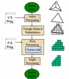
Fig. 1-1 is the programmable graphics render pipeline, we discuss the render
pipeline in several parts, which are vertex processing, rasterization, pixel processing
Fig. 1-1 Programmable graphics render pipeline
Table 1-1 shows the input, output and operations of each stage to give a concept of
the graphics pipeline. Then we introduce the detail operations of each stage in the
follow sub-sections.
Stage Input Output Operation
Vertex Processing Vertices with 3D coordinates Vertices positioned in the 2D scene Transforms 3D vertex in world space to 2D vertex on scene Triangle Setup &
Rasterization
Triangles assembled by vertices
Fragments Interpolates each
triangle into numbers of fragments
Pixel Processing Fragments Pixel with final color
Colors each fragment according to its information Depth Processing Pixel with final color
value
Image composed of ‘finalized’ pixel
Uses frame buffer storing pixels which will be showed in screen
1.1.1 Vertex Processing
Vertex processing is supported by vertex shader in GPU [4]. Vertex shader performs
mathematics operations on the vertex data for objects by the vertex shader programs.
Vertex data are the 3D coordinate values (which are x, y and z) for the vertex and an
object consists of three vertexes. Vertex shader does several transformations and
normalizations, which are model-view transformation, projection transformation,
Clipping, perspective division and viewport mapping. After the transformations and
normalizations, the 3D based objects will be transformed into normalized 2D based
objects on screen which all the coordinate values are in the interval 0 and 1. Then
vertex processing sends the normalized 2D coordinate values to rasterization which
will be introduced at next section.
1.1.2 Triangle Setup & Rasterization
Rasterization receives the data from vertex processing, then produces the fragments
which are in the primitive. It uses horizontal scan line onto the primitive to produce
fragments, which is showed below Fig. 1-2.
1.1.3 Pixel Processing
Pixel processing is supported by pixel shader. Pixel shader receives fragments from
rasterization stage and does computations for the fragments. Each fragment will be
colored according to the pixel shader code, including texture mapping which we will
introduce in section 1.2. After pixel processing, the fragments with final color will be
sent to depth processing.
1.1.4 Depth Processing
Using frame buffer to store the pixel color which will be display on the screen. In
this stage, z value of every pixel is compared with z value which has the same screen
address (means has the same x, y values) of Z-Buffer. Z-Buffer is a buffer of
screen-size using to store the nearest z value of every pixel [5]. If z value of the pixel
is smaller than the value of the Z-Buffer, Z-Buffer is updated by the z value and frame
buffer is updated by the new color. After depth processing, screen display the colors
which are stored in frame buffer.
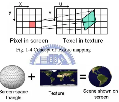
1.2 Texture Mapping and Texture Filtering
At this section, we will introduce an important technique in GPU which is calledtexture mapping. We also introduce two techniques used in texture mapping in the
1.2.1 Texture Mapping
Before introducing texture mapping, we introduce texture at first. Texture is a 2D
bit-map object and its width and height are powers of two. The max size of texture
supported in modern GPU is 4096. Element of texture is called texel, it is consist of
four components which are red (R), green (G), blue (B), and alpha (A). R, G, and B
are the value of color. A is the value of transparency. Each component is 1 byte, is
means that each texel is four bytes. An example is shown in Fig. 1-3. As Fig. 1-3
shows, width and height of the texture are eight. It means that size of the texture is 4×
8×8=256 bytes.
Fig. 1-3 A texture, its width and height are all eight
Texture mapping is a relatively efficient means to reduce computations for realistic
scenes without the tedium of modeling and rendering every 3D detail of a surface [2,
3]. It is a process in which a texture is applied to an object in the 3D world, as shown
in Fig. 1-4. X and y are pixel coordinates. U and v are texture coordinates.
The number of required triangles is increased and thus the number of calculations is
increased due to realize realistic images or a very complex image. The number of
polygons should be reduced because the computing power of the given system is not
of scene complexity is introduced but in some cases this degradation is not tolerable.
Hence, to have more realistic images with less geometric data, texture mapping has
been used commonly in 3D computer graphics.
Fig. 1-5 shows an example that a texture is mapped onto an object. The object (a
ball) which a texture (a world map) is mapped onto the object shown on screen is a
globe.
Fig. 1-4 Concept of texture mapping
Fig. 1-5 A texture mapping example [6]
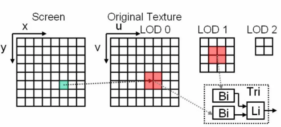
1.2.2 Texture Filtering
Due to the absence of no one-to-one mapping between texels and pixels, an
interpolation calculation is necessary for high quality mapping. Higher quality
requires computation intensive interpolation to generate a final pixel value from many
texel values.
Commonly used texture filtering algorithms in current 3D games are bilinear
tradeoff between operation complexity and image quality among various texture
filtering algorithms. Both trilinear and anisotropic support the mip-map technique.
Mip-map is a technique to reduce the artifacts which arise from the use of a single
bitmap image while the level of detail of an object decreases with an increase in the
distance. It is made by an original-size texture with level-of-detail 0 (LOD 0), then
iteratively resample it to make a quarter-sized texture with LOD i (i>0). The number
of LOD depends on application designer. In Fig. 1-6, there are three LODs for
mip-map. The original size of texture (LOD 0) is 8×8, the size of LOD 1 is 4×4, and
the size of LOD 2 is 2×2.
Fig. 1-6 Concept of texture filtering and mip-map
The final value of filtering is weighted average of several color values of texels.
The value of bilinear is weighted of four texels that are closest to the center of the
pixel being textured. Trilinear filtering is to choose two adjacent mip-maps which are
most closely match the size of the pixel being textured. First, use bilinear filter to
produce a texture value from each mip-map. Second, do linear average of theses two
results from bilinear filtering. An example is in Fig. 1-5, two mip-maps are LOD 0
and LOD 1. The final color value is weighted average of the values which are after
If we need to do texture mapping for a plane which is at an oblique angle to the
camera, traditional filters (bilinear/trilinear) don’t have sufficient horizontal resolution
and extraneous vertical resolution. Anisotropic is a method of enhancing the image
quality of textures on surfaces that are far away and steeply angled with respect to the
camera. The final color value of n:1 anisotropic is an average of the values of n
trilinears results. The value n is called anisotropic ratio, the ratio of horizontal
direction to vertical direction, is defined by game designer. The value may be 2, 4, 8,
or 16. We use n=2 as example and shown in Fig. 1-7. Table 1-2 is comparison of three
types filtering algorithms.
Fig. 1-7 Concept of anisotropic filtering
Filtering Type # of Mip-map # of Texel / Mip-map # of Texel
Bi 1 4 4
Tri 2 4 8
n:1 Ani, n=2,4,8,16 2 4n 8n
1.3 Texture Unit
Texture unit supports texture mapping operation in GPU. Texture unit is composed
of an address translation, texture cache, and texture filter, as shown in Fig. 1-8.
Process of texture unit is that texture unit receives texture coordinate (u, v). Then
address translation translates the texture coordinate (u, v) of texel into real address,
then sends the address to texture cache to fetch texel. This action may active several
times. After all the requested texels are sent to texture filter, texture filter will compute
the final color value according to the filter type and weight then sends the color value
to pixel shader.
Fig. 1-8 Texture Unit
1.4 Motivation
The texture filtering algorithms in modern GPU always need several texels. In
traditional single port texture cache, it may need several times of cache access. This is
wasteful of processing time and access power.
The power dissipation of cache on modern processor is an important part [7]. For
example, power dissipation of on-chip D-cache in the StrongARM110 is 16% of its
the requested in one cache access. But the overhead of multi-port cache is too heavily.
1.5 Objective
Design a banked texture cache which is according to bilinear filtering. Other
complex filtering algorithms can be seen as several times of bilinear filtering.
Trilinear filtering can be seen as two times of bilinear filtering and N:1 anisopostic
filtering can be seen as 2N times of bilinear filtering. The banked texture can fetch the
requested texels of bilinear filtering in one cache access if there is no cache miss. The
performance of our banked texture cache is the same as multi-port texture cache but
the cost is lower than multi-port texture cache.
We use the characteristic of bilinear filtering which needs 2×2 texels to separate the
original texture cache into four banks. Cache line size of each bank is quarter of
original cache line size.
1.6 Thesis Origination
The origination of follow sections in this thesis is: Chapter 2 introduces background
of texture placement and a related work. Chapter 3 introduces our banked design,
including two kinds of data bank design and banked tag design. Experiment results
Chapter 2 Background
In this chapter, we will introduce the texture placement methods which our
banked texture cache rests on. The texture placements which we will introduce are 4D
placement, 6D placement, and recursive Z (RZ) placement. We will introduce how
they map the texture in memory and the address translation equations.
2.1 Texture Placement
Texture placement is to map the 2D based texture in texture memory (can see as
map 2D object on 1D). The representation of texture maps in memory is important to
the cache behavior because it effects where texture data is placed in the cache [9].
Placement also effects complexity of address translation logic. Texture placement can
be separated into two kinds which are non-tile based and tile based. Non-tile based
placement method is linear and tile based placement methods are 4D, 6D and RZ.
At this section, we will introduce the tile based placement methods which we use
for our banked texture cache. These placements methods are 4D, 6D [9], and
Recursive Z (RZ) [10].
2.1.1 Texture Placement Method: 4D
4D placement is a tile based placement, texels that are within a square region of 2D
image are order consecutively in memory. The tile sizes for width and height are equal
and are powers of two. An illustration of 4D placement is shown in Fig. 2-1, which
the order of texel. The right part is texels (tiles) placement order in texture memory.
Fig. 2-1 A 4D placement example with 4×4 tile size
The address translation equation is shown in Fig. 2-2. Its concept has two steps.
First step is to calculate the tile start address which the requested texel is in it. Second
is to calculate the texel address by adding offset in the tile to tile start address
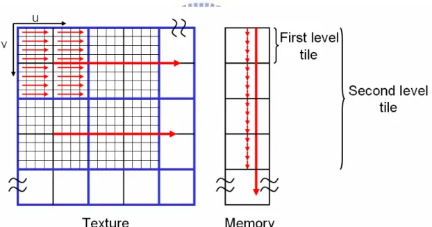
2.1.2 Texture Placement Method: 6D
6D placement is also a tile based placement which is like 4D placement. The
difference between 4D placement and 6D placement is that 6D placement has
two-level tile. The limits of two-level tile width and height are the same as tile width
and height of 4D placement. But the second level tile size has to be bigger than first
level tile size. An illustration of 6D placement with first level tile size is 8×8 and
second level tile size is 4×4 is shown in Fig. 2-3. The left part is the 2D texture, and
the red line means the order of texel in memory. The right part is the order of texels in
the memory.
Fig. 2-3 6D placement example with 4×4 1st level tile and 8×8 2nd level tile
The address translation of 6D placement is like 4D placement. The difference
between these two placements is that 6D placement has two level tiles, so 6D
placement has to calculate tile start address two times. First step is to calculate the
second level tile start address which the requested texel is in. Second step is to
offset to second level tile start address. At last, calculate the offset by adding the intra
second level tile offset to the second level tile start address. The equation is shown in
Fig. 2-4.
Fig. 2-4 Address translation equation of 6D placement
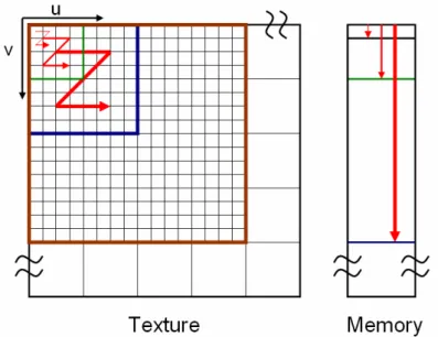
2.1.3 Texture Placement Method: Recursive Z (RZ)
Recursive Z placement can be seen as multi-level tile placement. Each first level
tile has four texels. Each second level tile has four first level tiles (16 texels). From
this rule, we can know that each third level tile has four second level tiles (64 texels)
and so on.
Fig. 2-5 shows an illustration of RZ placement. The first level tile is shown as the
smallest “Z” in Fig. 2-5. The second level tile is shown as middle “Z” in Fig. 2-5. The
third level tile is shown as the biggest “Z” in Fig. 2-5. Using this rule can map the
Fig. 2-5 RZ placement example
The address translation of RZ is shown in Fig. 2-6. The concept of RZ placement is
bit interleaved by texture coordinate (u, v). As Fig. 2-6 shows, there are three cases of
texture, which are width is equal to height (case 1), width is smaller than height (case
2), and width is bigger than height (case 3). In case 1, assume width and height of
texture have n valid bits (Ex: the valid bits of 128 are 7). The valid bits of offset are
2n bits which are made by the bits of u direction and v direction interleaved. The
interleaved method is that u direction offers a bit then v direction offers a bit and
repeats until the u and v direction valid bits are use over. Case 2 and case 3 are like
case 1, but the difference is that the bits interleaved until the small value bit length
then the other bits in offset are offer by the leaved bits of big value. If the bits length
Chapter 3 Design
In this chapter, we will introduce our design of banked texture cache. We will
introduce two kinds of design which are interleaved data bank and continuous data
bank. Then, we will introduce the banked tag which is to reduce to access port in tag.
3.1 System Overview
At this section, we introduce the differences between traditional texture cache and
banked texture cache. We discuss them in two parts, which are data array and tag array.
In data array, our design is to separate data array into four data banks (DB0~DB3).
The cache line size of each data bank is quarter of original cache line size and number
of lines is the same as original texture cache. In tag array, banked texture cache
separates the tag array into four tag banks (TB0~TB3). The number of line of each tag
bank is quarter of original tag array.
We will introduce two kinds of data bank designs at section 3.2 and section 3.3. Tag
bank design will be introduced in section 3.4
Fig. 3-1(b)
Fig. 3-1 Origination of the texture cache: (a) original texture cache (b) banked texture cache
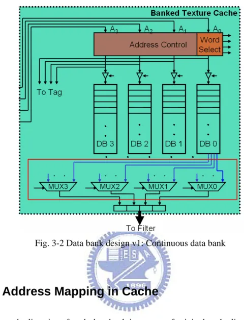
3.2 Data Bank Design v1: Continuous Data
Bank
The concept of reducing access power in continuous data bank is by less data bank
access. The proposed data bank design v1 is shown in Fig. 3-2. From Fig. 3-2 we can
find that the requested texels may be in one, two or four data banks. To get the
requested texels in all cases, the column select is outside each data bank and the
inputs of each column select is interleaved from each data bank.
The extra circuit has two parts which are address control and word select. Address
control is to send correct addresses to correct data bank and gate needless access
which will be introduced in section 3.2.2. Word select is to produce the select signal
Fig. 3-2 Data bank design v1: Continuous data bank
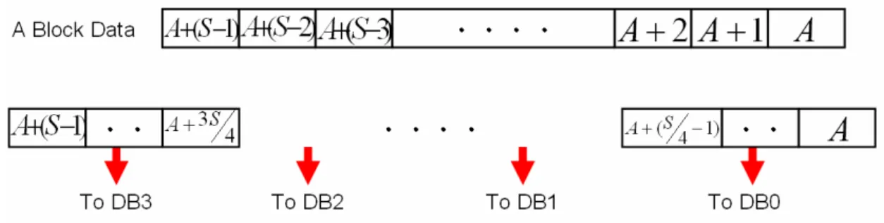
3.1.1 Address Mapping in Cache
Because the line size of each data bank is quarter of original cache line size, so the
data bank id field of address is the highest two bits of line offset field. The data bank
id field in address is shown in Fig. 3-3. The lowest two bits of address are word offset.
Fig. 3-3 data bank id field in address
From Fig. 3-3, we find that texels in data bank is separate a line data into four parts
S
is the block start address and is the cache lines size in texel.
Fig. 3-4 address mapping in data bank
Fig. 3-5 is an example of address mapping in continuous data bank. The texture
placement method is RZ placement and cache line size is 64 bytes (16 texels). Fig.
3-5(a) is the texel mapped address with RZ placement. The number above in each
texel is the address and the number below is the line offset binary code of each
address. In the line offset binary code, the italic and boldface is the data bank id. Fig.
3-5 (b) is the address mapping in data bank. Use the rule shown in Fig. 3-4, texels
with address 0, 1, 2, 3 have the same data bank id are placed the same data bank
(DB0), and texels with address 4, 5, 6. 7 are placed in the same data bank (DB1) and
so on.
Fig. 3-5(b)
Fig. 3-5 Example of address mapping in data bank: (a) Texel mapped address with RZ placement (b) address mapping in data bank
3.1.2 Address Control
Because in continuous data bank, we find that the requested texels may be in 1, 2,
or 4 data banks. To send addresses to data bank in all cases is the function of address
control. Address control is to check the addresses and send the only one address to its
corresponded data bank. We use four comparators to compare the data bank field of
the four addresses.
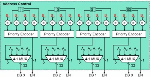
Address control consists of comparators, priority encoders and multiplexers. The
four comparators send the results of comparison to a priority encoder. The priority
produces an address select signal and a data bank enable signal. The select signal is
sent to multiplexer for selecting the address to the data bank. The address control
circuit is shown in Fig. 3-6. The input of each comparator Bi is the data bank id of the
address which is from ATi. And the inputs of each multiplexer are the addresses from
Fig. 3-6 Address control: Ai is the address from ATi and Bi is the data bank id of Ai
We use the control of DB0 as example. The data bank field of each address is
compared with binary signal “00”. If the data bank field matches the binary signal, the
result is “1” otherwise is “0”. The results of the comparators are as inputs of priority
encoder, the priority encoder accords to the priority truth table to produce a select
signal to multiplexer. The data bank enable signal is also produced from priority
encoder. If one of the inputs is not “0”, the bank enable signal is “1”. It means that
there is address will be sent to DB0. Otherwise, all inputs are “0” means that no
address will be sent to DB0.
The priority encoder circuit is shown in Fig. 3-7, and Table 3-1 is the truth table of
the priority encoder.
X3 X2 X1 X0 Y1 Y0 EN 1 X X X 1 1 1 0 1 X X 1 0 1 0 0 1 X 0 1 1 0 0 0 1 0 0 1 0 0 0 0 X X 0
Table 3-1 Truth table of priority encoder
3.1.3 Word Select
Before introducing word select, we introduce how texels in cache line to be inputs
of multiplexers first. In our design, we want to design that the requested texels is from
each multiplexer. So we let the cache data be the inputs of multiplexers interleaved.
Assume that texture placement tile size is NxN and texel address is A . Texel
should be sent to the multiplexer with number A[log2(N)+3][3], and the position in
the multiplexer is the remain bits of line offset field. Use this rule can let the requested
2×2 texels be in each multiplexer individually.
The function of word select is to produce select signals for outside data bank
multiplexers. The signals are the positions of the requested texels in each multiplexer.
The inputs of word select are line offset fields of texel addresses. Then separate each
line offset field into two parts which are select signal for outside data bank
multiplexer and select signal . These two fields depend on tile size,
is and is remain bits of line offset field. Use
as the select signal and as the inputs of multiplexers. The reason is that texels
i
S MUXi i
MUX Ai[log2(N)+3][3] Si MUXi
i
placed in cache are continuous, but we design the outside bank column select which
its input are interleaved. So, the and are like the data bank id and offset
in bank field in interleaved data bank design respectively. The and for
other tile size are also mapped to the data bank field and offset field in interleaved
data bank. The word select circuit is shown in Fig. 3-8. There are four multiplexers
and each output of the multiplexer is the select signal for outside data bank cache
column select.
i
MUX Si
i
MUX Si
Fig. 3-8 Word select
Use tile size is 2×2 as example. Use the cache data to outside data bank rule,
is ( ] ) and other bits of line offset field is . Fig,
3-9 shows field and field in address with tile size 2×2.
i
MUX Ai[log2(2)+3][3] Ai[4][3 Si
i
MUX Si
Fig. 3-9 Si and MUXi in address with tile size 2×2
3.1.4 Discussion of Continuous Data Bank
parameters will happen the requested texels are in same data bank but in different
cache lines. A conflict example is shown in Fig. 3-10. Tile size of texture placement is
2×2 and cache line size is 64 byte. If the requested texels addresses of bilinear are 2, 3,
16, and 17, conflict happens. The four addresses are all mapped in DB0 but the texels
with address 2, 3 are in a cache line, texels with address 16, 17 are in another cache
line.
Conflict situations happen in the wrong texture placement tile size and cache line
size parameters. Especially in large cache line size, conflict situation may happen in
each texture placement tile size.
Fig. 3-10 An conflict situation in continuous data bank
Address control is complex due to several access situations. The requested texels of
bilinear filtering may be in one, two, or four data banks. Address control is designed
to control each situation, so the circuit is complex.
Another problem is that we design the cache data (texels) are inputs of outside data
bank multiplexers interleaved, output bit of each data bank is equal to the line size of
data bank. It means that the dynamic energy consumption of each data bank is high. If
the requested texels are in two or four data banks, the dynamic energy of per access is
3.2 Data Bank Design v2 (Interleaved Data
Bank)
In data bank design v1, there are some access situation cases. These access cases
make the address control complex. And the output bit of each data bank is wide. In
data bank design v2, we want to design a simpler data bank and the address control is
also simpler.
Basic idea of interleaved data bank is that the requested texels of bilinear filtering
are in different data banks. Output bit of each data bank is one texels. This concept of
interleaved data bank is that from [11], Igehy proposed a texture data organization
which use 6D placement. We follow this concept to design our interleaved data bank.
The proposed data bank v2 is shown Fig. 3-11. The extra circuit called address control
is to switch the texel addresses to the correct corresponded data bank, we will
introduce it at section 3.2.2.
Fig. 3-12shows that the texels are interleaved mapped in data bank. The left part is
the texture and number is the coordinate of texels. The right part is the texels mapped
data bank number. We can find that in each 2×2 tile, texels in the tile are from
different data banks, so that one bilinear filtering can fetch the four texels from four
data banks in one cache access. The difficulty of interleaved data bank is that how we
map the texels in data bank interleaved by addresses. To do that, we analyze each
texture placement methods introduced in chapter 2 and to find the mapping method to
Fig. 3-11 Data bank design v2: interleaved data bank
Fig. 3-12 texel mapping in data bank
3.2.1 Address Mapping in Cache
For mapping address to cache, the mapping rule is like the rule introduced in data
bank design v1. Consider the texture placement tile size which is , the texel
with address
NxN
A is in data bank A[log2(N)+3][3] and position in data bank is the remain bits of line offset.
First, we use texture placement tile size 2×2 (Ex: 4D_2×2, 6D_N×N_2×2, RZ) as
example. Texel which its address is A , the data bank id is
( ) and offset in data bank is the remainder bits of line offset. The data bank id
and offset in data bank field in texel address are shown in Fig. 3-13
] 3 ][ 3 ) 2 ( [log2 + A ] 3 ][ 4 [ A
Fig. 3-13 Data bank id and offset in data bank field in address with 2×2 tile size
Use this rule to map a texture in cache. An example is shown in Fig. 3-14, texture
placement method is RZ and cache line size is 64 bytes. The number above is the
address of texel and number below is the binary code of the address. We find that use
the boldface and italic numbers of binary code as data bank id, each texel in 2×2 tile
can be placed in different data banks.
Fig. 3-14 Texel mapping in interleaved data bank which tile size is 2×2 and cache line size is 64 byte
Fig. 3-15 is the address mapping in cache which is following the example shown in
Fig. 3-14. Texels which addresses are 0, 4, 8, and 12 are placed in the same data bank
9, and 13 are placed in the same data bank (DB1) because they have the same data
bank id (01), so are other texels.
Fig. 3-15 Address mapping in interleaved data bank, which tile size is 2×2 and cache line size is 64 bytes
We use tile size is 4×4 as another example. From the mapping rule, texel with
address A is at data bank A[log2(4)+3][3] ( ) and the position in data bank is the remainder bits of line offset. Fig. 3-16 shows the data bank id and position in
data bank field in address which texture placement tile size is 4×4. ] 3 ][ 5 [ A
Fig. 3-16 Data bank id and offset in data bank field in address with 4×4 tile size
The concept is that u direction of texture coordinate place four texels then v
direction of texture coordinate place one texel. It can be seen as that the u direction
offers two bits then v direction offers one bit. So, we can use this concept to place
each 2×2 tile of texture in data bank interleaved which texture placement tile size is 4×
4. The data bank id is the boldface and italic number of the binary code of address in
Fig. 3-17 Texel mapping in interleaved data bank with 4×4 tile size
Fig. 3-18 shows an example of address mapping in data bank which is following
the example shown in Fig. 3-17. Assume cache line size is 64 bytes (16 texels). Texels
with address is 0, 2, 8, and 10 are placed in the same data bank (DB0). The texels with
address 1, 3, 9, and 11 are placed in the same data bank (DB1) and so on. From Fig.
3-18 we can find that the requested texels are in different data banks for each 2×2
texels.
Fig. 3-18 Address mapping in interleaved data bank, which tile size is 4×4 and cache line size is 64 bytes
Use the rule to find other tile size interleaved mapping method. Tile size is 8×8 uses
third and fifth bits of address to be data bank id and so on.
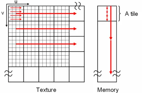
The constraint of the interleaved data bank is that the cache line size has to be the
smallest tile size at least. If the cache line size is small than tile size, the data in a line
are not continuous. For example, if cache line size for tile size is 4×4 is 16 bytes, it
address 2, 3, 6, 7. At this situation, if cache is missed, memory may have to transmit
several times. This makes miss plenty be worse.
3.2.2 Address Control
The function of address control in data bank design v2 is to switch the address to
corresponded data bank. It receives addresses from the address translation array and
then switches the addresses to the corresponded data bank. There are four cases which
are address mapping data bank of bilinear filtering, shown in Fig. 3-19. First, see the
above part, four texels masked by square are the requested texels of bilinear filtering.
The below part is address control how to switch the addresses to the corresponded
data bank.
Fig. 3-19 Cases of switching address to corresponded data bank.
By analysis of the four cases, we find the situation that the address from ATi is sent
to DBj (i and j are 0~3), and the address from ATj is sent to DBi. It can be seen as two
of the four addresses change its address. So we use four 4-1 multiplexer to implement
corresponded AT. The implementation circuit of address control is shown in Fig. 3-20.
Fig. 3-20 Address control in data bank design v2
3.2.3 Discussion of Interleaved Data Bank
The effect of accessing four data banks in one cache access is waste of dynamic
power. But output bit of each data bank is one texels. The energy consumption
between these two data bank designs depends on bilinear filtering access parameters.
If requested texels are in one data bank in data bank design v1, the access energy in
data bank design v1 is less than data bank design v2. On the other hand, if requested
texels are in different data banks, the access energy in data bank design v1 is larger
than data bank design v2.
3.3 Banked Tag
In the two designs which are introduced above, each data bank is only one access port. But there is still multi-port in tag, because accessing four data banks needs four
tag data. Like multi-port in data bank, this makes area of tag be larger. We use the
characteristic of bilinear filtering to design banked tag which each tag bank is only
one access port. Banked tag can apply in interleaved data bank or continuous data
also can apply with data bank design v2.
Fig. 3-21 Proposed banked tag design
Banked tag design is to separate original tag into four banks. Its placement is very
like interleaved data bank which using two bits of index field as tag bank id and other
bits as tag index field, shown in Fig. 3-22. It means that tag of line 0 is placed in tag
bank 0 (as TB0 in Fig. 3-21), tag of line 1 is placed in tag bank 1 (as TB1 in Fig. 3-21),
tag of line 2 is placed in tag bank 2 (TB2), tag of line 3 is placed in tag bank 3 (TB3),
and so on.
Fig. 3-22 Tag index field and tag bank id in address
The best situation of banked tag happens at the requested texels are in one cache
line, the banked tag only needs to access one tag bank. Otherwise, the worse situation
The difficulties of banked tag are the same as the difficulties of address control in
continuous data bank, which are how to control the tag indexes to the corresponded
tag bank and send one tag index to tag bank. Tag control in Fig. 3-21 is designed to do
these works.
3.3.1 Tag Control
Tag control implementation is very like address control introduced in continuous
data bank. The difference between tag control and address control are their inputs.
Input of tag control is the index fields of addresses. The TBi is the tag bank id in Fig.
3-23 of address from ATi. TIi is the tag index in Fig. 3-23 of address from ATi.
Use the control of TB0 as example, the four TBi is compared with a binary signal
“00” then the results are as inputs to priority encoder to produce a select signal to
multiplexer and an enable signal EN for tag bank 0 (TB0). The multiplexer is
according to the select signal to select a tag index to TB0.
3.3.2 Tag Compare
Modification in tag compare is due to banked tag. Because the tag may be from
each tag bank, there must be a multiplexer to select the correct tag data for comparing.
And the select signal is the tag bank id of the address. The modified circuit of tag
comparison is shown in Fig. 3-24.
Fig. 3-24 Circuit of modified tag comparison
3.3.3 Discussion of Banked Tag
We find that in some tile size of texture placement and cache line size parameters,
the 4D placement and the 6D placement may happen conflict situation in banked tag
design. That is due to row-major placing tiles of 4D placement and 6D placement. A
conflict example is shown in Fig. 3-25. In this example, placement method is 4D with
tile size is 2×2 and cache line size is 4 texels. As Fig. 3-25 shows, four texels mapping
in a line and the number above is the line index. The number below is the binary code
of the line index, and the boldface and italic number is the tag bank id. Conflict
situation happens when bilinear filtering accesses the mask block. Because two of the
requested texels are in a line and the other two are in another line, but tags of the two
line size which the pair will not happen conflict situation.
In RZ placement, this situation will not happen. It is because that the line index is
not the same in adjacent tiles with any cache line size.
Fig. 3-25 A conflict situation of banked tag
3.4 Cache Miss Replacement
Our replacement mechanism is that when a data bank is missed, the bank texture
cache will replace the same line of each data bank. This is because our design the tag
is not duplicated.
Even tag is duplicated, we still use the mechanism. In interleaved data bank, texels
are interleaved placed in data bank. In continuous data bank, texels are interleaved as
inputs of the outside data bank column select. If cache only replaces the line of the
data bank when cache miss happen, it may need several transmission from memory to
cache because the addresses of texels in the data bank are not continous.
According to these two reasons, we think this mechanism is better. A replace
example is shown in Fig. 3-26. As Fig. 3-26(a) shows, DB0 and DB2 happen cache
Fig. 3-26(a)
Fig. 3-26(b)
Fig. 3-26 Cache miss replacement example: (a) Cache miss happen (b) Replace all the same line of each data bank
Chapter 4 Experiment Result
4.1 Simulation Environment
Our simulation environment has two parts, which are software simulation and
hardware simulation. Software simulation is to analyze the banked texture cache
efficiency, like access count, bank access count, etc. Hardware simulation is to
analyze the cache access timing and cache area.
4.1.1 Software Simulation Environment
Software simulator is a trace-driven C++ simulator which is according to our
design. The input of the simulator is the trace from modified ATILA simulator [12]
which is a cycle-based GPU simulator. We dump the requested texture coordinate
from ATILA to be input of our simulator. Our benchmark is Quake4 [13] which is an
OpenGL standard game and resolution is 1280×1024 which is general resolution in
modern monitor. The output of simulator is total access count and other information
of the banked texture cache.
4.1.2 Hardware Simulation Environment
The hardware has two parts, which are cache simulation and extra circuit
simulation. In cache simulation, we use CACTI 4.2 [14] to simulate the access timing,
cache area, and access power of cache. In extra circuit simulation, we use the
The design is synthesized by synopsis design compiler with TSMC 0.13 um process.
4.2 Software Simulation Result
At first, we decide the texture placement method and cache size. We choose the
texture placement is RZ placement, because it is suitable for all banked designs
without conflict situations and the cache miss rate of RZ placement is lowest in all
texture placement methods. We decide the cache size is 16KB, which is general size
for modern GPU.
4.2.1 Cache Access Count
In traditional design, the bus width of texture cache and texture filter is 4 bytes (1
texel). In other designs, we assume the bus width of texture cache to texture filter is
16 bytes (4 texels). In wide bus design, we assume the texture cache can send
continuous four texels to texture filter. Multi-port texture cache has four access ports
which can fetch four texels in one cache access.
At first, we analyze the cache configuration is suitable for each design. Access
count of each design is shown in Fig. 4-1. Fig. 4-1(a) is access count statistics of
traditional design, Fig. 4-1(b) is access count statistics of wide bus design, and Fig.
4-1(c) is access count statistics of multi-port and banked designs. We can find that the
access count in line size 64 bytes is low enough and cost is not high in each design.
After deciding the line size, we decide set-associative by using Fig. 4-1 and Fig. 4-2.
Fig. 4-2 shows that the access energy of each line size. In Fig. 4-1, access count in
2-way set-associative of each design is low enough and the access energy of 2-way
16KB, line size is 64bytes, and set-associative is 2-way set-associative. The cache
configuration is show in Table 4-1.
Traditional Access Count
3.1E+08 3.1E+08 3.1E+08 3.2E+08 3.2E+08 3.2E+08 3.2E+08
1-way 2-way 4-way 8-way fully Set-associative A cc es s C ount 32 bytes 64 bytes 128 bytes Fig. 4-1(a)
Wide Bus Access Count
1.6E+08 1.6E+08 1.6E+08 1.6E+08 1.7E+08 1.7E+08 1.7E+08 1.7E+08 1.7E+08 1.7E+08
1-way 2-way 4-way 8-way fully Set-associative A cc es s C ount 32 bytes 64 bytes 128 bytes Fig. 4-1(b)
Multi-port, banked designs Access Count 7.9E+07 7.9E+07 7.9E+07 7.9E+07 8.0E+07 8.0E+07 8.0E+07 8.0E+07 8.0E+07 8.1E+07
1-way 4-way 8-way fully -associative A cc es s C ount 32 bytes 64 bytes 128 bytes 2-way Set Fig. 4-1(c)
Fig. 4-1 Access count of each design: (a) traditional design (b) wide bus design (c) multi-port, banked designs
Access Energy 0 0.2 0.4 0.6 0.8 1 1.2
1-way 4-way 8-way full et-associative E ne rgy( nJ ) 32bytes 64bytes 128bytes 2-way S
Cache Size 16 KB
Line Size 64 bytes
Set-associative 2-way
Table 4-1 Cache configuration applied in our designs
The result is shown in Fig. 4-3. Banked texture cache and multi-port texture cache
can reduce about 75% cache access which base line is traditional design. That is
because that the requested texels can be fetched in one cache access without cache
miss. Access Count 0.0E+00 5.0E+07 1.0E+08 1.5E+08 2.0E+08 2.5E+08 3.0E+08 3.5E+08 tradi tiona l wide bus mult i-por t bank ed v 1 banke d v2 Designs A cces s C ou nt 0% 10% 20% 30% 40% 50% 60% 70% 80% 90% 100% Per cen ta g e Access Count Percentage
Fig. 4-3 Cache access count comparison with traditional as baseline
Fig. 4-4 is like Fig. 4-3, but the difference is that base line is wide bus design. We
can find that our two kinds of banked designs and multi-port design can reduce about
50% access count. That is because that the percentage of requested texels in different
Access Count 0.0E+00 2.0E+07 4.0E+07 6.0E+07 8.0E+07 1.0E+08 1.2E+08 1.4E+08 1.6E+08 1.8E+08
wide bus multi-port banked v1 banked v2 Designs A cc es s C ount 0% 10% 20% 30% 40% 50% 60% 70% 80% 90% 100% Pe rc en ta ge (% ) Access Count Percentage
Fig. 4-4 Cache access count comparison with wide bus as baseline
4.2.2 Total Access Energy
At first, we discuss the access energy of per access in each design, shown in Fig.
4-5. We use texture cache with wide bus design as baseline. Because the access count
of traditional design is higher than other designs. Another reason is that bus width
between texture cache and texture filter is 4 bytes in traditional design which is
different from other designs. From Fig. 4-5, we can find that the access energy of
wide bus design and multi-port design have no extra circuit energy. Access energy of
multi-port design is much higher than other designs. Access energy of data bank
design v1 (continuous data bank) has three cases which are access one data bank (as
Banked v1-1 in Fig. 4-5), two data banks (as Banked v1-2 in Fig. 4-5), and four data
banks (as Banked v1-4 in Fig. 4-5). If only access one data bank, the access energy is
less than base line. If accesses two or four data banks in one access, the access energy
bank) is higher than traditional design due to four banks access in one access.
Energy / Per Access
0.00000 0.00000 0.00082 0.00082 0.00082 0.00078 0 0.05 0.1 0.15 0.2 0.25 0.3 0.35 0.4 0.45 0.5
wide bus multi-port banked v1-1 banked v1-2 banked v1-4 banked v2 Designs E ne rgy (nJ ) extra circuit cache
Fig. 4-5 Energy of per access
Our designs are to reduce dynamic energy by less cache access. The energy
equation is AccessEnergy =(C+M)*E. C is access count, M is cache miss count, and E is energy of per access.
Use the energy equation to compute the total access energy. The result of total
access energy is shown in Fig. 4-6. As Fig. 4-6 shows, banked v1 (continuous data
bank) takes about 44% of access power than base line and banked v2 (interleaved data
bank) takes about 50% of access power than base line. Why the saved power of
banked v1 is less than the saved power of banked v2? This is because the percentage
of access one data bank of total access is too less. We analyze the percentage of data
bank access of banked v1, accessing one data bank takes about 20%, 50% for
accessing two data banks, and 30% for accessing four data banks. The power
the chapter 5 (5.1 Discussion).
Total Access Energy
0% 50% 100% 150% 200% 250% 300% 350%
Wide Bus Multi-port Banked v1 Banked v2 Design Pe rc en ta ge 1 0 0 .0 0 % 3 0 8 .6 3 % 5 6 .9 7 % 5 0 .9 9 %
Fig. 4-6 Total cache access energy of one frame
4.3 Hardware Simulation Result
Our hardware simulation goal is to check the access timing and area of out design.
We show the simulation results in two parts, which are timing comparison and area
comparison.
4.3.1 Timing Comparison
Before see the result of timing comparison, we see the cache configuration of each
design first. The cache configuration is shown in Table 4-2. In the # of bank field,
single port design and multi-port design have only one data array, so they are seen as
width of cache to texture filter. Output bit of banked v1 is also 128 bits due to the
requested texels may be in one bank, so output width of each bank has to satisfy it.
Design name # of bank Access port / per bank Output bits / Access port
Wide Bus 1 1 128
Multi-port 1 4 32
Banked v1 4 1 128
Banked v2 4 1 32
Table 4-2 bank number, access port of each design
We separate the access time of cache into data access and tag access. The data
access time is shown in Fig. 4-7, which wide design is base line. From the Fig. 4-7,
we can find that data array access time of banked design is smaller than original cache.
This is due to the small cache line size of each data bank. In banked v1 and banked v2,
the extra time is due to address control. The extra circuit delay doesn’t cause the
access time in data access longer. But in banked v2, the delay of extra circuit is long
due to the complex address control. The last part is the multi-port texture cache,
Delay of Data Access 0 0.2 0.4 0.6 0.8 1 1.2 1.4 1.6 1.8 2
Wide Bus Multi-port Banked v1 Banked v2
D el ay( ns ) Data Array Address Control
Fig. 4-7 Delay of data access time
Fig. 4-8 shows the tag access time of each design. In banked v1 and banked v2, the
extra time is tag control and multiplexer before tag compare. The last part is
multi-port texture cache, which the access time of tag is longer than other design.
Dalay of Tag Access
0 0.5 1 1.5 2 2.5
Wide Bus Multi-port Banked v1 Banked v2
D el ay( ns ) Tag MUX Tag Array Tag Control
Fig. 4-9 shows the total access time of each design. From the Fig. 4-9 we find that
the access time of banked v1 is only a little long than single port texture cache. But
compare to the GPU (shown in Table 4-3) which has the same process (0.13 um),
cache access time of our designs is still in one cycle.
Delay of Cache Access
0 0.5 1 1.5 2 2.5
Wide Bus Multi-port Banked v1 Banked v2
Design De la y (n s) Data Total Tag Total
Fig. 4-9 Delay of cache access
GPU name Core clock frequency Cycle time
ATI Radeon X800 520 MHz 1.92 ns
Geforce 6800 400 MHz 2.5 ns
Table 4-3 clock frequency of GPU which its process 0.13 um
4.3.2 Area Comparison
The area comparison of each design is show in Fig. 4-10. The extra circuit of
is address control in banked v1 and in banked v2. This is because that one component
in them is 32-bit 4-1 multiplexer. There are four 32-bit 4-1 multiplexers in the banked
design, so the address control in the two kinds of banked design take a large part of
extra circuit. Area Comparison 1500000 1600000 1700000 1800000 1900000 2000000 Design Ar ea ( um ^2 ) Extra Circuit Cache Extra Circuit 0 0 7957.404113 7034.019347 Cache 1910336.347 22390103.66 1876057.497 1561803.895
Wide Bus Multi-port Banked v1 Banked v2
Fig. 4-10 Area comparison of each design
Although the address control in design v1 and in design v2 takes a large part of
extra circuit, but the percentage of the extra circuit in each banked design doesn’t take
a large part. As Fig. 4-11 shown, the percentage of extra circuit in banked v2 is only
0.45% and in banked v1 is only 0.43%. The extra circuit of banked v1 is larger than
extra circuit of banked v2. As Fig. 4-10 shown, extra circuit area of banked v1 is
Area Percenatge of Extra Circuit 0.41% 0.42% 0.42% 0.43% 0.43% 0.44% 0.44% 0.45% 0.45% 0.46% Banked v1 Banked v2 Design Pe rc en ta g e
Chapter 5 Discussion and Conclusion
5.1 Discussion
At this section, we compare each design access time, cache area, and access power
then discuss them. The cache figure of each design is shown in Fig. 5-1. We compare
five texture cache designs, which are list in Fig. 5-1(a) ~ Fig.5-1(e).
Fig. 5-1 (a)
Fig. 5-1 (c)
Fig. 5-1 (d)
Fig. 5-1 (e)
Fig. 5-1 block of each cache design: (a) One data array, output is 128 bits (b) Interleaved data bank with four tag arrays, output of each bank is 32bits (c) Interleaved data bank with share tag, output of each bank is 32bits (d) Interleaved data
bank with banked tag, output of each bank is 32 bits (e) Continuous data bank with banked tag, output of each bank is 128 bits
We use number 1~5 to be performance, small number means better (time is short or
area is small). On the other hand, big number means worse (time is long or area is
large). We can find that banked v2 with banked tag which is design (e) has small area
and low access power. But the access of design (e) depends on the number of data
bank accessed. If the requested texels are in one data bank, the access power is lowest.
If the requested texels are in four data banks, the access power is highest.
Design Name Access time Cache area Power / per access
(a) 4 3 2
(b) 3 4 5
(c) 5 5 4
(d) 1 1 3
(e) 2 2 1*
Table 5-1 Comparison of each cache design
In larger cache lines, the percentage of the requested texels in one data bank is
larger. We consider larger cache line size for banked v2 for less data bank access. But
in banked v2, the output bit of each bank is equal to the line size. It means that the
dynamic power of each bank will be high.
5.2 Conclusion
In this thesis, we proposed two kinds of banked texture cache design. We discuss
each situation of access cache, especially banked v1. Because there are four access
situations of banked v1, which are accessing one data bank, two data banks, and four
data bank.
In these two banked designs, the average access power of per access is higher than
traditional design. But the total dynamic energy is saved by less cache access. Our
designs can reduce about 53% of cache access times. Due to the less cache access,
Reference
[1] Foley J, van Dam A, Feiner SK, Hughes JF, “Computer graphics: principles and practice”, 2nd ed. Reading MA: Addison-Wesley, 1990.
[2] Heckbert PS, “Survey of texture mapping”, IEEE Computer Graphics and Applications 1986;6(11):56-67.
[3] Lansdale RC, “Texture Mapping and Resampling for Computer Graphics”, Master's Thesis, University of Toronto, 1991.
[4] Erik Lindholm, Mark J. Kligard, and Henry Moreton, "A user-programmable vertex engine", Proceedings of the 28th annual conference on Computer graphics and interactive techniques, 2001.
[5] Cheng-Hsien Chen and Chen-Yi Lee, "TWO-LEVEL HIERARCHICAL Z-BUFFER FOR 3D GRAPHICS HARDWARE", IEEE International Symposium on Circuits and Systems, 2002.
[6] Texture mapping http://en.wikipedia.org/wiki/Texture_mapping
[7] I. Antochi, B.H.H. Juurlink, A. G. M. Cilio, and P. Liuha.“Trading Efficiency for Energy in a Texture Cache Architecture”, Proc. Euromicro Conf. on Massively-Parallel Computing Systems (MPCS’02), 2002, Ischia, Italy, pp.189-196. [8] J. Kin, M. Gupta, andW. H. Mangione-Smith, "Filtering Memory References to Increase Energy Efficiency", IEEE Trans. on Computers, 49(1), Jan. 2000. [9] Ziyad S. Hakura and Anoop Gupta. “The Design and Analysis of a Cache Architecture for Textur Mapping”. Proceedings of the 24th International Symposium on Computer Architecture, 1997.
[10] Chen-Wei Chang, “The Efficient Texture Memory System for Texture Mapping in GPU”, Master’s Thesis, National Chiao Tung University, 2007.
[11] Homan Igehy, Matthew Eldridge, and Kekoa Proudfoot, "Prefetching in a Texture Cache Architecture", Proceedings of the ACM SIGGRAPH / EUROGRAPHICS workshop on Graphics hardware, 1998.
[12] ATILA http://personals.ac.upc.edu/vmoya/log.html
[13] Quake4 http://www.quake4game.com/
[14] CACTI 4.2 http://www.hpl.hp.com/personal/Norman_Jouppi/cacti4.html
[15] Wei-Ting Wang, " A Run-Time Reconcigurable Texture Unit”, Master’s Thesis, National Chiao Tung University, 2006.