Pao-Lung Chen, Member, IEEE, Ching-Che Chung, Member, IEEE, Jyh-Neng Yang, Member, IEEE, and
Chen-Yi Lee, Member, IEEE
Abstract—This work presents a clock generator with cascaded
dynamic frequency counting (DFC) loops for wide multiplication range applications. The DFC loop, which uses variable time period to estimate and tune the frequency of the digitally controlled oscil-lator (DCO), enhances the resolution of frequency detection. The conventional phase-frequency detector (PFD) and programmable divider are replaced with a digital arithmetic comparator and a DCO timing counter. The value in the DCO timing counter is sepa-rated into quotient and remainder vectors. A threshold region is set in the remainder vector to reduce the influence of jitter variation in frequency detection. The loop stability can be retained by cas-cading two DFC loops when the multiplication factor ( ) is large. The proposed clock generator achieves a multiplication range from 4 to 13 888 with output peak-to-peak jitter less than 2.8% of clock period. A test chip for the proposed clock generator is fabricated in 0.18- m CMOS process with core area of 0.16 mm2. Power con-sumption is 15 mW @ 378 MHz with 1.8-V supply voltage.
Index Terms—Clock generator, digitally controlled oscillator
(DCO), digitally controlled varactor (DCV), dynamic frequency counting (DFC), phase-locked loop (PLL).
I. INTRODUCTION
P
ROGRAMMABLE multifunction unit clock generators are becoming popular for system-level integration, in-cluding processors and video/chip interfaces. Conventional approaches [1]–[4] utilize phase-locked loops (PLLs) to gen-erate different high-frequency outputs with a low-frequency crystal clock by setting the multiplying factor. To reduce the cost and enhance the stability as shhown in [5], a capacitor-resistor (CR) oscillator can be incorporated into the integrated circuit (IC) to obtain a stable clock in a low-frequency clock around 10 kHz. Thus, the external reference clock, e.g., the crystal clock, can be eliminated. However, high-speed clock output is still necessary (e.g., 100 MHz). In this case, the fre-quency multiplication ratio becomes very large (e.g., 10 000). The multiplication ratio is also over 6000 for a signal generator with input frequency of 32.768 kHz as indicated in [6]. As theManuscript received July 8, 2005; revised November 14, 2005. This work was supported by the National Science Council of Taiwan, R.O.C., under Contract NSC-93-2220-E-009-033.
P.-L. Chen was with the Department of Electronics Engineering, National Chiao Tung University, Hsinchu 300, Taiwan, R.O.C. He is now with the De-partment of Electronics Engineering, Chin Min Institute of Technology, Miaoli 350, Taiwan, R.O.C. (e-mail: paoo@ms.chinmin.edu.tw).
C.-C. Chung, J.-N. Yang, and C.-Y. Lee are with the Department of Elec-tronics Engineering, National Chiao Tung University, Hsinchu 300, Taiwan, R.O.C. (e-mail: cylee@si2lab.org).
Digital Object Identifier 10.1109/JSSC.2006.874273
input-to-output multiplication factor increases, the prior art PLLs [1], [3] become increasingly sensitive to noise sources resulting in additional output jitter. Thus, this work develops an all-digital cell-based clock generator for wide multiplica-tion range frequency synthesis using the proposed cascaded dynamic frequency counting loops.
Fig. 1 shows the major components of a second-order PLL circuit, which consists of a phase-frequency detector (PFD), charge pump, loop filter (RC filter), programmable divider (N), and voltage-controlled oscillator (VCO). While PLL provides flexible frequency multiplication, the loop parameters, such as damping factor, loop bandwidth, must be adjusted to minimize jitter and to ensure that each output frequency and multiplica-tion factor is stable. The loop bandwidth should be around 1/20 of the reference frequency, as demonstrated by Maneatis [2]. To minimize period jitter, the third-order pole should be set about 1/2 of reference frequency. Furthermore, the damping factor is given by
(1) The damping factor affects the loop stability, and the loop band-width significantly influences the system response rate. The damping factor should be approximately 1 in the second-order PLL loop [2], which creates a challenge for wide multiplication ranges as revealed in (1).
To cope with a wide multiplication range, [3] utilized a cur-rent mode filter, while [4] decomposed capacitor C into smaller and with a cascaded loop. However, both multiplica-tion factors ( ) were less than 255. The work in [2] applied a scalable charge-pump current to compensate for the damping factor and bandwidth dependence of the multiplication factor. The multiplication factor ( ) of [2] ranges from 1 to 4096. A signal generator [6] used a frequency multiplier in the first stage, followed by an analog PLL to achieve a multiplication factor over 6000 with an input frequency of 32.768 kHz. The method of [6] method requires a D/A converter with an addi-tional high-speed oscillator for the frequency multiplier of the first stage.
The time constant of the loop filter limits the locking time of the analog PLL with a PFD and a charge pump. By contrast, an all-digital PLL (ADPLL) can achieve fast locking due to an ef-ficient searching algorithm and digital loop filter techniques [5],
Fig. 1. Block diagram of a conventional second-order PLL-based clock generator.
Fig. 2. Loop control algorithm for the proposed DFC loop.
[7]–[10]. However, each of those proposed methods has a mul-tiplication factor ( ) smaller than 1024. Furthermore, changing specifications requires transistor resizing of DCO in some pro-posed methods [7]–[11]. Thus, the physical design effort must still be considered.
A full clock generator design using standard cell only as the intellectual property (IP) block in [11]–[14] can partially solve the portability problem. A portable clock multiplier generator using a digital CMOS standard cells based on a delay-locked loop is presented in [12]. However, the multiplication factor in the generator of [12] is limited to 4 20. Additionally, three large register files are needed to store the history of the pre-vious 256 cycles. The work in [13] and [14] applied two iden-tical DCOs to generate low-jitter clock output, leading to higher power consumption and larger silicon area.
This work proposes a cascaded DFC loop for a wide mul-tiplication range over 10 000 and a minimum input frequency around 20 kHz. The cascaded DFC loops consist of two DFC
loops in series. Each DFC loop has a similar first-order transfer function, but different loop parameters and requirements in DCO 1 and DCO 2. To enhance frequency detection resolution, the DFC loop adopts a variable period to measure and control the DCO output frequency. The variable sampling period is 2 reference clock cycles, where ranges from 1 to 8. The proposed frequency detection loop can simplify the frequency calculation and significantly reduce circuit complexity. The first DFC loop generates an intermediate frequency for next DFC loop to enhance the overall loop stability because the cascading DFC loops result in smaller loop gains than a single loop.
The proposed all-digital clock generator for wide multiplica-tion range was verified in 0.18- m one-poly six-metal (1P6M) CMOS process with a frequency range of 2.4 378 MHz at 1.8 V. When the multiplication factor is less than 13888, the peak-to-peak (P –P ) jitter is less than 2.8% of the output clock period. This demonstrates the effectiveness of the proposed mechanism for wide multiplication range applications.
The rest of this paper is organized as follows. Section II de-scribes the proposed DFC loop acquisition algorithm and struc-ture of the DFC loop controller. The quotient and remainder vectors in the DCO timing counter and the threshold decision zone are also addressed. Section III considers the loop design issues in cascaded DFC loops for wide multiplication range. Section IV then describes the structure of DCO 1 and high-resolution DCO 2 with digitally controlled varactors (DCVs). Section V discusses the chip measurement results of the pro-posed clock generator with cascaded DFC loops. Finally, Sec-tion VI presents a summary and conclusions.
II. DFC LOOPCONTROLALGORITHM
A. Algorithm of Dynamic Frequency Counting Loop
If a loop uses a phase frequency detector (PFD) to detect the phase difference, the loop’s order may become greater than 1. Note that phase is the integral of frequency, implying a 90 degree shifted response from the DCO control word (DCW). A mathematical analysis shows that the phase measurement in PFD creates a pole in the loop response. Hence, a zero is needed to eliminate the inherent pole. And hence, the loop is at least a second-order control system [7], [11].
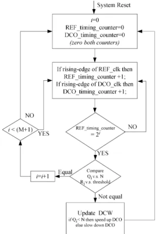
The dynamic frequency counting loop is a first-order system that uses a variable time period to estimate and tune the fre-quency of the DCO. Fig. 2 shows the loop control algorithm of the proposed DFC loop. The reference timing counter (REF_timing_counter) operates at the reference clock rate. The counter initially from zero counts up at every rising-edge
Fig. 3. Timestamp of frequency comparison.
of the reference clock. Similarly, the DCO timing counter (DCO_timing_counter) operates at the speed of the DCO output clock. The quotient and remainder vectors in the DCO timing counter are compared with the input multiplication factor ( ) when the reference timing counter is power-of-2 reference clock cycles. The sampling cycle time of the DFC loop control is defined as
(2) where represents the th DFC sampling state and is the cycle time of the input reference clock . The sampling cycle time is the timestamp performing the frequency com-parison of DCO clock output and is the maximum number of the DFC sampling state, which is shown in Fig. 3. If the re-sult of frequency comparison remains unchanged and the max-imum number of the DFC sampling state is less than
, both counters will continue frequency accumulation. Oth-erwise, the frequency error signal will be asserted to update current DCO control word (DCW) to adjust the DCO output frequency. Meanwhile, both reference timing counter and DCO timing counter are reset to zero.
Fig. 4 shows the basic structure of the dynamic frequency counting loop. It consists of four main functional units: refer-ence timing counter, DCO timing counter, DCO, and DFC loop controller. The reference timing counter serves as a variable timer for decision unit to estimate and control the DCO. The DCO timing counter performs as a frequency estimator of DCO output frequency. The DFC loop controller performs loop con-trol, frequency error accumulation, and gain control based on the measured frequency in the DCO timing counter. The DFC loop is a discrete-time sampled system implemented with all digital components. Consequently, the z-domain representation is the most natural method instead of using damping factor as indi-cated in (1) for analog PLL. Fig. 5 illustrates the signal model of the proposed clock generator with the DFC loop control. The transfer function of Fig. 5 is given by
(3)
where is the loop gain (i.e., and
, . From (3), it should be noted that should be placed in the range 0 2 for loop stability. Fig. 6 illustrates the pole displacement with gain variation. The max-imum value of is bounded by the loop gain . The DFC loop control is a first-order time-varying system. It only
accu-Fig. 4. Basic structure of the proposed dynamic frequency counting loop.
mulates the frequency error, thus, it generally features faster dy-namics and greater stability than higher order loops. The digital arithmetic comparator replaces conventional PFD conversion mechanisms. The variable frequency is determined by counting the number of rising-edge clock transitions of the dig-itally controlled oscillator. The sampled is compared with the multiplication factor ( ) in a digital arithmetic com-parator. If the comparison is equal, the comparator outputs 0; otherwise, it outputs 1 ( 1) if the reference frequency is faster (slower) than the DCO frequency. The result is then multiplied by gain . Then, the DCO’s output frequency is adjusted.
Fig. 7 shows the step response of the proposed clock gen-erator with DFC algorithm as compared with the sequential search. The step size of the sequential search is 1/128 (i.e., DCO is 8 bits) and the initial condition is set to 0.5 of normalized fre-quency to improve visualization. The proposed all-digital clock generator with DFC loop achieves fast locking in less than 10 iterations as illustrated in Fig. 7(a). By contrast, the sequential search requires at least 50 iterations to achieve frequency acqui-sition, as shown in Fig. 7(b). Furthermore, jitter variations will occur as indicated in Fig. 7(c) if the fine resolution of the DCO is inadequate.
B. Structure of the Reference and DCO Timing Counters
The structure of reference timing counter is a ripple counter with reset function. The length of reference timing counter is dependent on the maximum DFC sampling state to estimated DCO frequency. The structure of DCO timing counter is also a ripple counter with reset function. Therefore, most bits of the DCO timing counter are working in the low clock rate which can save power consumption. The length of the DCO timing counter is related to the multiplication factor ( ) and the length of ref-erence timing counter. If the maximum value of multiplication factor is , is formulated as
Fig. 5. Signal model of the proposed dynamic frequency counting loop.
Fig. 6. Pole displacement by gain variation.
Fig. 7. Step response of the proposed clock generator with DFC loop control versus sequential search. (a) Proposed. (b) Sequential search. (c) Jitter variation.
where represents the least integer greater than or equal to . If the length of the reference timing counter is , which is equal to the maximum number of the DFC sampling state, the length of the DCO timing counter equals . Fig. 8 shows the block diagram of the quotient and remainder vectors in the DCO timing counter with
Fig. 8. Structure of quotient and remainder vectors in the DCO timing counter.
bits. The values of the quotient and remainder vectors in the th sampling state are
(5) (6) where denotes the th bit of the DCO timing counter. The measured values of and in the DCO timing counter can then be calculated as follows:
(7) where denotes the cycle time of the DCO generated frequency.
C. Structure of the DFC Loop Controller
The structure of the DFC loop controller is shown in Fig. 9. The decision unit performs the digital arithmetic comparisons and updates the DCO control word (DCW). The decision unit compares the DCO timing counter based on frequency sampling period with power-of-2 input reference clock cycles as shown in Fig. 3. The decision unit also controls the frequency acquisition process and fine-tuning process. During the acquisition, loop gain control with binary search is applied to achieve fast locking. A multiplexer is used to select the DCO control code. Fig. 10(a)
Fig. 9. Structure of the proposed DFC loop controller.
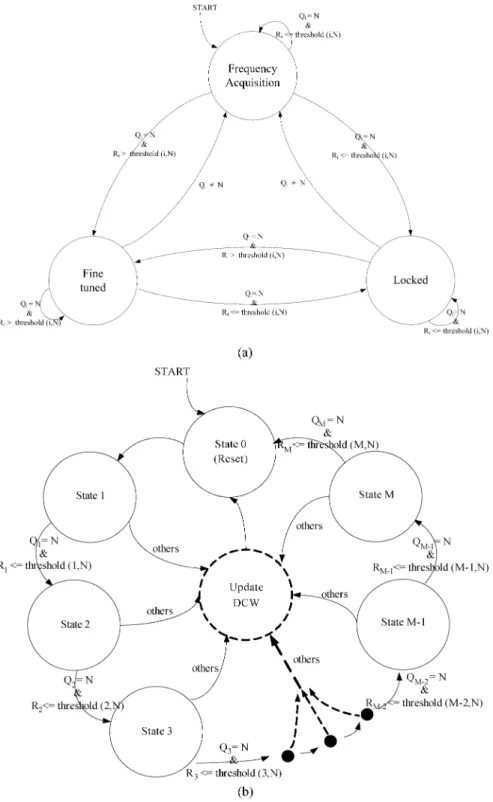
illustrates the state transition diagram of the DFC loop controller for frequency search. Fig. 10(b) shows the state of sampling period which is performed among acquisition, fine-tuned, and locked states. Sampling state 0 is the initial state, and both ref-erence timing counter and DCO timing counter are reset in this state. After a sampling period of , the DFC loop con-troller will switch from sampling state 0 into sampling state 1 for frequency comparison. If the quotient vector in DCO timing counter equals multiplication factor (N) and the frequency error in remainder vector is below the threshold region, sampling state 1 enters into sampling state 2 until sampling period and the DCO control word is left unchanged. Otherwise, the DFC loop controller changes the DCW depending on the fre-quency comparison result. Then, it also switches back to sam-pling state 0 and reset both reference and DCO timing counters. Similar operations as in sampling state 1 are performed in 2 to sampling states. When the DFC loop controller enters the maximum sampling state , it will automatically switch back to sampling state 0.
D. Threshold Decision
Considering the influence of jitter variation on frequency de-tection, the accumulation of frequency helps minimizing jitter effect in the frequency detection. A time varying with average processing and a threshold region scheme can be applied. For simplification and without losing generality, the average fre-quency period following cycles can be represented as
(8) where denotes the period of the jitterless clock or the named perfect frequency period, while represents the frequency jitter in the th cycle. All jitters are assumed to be independent and identically distributed (i.i.d) in statistics. The jitter factors can be reduced to an acceptable range when av-erage is large. Therefore, (7) can be rewritten using the
av-erage period of input reference frequency and DCO generated clock output frequency by using (8):
(9)
Both and denote the ideal period of DCO
output and input reference frequency. Similarly,
and represent the frequency jitter of the DCO gen-erated clock output and reference frequency in the th individual cycle. Therefore, a threshold value can be defined to solve the jitter variation in frequency detection. The resolution of fre-quency detection can be expressed as follows:
(10) The resolution of frequency detection is enhanced by increasing the number of sampling state and multiplication factor ( ). Therefore, the maximum value of sampling state is a tradeoff between loop gain and resolution of frequency detection.
III. CASCADED DFC LOOPS FOR
WIDEMULTIPLICATIONRANGE
Cascaded DFC loops are similar in design to multistage amplifiers. The dynamic frequency counting loop uses variable sampling period to estimate and adjust the DCO frequency, thereby enhancing the frequency detection resolution. How-ever, the loop gain in (3) caused by becomes large when multiplication factor ( ) has a wide range. The stable
Fig. 10. State transition of the proposed DFC loop controller. (a) State of frequency search. (b) State of sampling period.
region of is 0 2. To ensure that the loop remains stable for applications with wide multiplication ranges, the transfer function of (3) can be decomposed into
(11)
where denotes the loop gain of the first stage, and equals
, , .
Similarly, represents the loop gain of the second stage,
and equals and ,
. In these formulas, and represent the maximum numbers of sampling state in each DFC loop.
The DFC loop in the first stage generates a low-frequency output, or an intermediate frequency for the next stage. The output frequency range of a single DCO can be further divided
Fig. 11. Structure of the proposed clock generator with cascaded DFC loops.
into two DCO ranges. Hence, the loop gain and are easier to control in a stable region than using a single loop in (3). This approach not only decreases the length of the DCO timing counter and reference timing counter, but also the gain of the DCO. The proposed cascaded loops generate output frequency by averaging process in each stage. Hence, the noise influence or jitter variation on the DFC loop in the first stage has less influence on the output frequency of the DFC loop in the second stage.
A. System Block Diagram and Loop Parameters Design
Fig. 11 shows a system block diagram of the cascaded dy-namic frequency counting loops for wide multiplication range applications. The system consists of two DFC loops in series, called DFC loop 1 and DFC loop 2. The first DFC loop 1 gen-erates low-frequency output, or intermediate frequencies for the DFC loop 2. DFC loops 1 and 2 have different loop parameters and DCO requirements. DFC loop 1 only requires a low-fre-quency DCO 1 and a low-frelow-fre-quency detector. By contrast, the second stage is a high-resolution DCO 2, and also requires a high-resolution frequency detector. Both DFC loops 1 and 2 can be disabled, depending on output requirement, by the mode control. To prevent false locking, the DFC loop 2 is enabled after DFC loop 1 is locked in the acquisition process when two loops are employed. Because the DCO is divided into two DCO ranges, DCO 1 has a smaller control code than the DCO of a single loop, thus shortening the locking time.
To produce the maximum multiplication factor range over 10 000 and the lowest input frequency around 10 kHz, the multi-plication factor ( ) needs to be evenly distributed in the first and second stages. Therefore, the multiplication factor ( ) in the first stage’s DFC loop is in the range 2 255, and the multipli-cation factor ( ) in the second stage ranges 2 128. However, the lengths of the reference timing and DCO timing counters are different because of differences between and in (11). The variable sampling period in the DFC loop improves frequency detection as indicated in (10), but also affects the loop stability. After tradeoff of (10) and (11) with simulations, the length of reference timing counter is 4 bits in DFC loop 1 (i.e., ), and 8 bits in DFC loop 2 (i.e., ). Therefore, the DCO timing counters are 12 and 16 bits long in the first and second stages, respectively. The value of is set
to 8 in DFC loop 1, and 2 in DFC loop 2. Additionally, the least significant bit (LSB) resolutions of DCO 1 and DCO 2 are 65 ps and 0.55 ps, respectively.
IV. DESIGN OFDCO 1AND2FORCASCADEDDFC LOOPS
A. Structure of DCO 1
In the proposed design, the gain of DCO 1 is 65 ps/LSB, and the output frequency of DCO 1 is in the range 2 34 MHz (i.e., 29.4 500 ns). The proposed design only needs 13 binary weighted control bits, and achieves LSB resolution below 65 ps. The LSB resolution of DCO 1 can be easily implemented using standard cells in standard 0.18- m 1P6M CMOS process. Fig. 12 illustrates the basic structure of DCO 1, which is controlled by three cascading stages, range selection (DCW1[12:7]), coarse-tuning (DCW1[6:1]), and fine-tuning (DCW1[0]). The range selection and coarse-tuning stages are implemented with a path selector. The difference between these two stages is that the unit delay in range-tuning stage is larger than that in the coarse-tuning stage. To lower the chip area and power consumption of DCO 1, the unit delay in range-tuning stage is implemented with a delay cell in the cell library. Delay cells have longer MOS channel than normal cells, so have a much larger delay. A coarse-tuning delay cell is simply one buffer delay cell. The fine-tuning stage is 1-bit to control parallelized tri-state buffers.
B. High-Resolution DCO 2 With Digitally Controlled Varactors
The high-resolution DCO 2 is the key component in the proposed low-jitter clock generator for a wide multiplication range. To achieve 0.55 ps/LSB, [15] has developed a novel DCV using three-input NAND gates for DCO design. The DCV [15] uses the gate capacitance difference of NAND gates under different digital control inputs to build a digitally controlled varactor (DCV) as shown in Fig. 13(a). Fig. 13(b) shows the equivalent circuit of Fig. 13(a), an initial capacitance parallels with a capacitance difference with . The D input controls the capacitance in the output (Out) node. The marked transistor (M1) produces a large capacitance difference under different D states. 256 DCVs with different NAND gates are utilized to achieve high-resolution DCO. Therefore, the
Fig. 12. Structure of DCO 1.
Fig. 13. Using three-input NAND gate as DCV. (a) Circuit with digital control. (b) Equivalent circuit with1C capacitance.
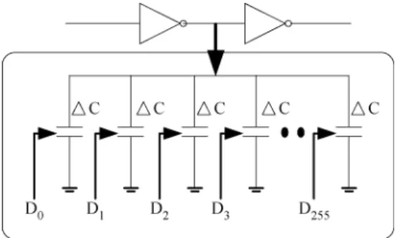
Fig. 14. 256 DCV’s in the fine-tuning stage of DCO 2.
LSB resolution of DCO 2 for fine-tuning stage can be improved by 256 times as compared with a simple buffer design.
The structure of DCO 2 is similar to DCO 1 shown in Fig. 12. It is also separated into three stages, namely range selection, coarse-tuning, and fine-tuning. The coarse-tuning stage is the same as that of DCO 1, and the fine-tuning stage is replaced by 256 DCV’s as shown in Fig. 14. DCO 2 has 16 bits of binary weighted control code . The coarse-tuning stage includes 32 buffer stages for delay-chain selection. The output frequency of DCO 2 is in the range 28 335 MHz. This architecture allows the operating frequency of DCO 2 to be modified easily to meet different specifications.
Both DCO 1 and DCO 2 are designed in gate-level Hardware Description Language (HDL) codes. The DFC loop controller
is also designed in HDL code and synthesized by a target li-brary. The final circuit layout is generated by auto placement and routing (APR) tools. As a result, the design cycle time is tremendously reduced during process migration.
V. EXPERIMENTALRESULTS
The proposed clock generator with cascaded DFC loops is fabricated and tested under different inputs reference fre-quencies and multiplication factors. LeCory LC584A is used to measure the output frequency with noisy digital circuitry. Fig. 15 illustrates the measured results with an input reference frequency of 19.26 kHz from an HP-3312 signal generator,
mul-tiplication factor (i.e., , ) and
test output divided by 2 at 134.7 MHz under a supply voltage of 1.8 V. The signal at Channel 2 displays the DCO gener-ated test output signal, while Channel D shows the long-term cycle-to-cycle jitter histogram. The measured rms jitter and peak-to-peak (P –P ) jitter of DCO 1 shown in Fig. 15(a) are 45 and 110 ps, respectively, and, the measured rms jitter and P –P jitter of DCO 2 shown in Fig. 15(b) are 76 and 200 ps, respectively. Fig. 16 shows the measured long-term cycle-to-cycle jitter of clock output versus multiplication factor ( ). The dashed line indicates the output jitter with the input reference clock set to 19.26 kHz and different multiplication factors. The solid line shows the output jitter with the test output clock fixed at 134.76 MHz and both multiplication factor ( ) and input reference clock are changed. The P –P
Fig. 15. Measured results withN = 13888 (N1 = 224, N2 = 62), REF clk = 10 kHz. (a) DCO 1 output @ 4.30 MHz 6 55 ps. (b). DCO 2 output @ 134.7 MHz6 100 ps.
jitter ratio is represented as the percentage of the output clock period, and is always less than 2.8% when multiplication factor ( ) is less than 13 888. The output clock frequency limits the performance owing to noise induced by the I/O pad transition. When the input clock frequency is set to 19.26 kHz, the P –P jitter ratio increases with the multiplication factor (N), and remains less than 2.8% of output clock period. The output clock period dominates the P –P jitter ratio as output frequency is increased.
The maximum multiplication factor of N1 is 224 instead of 255 owing to the overflow in the DCO timing counter 1, which causes false frequency locking. In addition, the overflow also limits the lowest input frequency of DCO 1. Similarly, overflow also restricts the multiplication factor of N2. To prevent over-flow, one more bit has to be extended in the most significant bit (MSB) of (5), as well as the DCO timing counter. Bit 0 is added to both the MSB of multiplication factors N1 and N2 for comparison.
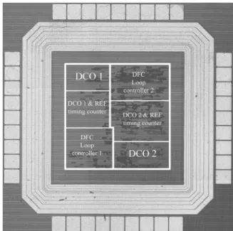
Fig. 17 shows a chip microphotograph of the proposed design. Table I lists the summary of chip features. The total gate count is
Fig. 16. Measured output cycle-to-cycle jitter versus multiplication factor (N) for fixed input clock= 19:26 kHz and fixed output clock = 134:7 MHz.
Fig. 17. Microphotograph of the proposed clock generator with cascaded DFC loops.
TABLE I SUMMARY OFCHIPFEATURES
6400 and the core area is m . Table II compares dif-ferent clock generators: analog PLL [2] and all-digital PLLs [5],
[7], [14]. The proposed all-digital clock generator with the pro-posed cascaded DFC loops has the largest multiplication range and the smallest chip area among the published PLLs, since it does not use analog capacitance and programmable divider. The work in [5] achieves faster locking than the proposed clock gen-erator, but it has worse jitter performance, less multiplication range, and higher cost.
VI. CONCLUSION
In this paper, a clock generator with cascaded dynamic frequency counting loops for wide multiplication range is pre-sented. The DFC loop is constructed with ripple counters and digital comparator which replaces conventional programmable divider and phase frequency detector. A threshold region is set for jitter variation on frequency detection. Different DCO requirements and loop parameters have been investigated in each DFC loop to maintain loop stability for wide-range multi-plication factor ( ). A test chip demonstrates that the proposed cascade DFC loops achieves the lowest input reference fre-quency at 19.26 kHz, and the corresponding P –P jitter is less than 2.8% of the output clock as the multiplication factor ( ) changes from 4 to 13 888. Hence, the proposed cell-based clock generator with the cascaded DFC loops lowers circuit cost and improves testability. The design can also be treated as a soft IP to accelerate turnaround time, making it suitable for system-on-chip applications.
ACKNOWLEDGMENT
The authors would like to thank their colleagues within the SI2 group of National Chiao Tung University for many fruitful discussions. The multiproject chip (MPC) support from National Chip Implementation Center is acknowledged as well.
REFERENCES
[1] H. T. Ahn and D. J. Allstot, “A low-jitter 1.9-V CMOS PLL for ultra-SPARC microprocessor applications,” IEEE J. Solid-State Cir-cuits, vol. 35, no. 5, pp. 450–454, May 1999.
[2] J. G. Maneatis, J. Kim, I. McClatchie, J. Maxey, and M. Shankarads, “Self-biased high-bandwidth low-jitter 1-to-4096 multiplier clock generator PLL,” IEEE J. Solid-State Circuits, vol. 38, no. 11, pp. 1795–1803, Nov. 2003.
[3] G. Yan, C. Ren, Z. Guo, Q. Ouyang, and Z. Chang, “A self-biased PLL with current-mode filter for clock generation,” in IEEE Int. Solid-State Circuits Conf. (ISSCC) Dig. Tech. Papers, Feb. 2005, pp. 420–421. [4] K. L. Wang, E. Fayneh, E. Knoll, R. H. Law, C. H. Lim, R. J. Parker,
F. Wang, and C. Zhao, “Cascaded PLL design for a 90 nm CMOS high-performance microprocessor,” in IEEE Int. Solid-State Circuits Conf. (ISSCC) Dig. Tech. Papers, Feb. 2004, pp. 346–347.
[5] T. Watanabe and S. Yamauchi, “An all-digital PLL for frequency multi-plication by 4 to 1022 with seven-cycle lock time,” IEEE J. Solid-State Circuits, vol. 38, no. 2, pp. 198–204, Feb. 2003.
[6] M. Zarubinsky, K. Berman, and E. Zipper, “Signal Generator, and Method,” U.S. Patent 6,380,811, Apr. 30, 2002.
[7] J. Lin, B. Haroun, T. Foo, J.-S. Wang, B. Helmick, S. Randall, T. May-hugh, C. Barr, and J. Kirkpartick, “A PVT tolerant 0.18 MHz to 600 MHz self-calibrated digital PLL in 90 nm CMOS process,” in IEEE Int. Solid-State Circuits Conf. (ISSCC) Dig. Tech. Papers , Feb. 2004, pp. 488–489.
[8] R. B. Staszewski et al., “Digitally controlled oscillator (DCO)-based architecture for RF frequency synthesis in a deep-submicrometer CMOS process,” IEEE Trans. Circuits Syst. II, Analog Digit. Signal Process., vol. 50, no. 11, pp. 815–828, Nov. 2003.
[9] J. Dunning, G. Garcia, J. Lundberg, and E. Nuckolls, “An all-digital phase-locked loop with 50-cycle lock time suitable for high perfor-mance microprocessors,” IEEE J. Solid-State Circuits, vol. 30, no. 4, pp. 412–422, Apr. 1995.
[10] I. Hwang, S. Lee, and S. Kim, “A digitally controlled phase-locked loop with a digital phase-frequency detector for fast acquisition,” IEEE J. Solid-State Circuits, vol. 36, no. 10, pp. 1574–1581, Oct. 2001. [11] T. Olsson and P. Nilsson, “A digitally controlled PLL for SoC
applica-tions,” IEEE J. Solid-State Circuits, vol. 39, no. 5, pp. 751–760, May 2004.
[12] M. Combes, K. Dioury, and A. Greiner, “A portable clock multiplier generator using digital CMOS standard cells,” IEEE J. Solid-State Cir-cuits, vol. 31, no. 7, pp. 958–965, Jul. 1996.
[13] T.-Y. Hsu, C.-C. Wang, and C.-Y. Lee, “Design and analysis of a portable high-speed clock generator,” IEEE Trans. Circuits Syst. II, Analog Digit. Signal Process., vol. 36, no. 10, pp. 1574–1581, Oct. 2001.
Pao-Lung Chen (S’01–M’05) received the B.S.
degree from Chung-Yuan Christian University, Chung-Li, Taiwan, R.O.C., in 1987, and the M.S. degree from Texas A&M University, College Sta-tion, TX, in 1992, both in electrical engineering. He received the Ph.D degree from the Department of Electronics Engineering, National Chiao Tung University, Hsinchu, Taiwan, in 2005.
He is an Assistant Professor in the Department of Electronics Engineering, Chin-Min Institute of Tech-nology, Toufen, Taiwan. His interests include all-dig-ital PLL design, cell-based frequency synthesizers, and all-digall-dig-ital DLL design.
Ching-Che Chung (S’02–M’05) received the Ph.D.
degree in electrical engineering from National Chiao Tung University, Hsinchu, Taiwan, R.O.C., in 2003.
Since January 2004, he has been a Postdocto-rial Researcher in the Department of Electronics Engineering, National Chiao Tung University. His research interests include system-on-chip design methodologies, low-power wireless baseband pro-cessor design and high-speed interface circuit design.
Engineering and the Institute of Electronics, National Chiao-Tung University, Hsinchu, Taiwan, in 2006. His research interests include analog integrated circuits and RF integrated circuits design.
Chen-Yi Lee (M’90) received the B.S. degree from
National Chiao Tung University, Hsinchu, Taiwan, R.O.C., in 1982, and the M.S. and Ph.D. degrees from Katholieke University Leuven (KUL), Belgium, in 1986 and 1990, respectively, all in electrical engi-neering.
From 1986 to 1990, he was with IMEC/VSDM, working in the area of architecture synthesis for DSP. In February 1991, he joined the faculty of the Electronics Engineering Department, National Chiao Tung University, where he is currently a Pro-fessor and Department Chair. His research interests include VLSI algorithms and architectures for high-throughput DSP applications. He is also active in various aspects of high-speed networking, system-on-chip design technology, very low-power designs, and multimedia signal processing. He served as the Director of Chip Implementation Center (CIC), an organization for IC design promotion in Taiwan. He is now the microelectronics program coordinator of Engineering Division under National Science Council of Taiwan.