LOG filter based inspection of Cluster Mura and
Vertical-Band Mura on liquid crystal displays
Hsin-Chia Chen*
a, Li-Te Fang
a, Louis Lee
b,
Chao-Hua Wen
b, Shang-Yuan Cheng
c, and Sheng-Jyh Wang
a aInstitute of Electronics, National Chiao Tung University, Taiwan 30050
b
Taiwan TFT-LCD Association, Taiwan 30050
cIndustrial Technology Research Institute, Taiwan 30050
ABSTRACT
In this paper, we propose the use of Laplacian of Gaussian (LOG) filters in the detection of Cluster Mura defects and Vertical-Band Mura defects on Liquid Crystal Displays. To detect Cluster Mura defects, 2-D LOG filters with their shapes matching the shapes of Cluster Mura are adopted. The optimal threshold for the detection of Cluster Mura is determined based on the SEMU formula. On the other hand, to detect Vertical-Band Mura, a 1-D LOG filter is used over the projected 1-D intensity profile to check if the variation tendency of the intensity profile is changed. The portions with inconsistently intensity variation are regarded as the portions where V-Band Muras occur. The simulation results demonstrate the LOG filters are very useful in the detection of Mura defects.
Keywords: Laplacian of Gaussian, Mura defects, Mura detection, SEMU
1. INTRODUCTION
Recently, Liquid Crystal Displays (LCDs) have been receiving increasing market attention because of their going-down prices and their dramatically improved visual quality. Among several characteristics regarding the visual quality of LCDs, the front-of-screen (FOS) quality of LCDs is the essential one. Most existing FOS quality tests depend on the perception of human eyes. However, human inspection needs higher labor power and usually causes inefficient production and inconsistent inspection. Instead of human inspection, automatic inspection that employs efficient algorithms over photographed images could be a reasonable and reliable way to evaluate the FOS quality of LCDs. Recently, several efforts have been spent on the fulfillment of defect classification and the establishment of quality evaluation standards1-2. For example, the Video Electronics Standards Association (VESA) has been carrying activities
related to standards for classifying defects1, while the Semiconductor Equipment and Materials International (SEMI)
have spent a lot of efforts on the standardization of defect quantification2. Nevertheless, although the automatic
inspection of FOS quality is highly demanded, there are relatively few efforts spent on the development of defect detection algorithms3-6.
In this paper, we focus on the development of detection algorithms for the inspection of the FOS quality of an active matrix thin-film transistor liquid crystal display (AM LCD). Fig. 1 illustrates the cross-section of an AM TFT-LCD. According to Y. Mori’s classification3, various causes, as listed in Table 1, could produce defects. Basically, an
LCD display includes two essential components: 1) Cell Unit and 2) Backlight Unit. In the cell unit, there are five elements: (1) liquid crystal, (2) thin-film-transistor (TFT) array, (3) color filters, (4) glasses and (5) polarizer. In general, the functionality of cell unit is to make the RGB color switching at each pixel controllable. On the other hand, in the backlight unit, there are four basic elements: (1) lamp, (2) light pipe, (3) reflective film and (4) optical film. Generally, the functionality of backlight unit is to produce uniform light.
In the inspection of FOS quality, the so-called Mura defects greatly influence the FOS quality1. The Mura defects are defined as the visible imperfections of the FOS of a display screen in active use. As shown in Table 1, Mori et al3
listed several causes of Mura defects in TFT-LCD. Usually, the manufacturing performance of every component in the cell unit or the backlight unit will affect the appearance of Mura defects. A superior manufacture process will cause less Mura defects, while an inferior manufacture process will induce more visible Mura defects. Usually, the non-uniformity in various kinds of components induces different kinds of Mura defects.
Figure 1: Cross-section of an active matrix TFT-LCD.
Table 1. Causes of Mura defects for TFT-LCD3
Basic Unit Causes of Mura
(1) Non-uniform gap between glasses (2) Non-uniform color of color filter (3) Non-uniform density of
liquid crystal Cell unit
(4) Non-uniform thickness of TFT array layer
(5) Wrinkled optical filter (6) Non-uniform lamp’s rays Backlight unit
(7) Warped light pipe
In general, Mura defects appear as low contrast, non-uniform brightness regions. They are typically larger than a single pixel when the screen is driven to a constant gray level. As mentioned above, different kinds of causes produce different kinds of Mura defects. Therefore, to detect all kinds of Mura defects, it would be difficult to develop a single universal algorithm. In this paper, we will consider two major kinds of Mura defects, Cluster Mura and Vertical-Band Mura, which occur normally in the FOS of LCDs In Section 2, we will introduce the photography of FOS image. In Section 3, the detection of Cluster Mura will be discussed. Then we will consider Vertical-Band Mura detection in Section 4. Finally, conclusions will be given in Section 5.
2. PHOTOGRAPHY OF FOS IMAGES
Fig. 2(a) shows the prototype of our automatic inspection system. In this system, we have an LCD panel that is under test, a CCD camera to capture the FOS image of the LCD panel, and a computer to execute Mura detection algorithms. In the inspection process, the LCD under test is vertically placed on the apparatus. Each time, the LCD is driven by a pattern generator to display a certain gray level image pattern. Then, the camera will capture an FOS image for this specific pattern. The FOS image is transmitted to the computer to be stored and to be inspected with a set of Mura detection algorithms.
(a) Inspection prototype (b) Flowchart of LCD inspection Figure 2: The prototype of the LCD inspection system.
At markets, 15-inch and 17-inch LCD panels are the mainstream for desktop displays and notebook displays. In fact, the manufacture processes in these two types of LCD panels are quite similar. Hence, the appearances of Mura defects are also similar. Both types of LCD panels can be inspected by this prototype system. Moreover, to mimic the performance of human inspection, the specifications of CCD camera are chosen to have a more than 12-bit dynamic range and a spatial resolution of 1532 × 1024 pixels.
2.1 Aliasing
In the photography process, aliasing usually occurs when the lens of camera is focused on the center of the FOS. Fig. 3(a) shows the aliased image. Fig. 3(b) shows the enlarged image of the portion inside the red rectangular in Fig. 3(a). As shown in Fig. 3(b), the lattice-like pattern occurs when the camera lens is in focus. This lattice-like pattern will not only increase the difficulty in automatic inspection but also influence the inspection results of Mura defects.
To eliminate the aliasing effect, several anti-aliasing approaches have already been published or patented7,8. These
approaches usually require some additional accessories and may cause image blurring. Among these approaches, we adopt the de-focusing approach, which may eliminate the aliasing effect without any additional accessories. In this approach, we focus the camera lens on the FOS of LCD first, followed by de-focusing the camera lens till the lattice-like pattern disappears. Although this method still causes the blurring of the FOS image, it demands no extra expense. In Fig. 3(c), we show the de-focused image of Fig. 3(a). It can be easily seen that the lattice-like pattern does disappear.
Figure 3: Aliasing in the photography process. 2.2 Cluster Mura and V-Band Mura
Among several kinds of Mura defects, the detection of two major kinds of Mura defects, Cluster Mura and Vertical Band (V-Band) Mura, will be taken into account in this paper. As mentioned before, Mura defects appear as non-uniform brightness regions in the FOS of an LCD. Nevertheless, not all kinds of Mura defects appear in the similar manner. For example, Cluster Mura usually appears as a cluster of several points locating within a small area. Dust or small particles appearing at the liquid crystal layer or TFT layer may induce this kind of Mura defects. As shown in Fig. 4(a)(c), a round-type Cluster Mura defect locates at (x=750, y=820), while a rectangular-type Cluster Mura defect appears as a narrow region ranging from (x=200, y=720) to (x=600, y=720). On the other hand, V-Band Mura usually appears as a wide vertical strip with either brighter or darker brightness with respect to the uniform background. As shown in Fig. 4(e), a V-Band Mura is centered around x=850. The cause of V-Band Mura usually comes from non-uniform thickness of components, such as non-non-uniform thickness of glasses in the cell unit. In comparison, Cluster Muras usually appear in a local area, while V-Band Muras usually occupy a larger area. Therefore, not all kinds of Mura defects appear in the same scope. In fact, the appearance model of Cluster Mura is quite different from that of V-Band Mura. Therefore, it would be impractical to detect both types of Muras based on a single universal algorithm.
In the following sections, we will present the use of different approaches to deal with these two kinds of Mura defects. In spite of the use of different approaches, these approaches actually share the same kernel: the Laplacian of Gaussian (LOG) filter. The LOG filter, which compares the intensity of the target with the intensity of the surroundings,
(a) Round-type Cluster Mura (c) Rectangular-type Cluster Mura (e) V-Band Mura
(b) Detection result of (a) (d) Detection result of (c) Figure 4: Cluster Mura and V-Band Mura.
will be demonstrated to be very useful in the development of Mura detection algorithms. To detect Cluster Mura defects, an approach with the 2-D LOG filter will be presented in Section 3. To detect V-Band Mura, on the other hand, an approach with a 1-D LOG filter will be presented in Section 4.
3. INSPECTION OF CLUSTER MURA
3.1 Cluster Mura detection
To detect Cluster Mura defects, 2-D LOG filters are adopted. In the detection of Cluster Mura, the Laplacian of Gaussian (LOG) filter compares the intensity of the target with the intensity of the uniform background. At a Cluster Mura, there is an apparent intensity difference between the Cluster Mura defects and the uniform background. Hence, it is expected that the linear LOG filters are applicable to the detection of Cluster Mura defects.
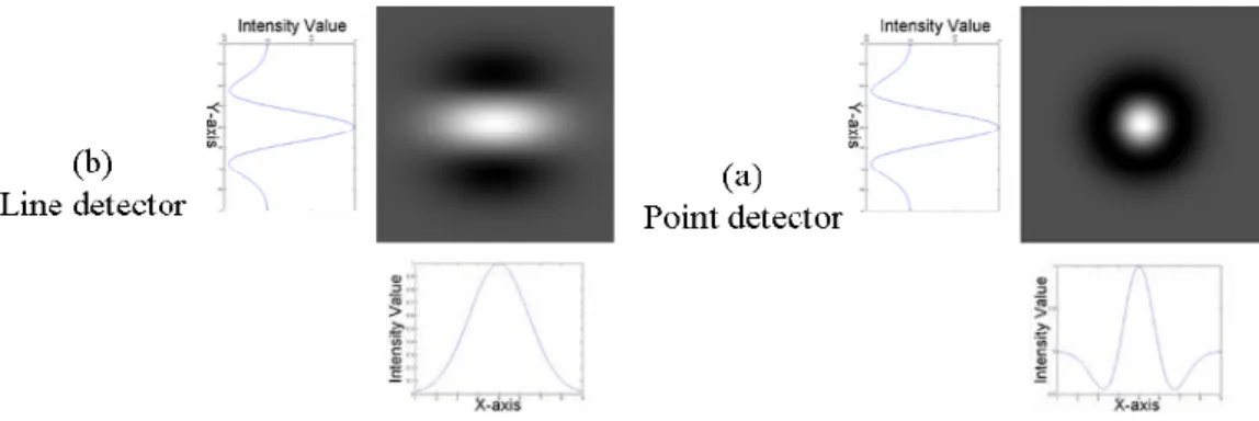
Usually, there are two types of Cluster Mura defects: round-type Cluster Mura and rectangular-type Cluster Mura. To detect round-type Cluster Mura defects, we use a 2-D round-type LOG filter as shown in Fig. 5(a), whose shape matches the shape of the round-type Cluster Mura. The formula of the round-type LOG filter could be formulated as
(
)
( , ; , , ) ) , ( xx yy x y Round LOG x y N x y filter = ∇ +∇ 0σ σ , (1) where N(x,y;0,σ
x,σ
y) denotes a 2-D Gaussian function with zero mean and standard deviations σx and σy. If we setσx = σy= σ, then there is only one parameter to be assigned by users. In Section 3.3, we will discuss the rule of
Figure 5: 2-D LOG filters for point detection and line detection.
To detect rectangular-type Cluster Muras, we adopt a 2-D rectangular-type LOG filter, whose shape matches the shape of the rectangular-type Cluster Mura as shown in Figure 5(b). The corresponding formula of the round-type LOG filter could be formulated as
( )
( , ; , , ) ) , ( yy x y LOG x y N x y filterRectangular = ∇ 0σ
σ
. (2) In (2), there are two parameters, σx and σy. If the ratio of these two parameters, r=σx /σy, is fixed, then there is onlyone parameter left to be assigned by users.
With the round-type LOG filters and the rectangular-type LOG filters, the round-type Cluster Mura defects and the rectangular-type Cluster Mura could be “matched” and detected. The detection result of Fig. 4(a) is given in Fig. 4(b), in which the blue region denotes the area of no interest while the red area denotes the detection result of Cluster Mura. Similarly, the detection result of Fig. 4(c) is given in Fig. 4(d).
3.2 SEMU formula
To evaluate the blemish degree of the Cluster Mura defects, the SEMU formula2, which is described in (3).
) . . (1970.33+072 = ≡ A C C C SEMU x jnd x , (3)
where Cx is the average contrast of Mura, Cjnd the just noticeable contrast of Mura, and A the area of Mura. Modified
versions of this SEMU formula have been proposed9,10. In the SEMU formula and also its modified versions, there are
two main factors: 1) contrast of Mura defects and 2) area of Mura defects. A larger value of SEMU indicates a more serious blemish. As indicated in (3), either a larger contrast of Mura defect or a larger area of Mura defect will cause a larger degree of blemish.
3.3 Optimal threshold with SEMU formula
As mentioned in Section 3.2, to detect round-type Cluster Mura, round-type LOG filters are adopted. As illustrated in Fig. 6, we assume Additive White Gaussian Noise (AWGN) is involved in the photography process.
In general, the output of filtered Cluster Mura defect could be described in (4), ) , ( ) , ( ) , (x y Mura x y filter x y Output Round LOG Cluster ⊗ = . (4) According to the SEMU formula2, the round-type Cluster Mura could be formulated as
− + × = 1 2 2 2 r y x u h y x MuraCluster( , ) . (5)
where r is the radius of the round-type Cluster Mura, and u(t) is the step function defined as
( )
≥ < = 0 1 0 0 t t t u , , . (6)Combining (4) with (5), we could derive (7),
0 0 = = = = = =y = Cluster ⊗ LOG x y x y x y x filter y x Mura y x Output , ) , ( ) , ( ) , ( σ σ σ exp( 2) 2 4 2 2 4σ σ r hr − − = . (7) On the other hand, the variance of the filtered noise could be estimated as (8),
(
)
∫ ∫
= Var H u v dudv
VarFiltered Noise Estimated Noise
2 ) , ( _ _ (8)
where VarEstimed_Noise denotes the variance of the AWGN noise produced in the photography process and H(x,y)
represents the round-type LOG filter.
If combining (1) and (8), we could derive (9),
7 32πσ Noise Estimated Noise Filtered Var Var _ _ = . (9)
To optimize the Signal to Noise Ratio (SNR) in (10),
(
)
noise Filtered Var_ _ 2 Output SNR≡ (10) which is defined as the square power of the output response magnitude over the variance of the filtered noise, we could derive the relationship between the radius of the round-type Cluster Mura and the standard deviation of the optimal matched filter. The relationship is found to beσ
2 1 =
r . (11) As mentioned before, to evaluate the blemish degree of Cluster Mura, the SEMU formula is suggested2. If we
assume the SEMU value to be a constant S, the relation between Mura contrast and Mura area could be derived as the following If we define S A h = + . ) . (1970.33 072 , (12) then
(
)
S y x Output( , )x y 0.2126 8/3 0.09 2 exp( 1/4) 0=− + − − − = = σ σ . (13)According to the Bayesian formula, the optimal threshold for the detection of Mura is derived in (14) (See Fig. 7). Once the constant S is fixed and the standard deviation in the Gaussian function is determined, the optimal threshold could be decided based on (14),
(
)
Sthreshold 0.2126 / 0.09 exp( 1/4)
2
1×− 83+ 2 −
= σ− σ− . (14)
4. INSPECTION OF V-BAND MURA
4.1 V-Band Mura detection
Unlike Cluster Mura, V-Band Mura usually appears with a large area. Therefore, the use of a 2-D LOG filter whose shape “matches” the shape of V-Band Mura is no longer a suitable way for efficient inspection. In general, as the size of filters increases, the computation time increases dramatically.
Hence, in this paper, we take a different approach to detect V-Band Mura defects. Fig. 8(b) shows the FOS image with three contours, in which the pixels with similar intensity values are drawn in the same color. The pixels with red color have larger intensity values than the pixels with brown color. At the meanwhile, the intensity values of pixels with brown color are larger than the intensity values of pixels with black color. In Fig. 8(b), we could see that the tendency of the intensity variation along the vertical direction is approximately the same at any horizontal coordinate. Basically, with a fixed horizontal coordinate, the intensity in the center area tends to be larger than the intensities on the two sides. Due to this similarity in the intensity variation along the vertical direction, the operation of intensity projection along the vertical direction will not affect the tendency of intensity variation along the horizontal direction.
Hence, in our approach, the projection method is applied first along the vertical direction. As shown in Fig. 8(d), the blue dotted line represents the intensity profile projected along the y-axis. With this projected intensity profile, we could easily see that the profile around x=850 have a significant variation. To detect this significant variation, we first estimate a smooth curve from the original profile. To estimate the smooth curve, some specific sample points should be used. Since zero-crossing points in the intensity profile represent the points with no significant curvature variation. Therefore, we use the zero-crossing points as the sample points in our proposed algorithm to estimate the smooth curve from the original intensity profile.
To extract zero-crossing points, we use a 1-D LOG filter to estimate the curvature of the profile. With a 1-D LOG filter which is formulated as (12), we can extract zero-crossing points, which are represented in green points in Fig. 8(d).
( )
( ; , ))
( xx x
LOG x N x
filter = ∇ 0σ . (12) With these zero-crossing points, a 2-order curve fitting method is adopted to generate the smooth intensity tendency curve, which is shown as the pink curve in Fig. 8(d). Comparing the smooth curve to the original curve, we define the fractions with large deviation to the original curve to be the locations of V-Band Mura defects. Fig. 8(c) shows the detection result of V-Band Mura in Fig. 8(a), with the red box circling the area of V-Band Mura.
Figure 8: V-Band Mura detection. 4.2 FOS surface reconstruction
To verify the V-Band detection approach, we reconstruct the imaginary FOS image with the smooth intensity variation tendency. In Fig. 9(c), with these zero-crossing points extracted by the 1-D LOG filter, Spline interpolation is adopted to estimate the smooth intensity variation tendency that is represented in red curve in Fig. 9(c). With this smooth intensity variation tendency, we can reconstruct the smoothed FOS surface, as shown in Fig. 9(b). It can be seen that there is no V-Band-like Mura occurring in Fig. 9(b).
5. CONCLUSION
In this paper, we suggest the use of 2-D round-type/rectangular-type LOG filters to detect round-type/rectangular-type Cluster Mura defects. With 2-D LOG filters, the optimal threshold is analyzed with the SEMU formula. Also, we propose a curvature test approach to detect V-Band Mura defects. In the curvature test approach, a 1-D LOG filter is used to generate a smooth curve that represents the curvature tendency of the 1-D projected profile. With this smooth curve, V-Band Mura defects can be detected easily. In simulation, the results demonstrate the LOG filters are very useful in the development of detection algorithms for the inspection of Mura defects.
6. REFERENCES
1. Video Electronics Standards Association (VESA): Flat Panel Display Measurements Standard, version 2.0, p.78. 2. Semiconductor Equipment and Materials International (SEMI) standard, “New Standard: Definition of Measurement
Index (SEMU) for Luminance Mura in FPD Image Quality Inspection,” draft number: 3324, pp. 1-6, 2002.
3. Y. Mori, K. Tanahashi, and S. Tsuji, “Quantitative Evaluation of Visual Performance of Liquid Crystal Displays,” Proceedings of the Algorithms and Systems for Optical Information Processing (The International Society for Optical Engineering), vol. 4113, pp. 242-249, 2000.
4. Y. Mori, R. Yoshitake, T. Tamura, T. Yoshizawa and S. Tsuji, “Evaluation and Discrimination Method of "mura" in Liquid Crystal Displays by Just Noticeable Difference Observation,” SPIE (The International Society for Optical Engineering) Proceedings, vol. 4902, pp. 715-722, 2002.
5. W. K. Pratt, S. S. Sawkar, and K. O'Reilly, “Automatic Blemish Detection in Liquid Crystal Flat Panel Displays,” SPIE (The International Society for Optical Engineering) Proceedings, vol. 3306, pp. 2-13, 1998.
6. V. Gibour and T. Leroux, “Automated, Eye-like Analysis of Mura Defects,” Proceedings of SID, pp. 1440-1443, 2003.
7. Intel corp. patent, “Anti-Aliasing Diffractive Aperture and Optical System using the same,” US. Patent: 5940217, Aug. 1999.
8. “Aliasing reduction in discrete imaging system using pupil function controlling,” Proceedings of Acta Optica Sinica, 19(3), pp.289-294, 1999.
9. D. G. Lee, I. H. Kim, M. C. Jeong, B. K. Oh, and W. Y. Kim, “Mura Analysis Method by Using JND Luminance And the SEMU Definition,” Proceedings of SID, pp. 1467-1470, 2003.
10. T. Tamura, M. Baba and T. Furuhata, “Effect of the Background Luminance on Just Noticeable Difference Contrast of ‘Mura’ in LCDs,” Proceedings of SID, pp. 1527-1530, 2003.