Contents lists available atScienceDirect
Superlattices and Microstructures
journal homepage:www.elsevier.com/locate/superlatticesStructure and properties of GZO thin films grown on ZnO
buffer layers
C.Y. Chu
a, C.H. Huang
b, L.M. Kao
c, C.P. Chou
a, C.Y. Hsu
b, C.W. Chen
b,
D.Y. Chen
d,∗aDepartment of Mechanical Engineering, National Chiao Tung University, Taiwan, ROC
bDepartment of Mechanical Engineering, Lunghwa University of Science and Technology, Taiwan, ROC cDepartment of Mechatronic Technology, Tungnan University, Taiwan, ROC
dDepartment of Mechanical Engineering, Hwa Hsia Institute of Technology Taipei, Taiwan, ROC
a r t i c l e i n f o Article history:
Received 12 June 2010 Received in revised form 21 November 2010 Accepted 5 December 2010 Available online 10 December 2010 Keywords:
Transparent conductive oxide Buffer layer
Growth rate
Grey relational analysis
a b s t r a c t
Thin gallium-doped zinc oxide (in GZO the Ga2O3 contents are
approximately 3 wt%) films having different ZnO buffer layers were deposited using radio frequency (rf) magnetron sputtering. The use of a grey-based Taguchi method to determine the processing parameters of ZnO buffer layer deposition has been studied by con-sidering multiple performance characteristics. A Taguchi method with an L9orthogonal array, signal-to-noise (S/N) ratio, and
anal-ysis of variance (ANOVA) is employed to investigate the per-formance characteristics in the deposition operations. The effect and optimization of ZnO buffer deposition parameters (rf power, sputtering pressure, thickness, and annealing) on the structure, morphology, electrical resistivity, and optical transmittance of the GZO films are studied. Annealing treatment and reduction in thickness resulted in a decrease in root-mean-square (RMS) sur-face roughness of the ZnO buffer layer. Using the optimal ZnO buffer layer obtained by the application of the grey-based Taguchi method, the electrical resistivity of GZO films was decreased from 2.94×10⁻³to 9.44×10⁻⁴cm and the optical transmittance in
the visible region was slightly increased from 84.81% to 85.82%. © 2010 Elsevier Ltd. All rights reserved.
∗Corresponding author. Fax: +886 2 29436521.
E-mail address:[email protected](D.Y. Chen).
0749-6036/$ – see front matter©2010 Elsevier Ltd. All rights reserved.
1. Introduction
Zinc oxide (ZnO) has been widely used for many applications, such as surface acoustic wave devices, liquid crystal displays, energy efficient windows, and transparent electrodes, due to its excellent electrical and optical properties [1,2]. Intrinsic ZnO is an n-type wide-bandgap (3.3 eV) semiconductor oxide with a hexagonal wurtzite structure. Under standard conditions, its resistivity is high. In order to enhance its electrical and optical properties, ZnO is commonly doped with Group III elements (B, Al, Ga or In) [3]. The incorporation of these elements into the ZnO lattice can stabilize the film at high temperatures and increase its electrical conductivity [4]. Among metal dopants, Ga doping seems to be the most successful and promising due to the similar atomic radius of Ga3+to Zn2+and its lower reactivity to oxygen [5]. For the deposition of Ga2O3-doped ZnO films, several techniques have been developed, such as radio frequency magnetron sputtering [6], chemical vapor deposition [7], ion plating systems [8], spray pyrolysis [9], and pulsed laser deposition [10].
The Taguchi method is a systematic application of design and analysis experiments for the purpose of designing low-cost products of improved quality [11]. The mixed orthogonal table in the Taguchi quality design derives important deposition factors. A statistical analysis of signal-to-noise (S
/
N) ratio is followed by performing an analysis of variance (ANOVA) [12].Depending on the particular type of characteristics involved, different S
/
N ratios may be applicable, including ‘‘lower is better’’ (LB), ‘‘nominal is best’’ (NB), and ‘‘higher is better’’ (HB). The S/
N ratios were calculated using the following equations [11]:η =
10 log(
S/
N ratio)
(1) HB:(
S/
N ratio) =
1σ
2σ
2=
1 n
1 y2 1+
1 y2 2+ · · · +
1 y2 n
(2) LB:(
S/
N ratio) =
1σ
2σ
2=
1 n(
y 2 1+
y22+ · · · +
y2n)
(3)where ynis the characteristic property, n is the number of repeated experiments, and
η
denotes the observed value, i.e., the calculated value of the S/
N ratio. The unit of the S/
N ratio is the decibel (dB), which is frequently used in communication engineering.In this paper, we report on the effects of the deposition parameters of the ZnO buffer layer on the surface morphology and the structural and optoelectronic properties of GZO thin films grown on glass by rf magnetron sputtering. Grey relational analysis is used to investigate multiple performance characteristics of the Taguchi method for the optimized deposition process within a limited number of experiments [13].
We investigate the impact of four parameters (control factors) each at three levels (1–3), namely rf power (A), sputtering pressure (B), film thickness (C), and annealing treatment (D) on the ZnO buffer layer quality, as can be seen inTable 1. In other words, an L9(34, with four columns and nine rows) orthogonal array was employed [14].Table 1shows the deposition parameters of the ZnO buffer layer, factors and levels, andTable 2displays the coating parameters of the GZO films to be grown on ZnO buffered glass.
2. Experimental
Thin GZO films and ZnO buffer layers were deposited by rf magnetron sputtering with a base pressure of 0
.
67×
10−3 Pa. The diameter and thickness of the sputtering targets (commercially available hot-pressed and sintered targets) of GZO and ZnO were 50.8 mm and 6 mm, both of 99.995% purity. The doping amount of Ga2O3 in ZnO powder used in this study was 3 wt% [15]. Before the experiment began, the target was pre-sputtered for 10 min in order to remove any contamination. The glass (Corning 1737) substrates were cleaned by following a standard cleaning procedure (TCE-acetone-methanol-ethanol-DI water). The magnetron sputtering system is microprocessor-controlled.The film thickness was measured using a surface profilometer (
α
-step, AMBIOS XP-1). The surface morphologies were analyzed by an atomic force microscope (AFM, PSIA-XE-100). Structural propertiesTable 1
Deposition parameters of ZnO buffer layer, factors, and levels.
Substrate Corning 1737 glass
Target ZnO, 99.995% purity, 50.8 mm diameter
Gas Argon (99.995%)
Base pressure 0.67×10⁻³Pa
Substrate-to-target distance 90 mm
Substrate temperature Room temp.
Substrate rotate vertical axis 10 rpm
Symbol Control factors Level 1 Level 2 Level 3
A rf power (W) 50 100 150
B sputtering pressure (Pa) 0.13 0.67 1.33
C ZnO buffer thickness (nm) 50 150 300
D post-annealing temperature (°C) None 200 400
Note: The post-annealing time was 30 min, and the annealing was performed in ambient vacuum. Table 2
Deposition parameters of GZO film (with and without ZnO buffer).
Target GZO contained 3 wt% Ga2O3, 99.995% purity, 50.8 mm diameter
Gas Argon (99.995%)
Base pressure 0.67×10⁻³Pa
Substrate rotate vertical axis 10 rpm
Substrate-to-target distance 90 mm
Substrate temperature Room temp.
rf power 100 W
Sputtering pressure 0.67 Pa
GZO thickness 600 nm
Deposition rate 5.20 nm/min
were analyzed using Cu-K
α
radiation (Rigaku-2000 X-ray diffraction (XRD) spectrometer). Electrical resistivity was measured by the four-point probe method (Mitsubishi chemical MCP-T600). Optical transmittance measurements in the wavelength range of 300–800 nm were made by using a UV–VIS spectrophotometer.3. Results and discussion
3.1. Properties of ZnO buffer
In this experiment, the growth rate of ZnO films is defined as the thickness of ZnO films (nm) divided by deposition time and can be expressed in nm
/
min. The root mean square (RMS, nm) is employed to denote surface roughness. In the Taguchi method, the signal-to-noise (S/
N) ratio is the most important component of a parameter design; the term ‘signal’ represents the desired target for good products and the term ‘noise’ represents the undesired value.Table 3shows the experimental results and S/
N ratios for the growth rate and AFM root mean square (RMS) surface roughness of ZnO buffer grown on glass (the experiments were repeated two times). The growth rate (higher is better) and the corresponding S/
N by using Eqs.(1)and(2). The surface roughness (lower is better) and the corresponding S/
N by using Eqs.(1)and(3). The S/
N ratio graph it is always ‘‘larger is better’’ and a positive number for S/
N is larger than a negative number.Table 4illustrates the results of analysis of variance (ANOVA) for growth rate and surface roughness of the ZnO buffer grown on glass. The ANOVA table shows the relative importance of the deposition parameters affecting the quality characteristics [16]. As can be seen (Table 4), rf power was the major factor affecting the growth rate, accounting for almost 98% in contribution ratio. Growth rate increases with an increase in rf power and the number of atoms sputtered from the target is almost proportional to the rf power [17].The percent contribution of sputtering pressure, thickness of ZnO film, and post-annealing temperature was much lower, being 2.32%, 0.15% and 0.17%, respectively. According toTable 4, the thickness of the ZnO film has a dominant effect on the surface roughness, of almost 42.96% in
Table 3
Experimental results and S/N ratios for growth rate and RSM surface roughness of ZnO buffer grown on glass.
No. Control factors Growth rate
(nm/min) S/N (dB) by using Eqs.(1)and(2) Surface roughness (RMS, nm) S/N (dB) by using Eqs.(1)and(3) A B C D 1 1 1 1 1 2.725 2.368 8.05 1.50 1.58 −3.75 2 1 2 2 2 2.938 3.162 9.67 0.89 0.79 1.50 3 1 3 3 3 2.425 2.698 8.13 1.39 1.32 −2.64 4 2 1 2 3 5.269 5.061 14.26 0.71 0.62 3.52 5 2 2 3 1 5.555 5.764 15.05 1.78 1.52 −4.38 6 2 3 1 2 5.355 5.144 14.40 0.69 0.63 3.60 7 3 1 3 2 8.408 8.597 18.59 1.86 2.56 −7.00 8 3 2 1 3 10.551 10.731 20.54 0.57 0.53 5.19 9 3 3 2 1 8.33 8.538 18.52 1.57 1.69 −4.25
Note: A=rf power; B=Sputtering pressure; C=ZnO buffer thickness; D=Post-annealing temperature.
The experiments were repeated two times.
Table 4
ANOVA for growth rate and RMS surface roughness of ZnO buffer grown on glass.
Growth rate (nm/min) Surface roughness (RMS, nm)
DOF SS Var P (%) DOF SS Var P (%)
A 2 168.04 84.02 97.35 A 2 15.17 7.58 9.91
B 2 4.01 2.00 2.32 B 2 15.07 7.54 9.84
C 2 0.26 0.13 0.15 C 2 65.78 32.89 42.96
D 2 0.30 0.15 0.17 D 2 57.09 28.55 37.29
Total 8 172.61 100 Total 8 153.111 100
Note 1: A=rf power; B=Sputtering pressure; C=ZnO buffer thickness; D=Post-annealing temperature.
Note 2: DOF=Degree of freedom; SS=Sum of square; Var=Variance; P=Percent of contribution.
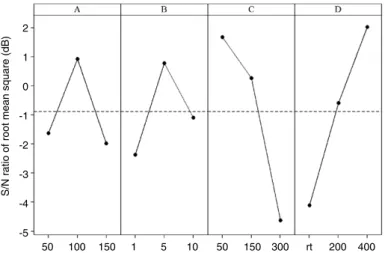
50 100 150 1 5 10 50 150 300 rt 200 400
S/N ratio of root mean square (dB)
2 1 0 -1 -2 -3 -4 -5
Fig. 1. S/N graph for RMS surface roughness of a ZnO buffer grown on glass. Note: A=rf power; B=Sputtering pressure;
C=Thickness; D=Post-annealing temperature.
contribution ratio. Additionally, post-annealing temperature also has some influence on the surface roughness, of about 37.29% in contribution ratio. The percent contribution of sputtering pressure and rf power to surface roughness was 9.91% and 9.84%, respectively.Fig. 1shows the S
/
N graph for the root mean square of ZnO buffer grown on glass. The S/
N graph is always ‘‘larger is better’’ and a positive number for S/
N is larger than negative number. As can be seen, the RMS surface roughness of the ZnO buffer surface decreases with a reduction in thickness. A similar behavior was observed20 25 30 35 40 45 50 55 60 65 70 75 2θ (degree)
Intensity (a.u.)
80
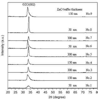
Fig. 2. XRD patterns of GZO films grown on a ZnO buffer for the L9orthogonal array from No. 1 to No. 9; in this case the
conditions for the deposition of the GZO films were fixed, while those for the ZnO buffer varied.
by Kim et al. [18]. Moreover,Fig. 1also reveals that the RMS surface roughness of the ZnO buffer decreases with an increase in post-annealing temperature. This is similar to the case of rf-deposited ZnO films [19].
3.2. Crystalline properties of GZO
GZO films having 600 nm thickness were grown (GZO/ZnO/glass) by maintaining the rf power at a constant value of 100 W and with the sputtering pressure at 0.67 Pa, as can be seen inTable 2.
Fig. 2shows the X-ray diffraction patterns of GZO films grown in all the already studied ZnO buffer layers (samples No. 1–No. 9 of the L9 orthogonal array). It is clear that for all GZO films only the (0 0 2) diffraction peak located at 2
θ ∼
34.
2°is observed, indicating that the films are polycrystalline with a hexagonal structure and a preferred orientation with the c-axis perpendicular to the substrate. These values are very close to those of the standard ZnO crystal (34.
45°). The crystalline quality of the ZnO films can be calculated by the intensity and full-width at half-maximum (FWHM) of the (0 0 2) peak [20]. FromFig. 2it is clear that the intensity of the GZO (0 0 2) diffraction is strongest for the ZnO buffer experimental conditions No. 8 (see conditions in table), indicating good crystalline quality for this sample. The grain size of the films from the XRD data is calculated using the Debye–Scherrer formula. The (0 0 2) peak position, FWHM value, and corresponding estimated grain size for ZnO buffer and GZO/ZnO/glass for all the L9orthogonal array are reported inTable 5. In a previous work by Moustaghfir et al. [21], they have also observed that the grain size of ZnO films increases with anneal-ing temperature. As can be seen, the ZnO buffer grain size increases from 10.78 to 25.04 nm. Moreover, the grain sizes of the ZnO buffer are estimated to be about 16.83, 16.08, and 25.04 nm, respectively, with a higher ZnO buffer annealing temperature (Table 5experimental conditions of Nos. 3, 4, and 8, respectively). A ZnO buffer of larger grain size yields GZO films also of larger grain size (Table 5. No. 8), indicating that the grain size of the GZO film is related to that the ZnO buffer [18]. The GZO film quality is strongly dependent on the ZnO buffer and the grain size in GZO films has a larger value.3.3. Optoelectronic properties of GZO
Comparing the results obtained using a ZnO buffer deposited under the experimental conditions of No. 8 (GZO/ZnO, A3B2C1D3/glass) and those obtained without a buffer (GZO/glass) shows that the
Table 5
X-ray results concerning (0 0 2) peak position, FWHM value and calculated grain size for all the ZnO buffer and GZO/ZnO/glass samples.
No. Control factors ZnO/glass GZO/ ZnO/glass
A B C D FWHM (°) 2θ(°) Grain size (nm) FWHM (°) 2θ(°) Grain size (nm)
1 1 1 1 1 0.80 33.91 10.39 1.01 34.90 8.25 2 1 2 2 2 0.77 33.75 10.79 0.98 34.25 8.49 3 1 3 3 3 0.49 34.10 16.97 0.63 34.48 13.21 4 2 1 2 3 0.52 34.15 15.99 0.61 34.70 13.65 5 2 2 3 1 0.57 34.15 14.59 0.58 34.85 14.37 6 2 3 1 2 0.63 33.89 13.19 0.77 34.35 10.81 7 3 1 3 2 0.53 33.95 15.68 0.56 34.95 14.88 8 3 2 1 3 0.33 34.20 25.21 0.53 34.05 15.69 9 3 3 2 1 0.49 34.21 16.98 0.81 34.26 10.27
Note: A=rf power; B=Sputtering pressure; C=ZnO buffer thickness; D=Post-annealing temperature.
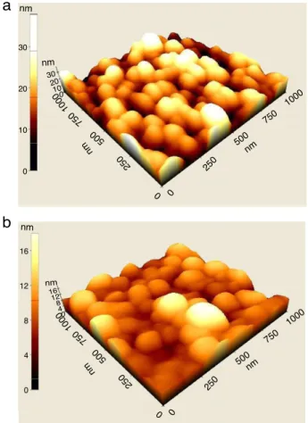
0 0 250 250 500 500 750 1000 nm nm nm nm 20 30 100 0 0 250 250 500 500 750 750 1000 1000 750 1000 nm nm nm 8 12 16 4 0 30 20 10 0 nm 16 12 4 0 8
a
b
Fig. 3. AFM images of GZO films on glass substrates (a) without buffer, Ra = 6.493 nm, (b) with the ZnO buffer and the
experimental conditions of No. 8, Ra=3.447 nm.
electrical resistivity decreases from 5
.
02×
10−3to 2.
94×
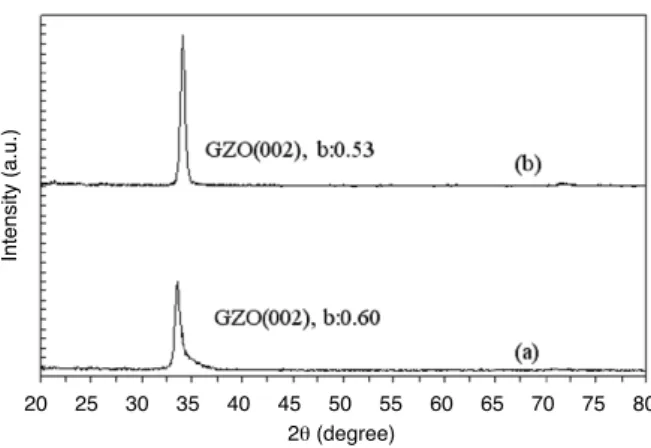
10−3cm while the optical transmittance in the visible region increases from 81.62% to 84.81%.Fig. 3shows the AFM images and RMS of GZO films on glass substrates with and without a buffer. As can be seen, the morphology of the GZO film with the ZnO buffer was slightly smoother compared to that without the ZnO buffer.Fig. 4shows the X-ray diffraction spectrum of GZO films when the ZnO buffer (experimental conditions of No. 8) was20 25 30 35 40 45 50 55 60 65 70 75 2θ (degree)
Intensity (a.u.)
80
Fig. 4. X-ray diffraction spectrum of GZO films on glass substrates (a) without buffer, grain size=13.88 nm, (b) with ZnO
buffer and the experimental conditions of No. 8, grain size=15.62 nm.
applied. As can be seen, the peak intensity of the (0 0 2) plane in the XRD patterns of the GZO film has the highest value. The grain sizes of GZO with and without the ZnO buffer are estimated to be about 15.62 nm and 13.88 nm, respectively.
Growth in grain size can reduce grain boundary scattering and increase carrier lifetime, thus leading to an increase in conductivity due to an increase in carrier concentration and Hall mobility [22]; as a result the electrical resistivity of GZO reduces. Furthermore, the larger grain size also leads to a decrease in surface roughness [23]. Low surface roughness can increase the GZO film transmittance, resulting in less light scattering.
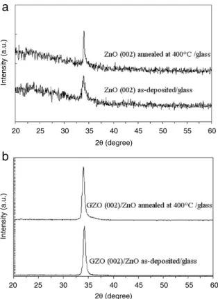
Fig. 5(a) shows the X-ray diffraction patterns of a ZnO/glass buffer, as-deposited and following annealing at 400°C, respectively. The ZnO/glass buffer has a fixed thickness of 50 nm, sputtering pressure of 0.67 Pa and rf power of 100 W. It is clear that the intensity of the X-ray peaks became sharpened and FWHM became narrower with the annealing treatment, which means that this treatment leads to an improvement in the crystallinity of the ZnO/glass buffer.Fig. 5(b) shows the XRD patterns of the GZO/ZnO/glass structure, where the intensity of the (0 0 2) diffraction peak becomes stronger by applying an annealed treatment ZnO/glass buffer, indicating that the crystalline quality of the GZO film is improved.
To study the crystalline quality of GZO films deposited on ZnO buffer layers of various thicknesses, three new buffer samples with thicknesses of 50, 150, and 300 nm were produced at a sputtering pressure of 0.67 Pa and rf power of 100 W. All the samples were then annealed in vacuum at 400°C before the growth of the GZO film.Fig. 6shows the corresponding X-ray spectrum. It can be seen that GZO films deposited on a 50-nm thick ZnO buffer layer exhibit both the strongest intensity of (0 0 2) diffraction and the smallest full-width at half-maximum (FWHM) value, indicating a good crystalline quality. Optical and electrical studies of the GZO sample grown on the annealed 50-nm thick ZnO buffer show that the electrical resistivity of GZO was very low (2
.
94×
10−3cm) and the transmittance was very high (84.81% in the visible region).3.4. Optimal deposition parameters
The data sequences of the ‘lower-the-better’ performance characteristic for the electrical resistivity and the ‘higher-the-better’ performance characteristic for the optical transmittance were pre-processed as follows [24,25]: x∗i
(
k)
H=
x0i(
k) −
min x0i(
k)
max x0i(
k) −
min x0i(
k)
k=
1∼
n,
i=
1∼
9 (4) x∗i(
k)
L=
max x0i(
k) −
x0i(
k)
max x0i(
k) −
min x0i(
k)
k=
1∼
n,
i=
1∼
9 (5)20 25 30 35 40 45 50 55 60 2θ (degree) Intensity (a.u.) 20 25 30 35 40 45 50 55 60 2θ (degree) Intensity (a.u.)
a
b
Fig. 5. X-ray diffraction patterns of ZnO as-deposited and following annealing in vacuum at 400°C; (a) ZnO/glass, (b)
GZO/ZnO/glass. ZnO buffer at a fixed thickness of 50 nm, sputtering pressure of 0.67 Pa, and rf power of 100 W.
20 25 30 35 40 45 50 55 60
2θ (degree)
Intensity (a.u.)
Fig. 6. X-ray diffraction patterns of GZO films deposited on different ZnO buffer thicknesses, (a) 50 nm, (b) 150 nm, and (c) 300
nm. ZnO buffer at a fixed sputtering pressure of 0.67 Pa, rf power of 100 W, and annealed in vacuum at 400°C (b: full width at
half maximum).
where n is the performance characteristic and i is the experimental number, x∗
i
(
k)
H and x∗i(
k)
Lare the ‘higher-the-better’ and ‘lower-the-better’ values after grey relational generation, respectively; min x0Table 6
Grey relational grade and orders.
Experiment No. Process parameter Grey relational grade Order
A B C D 1 1 1 1 1 0.468 8 2 1 2 2 2 0.664 3 3 1 3 3 3 0.514 7 4 2 1 2 3 0.862 2 5 2 2 3 1 0.644 4 6 2 3 1 2 0.561 6 7 3 1 3 2 0.586 5 8 3 2 1 3 0.957 1 9 3 3 2 1 0.431 9 Table 7
Results of ANOVA for the grey relational grade in the GZO grown on ZnO/glass.
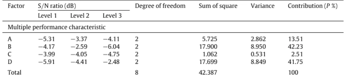
Factor S/N ratio (dB) Degree of freedom Sum of square Variance Contribution (P %)
Level 1 Level 2 Level 3
Multiple performance characteristic
A −5.31 −3.37 −4.11 2 5.725 2.862 13.51
B −4.17 −2.59 −6.04 2 17.900 8.950 42.23
C −3.99 −4.05 −4.75 2 1.062 0.531 2.51
D −5.91 −4.41 −2.48 2 17.699 8.849 41.75
Total 8 42.387 100
coefficient
ξ
i(
k)
can be calculated as follows:ξ
i(
k) =
∆min
+
ς
∆max∆0i
(
k) + ς
∆max(6) where x∗
0
(
k)
is the reference sequence, x∗
j
(
k)
is the comparability sequence,ς
is the distinguishing coefficient,ς ∈
[0,
1]. The value ofς
can be adjusted according to the actual system requirement withς =
0.
5 selected in this study.∆0i=
x∗0(
k) −
x∗i(
k)
is the difference in absolute value between x∗0
(
k)
and x∗
i
(
k)
; ∆min=
min∀j∈imin∀k
x∗0(
k) −
xj∗(
k)
is the smallest value of∆0iand∆max
=
max∀j∈imax∀k
x∗0(
k) −
xj∗(
k)
is the largest value of∆0i.The grey relational grade
(γ
i)
is a weighted sum of the grey relational coefficient. It is defined as follows:γ
i=
1 n n−
k=1ξ
i(
k).
(7)The experimental data of the multi-response characteristics are evaluated using this grey relational grade. The evaluated grey relational grade fluctuates from 0 to 1 and equals 1 if these two sequences are identically coincident. The optimum level of the process parameters is the level with the highest grey relational grade.
The grey relational grade for each experiment using the L9orthogonal array is shown inTable 6. A higher grey relational grade represents that the corresponding experimental result is closer to the ideal normalized value. In other words, the larger the grey relational grade, the better will be the multiple performance characteristics. Since (A3B2C1D3) has the highest grey relational grade (experimental conditions of No. 8), it has the best multiple performance characteristics among all experiments.Table 7lists the results of the ANOVA for the grey relational grade in the GZO grown on ZnO/glass. As can be seen, the main contribution percentages for sputtering pressure (B) and post-annealing temperature (D) to multiple performance characteristics were 42.23% and 41.75%, respectively.
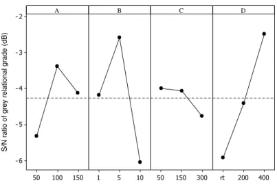
Fig. 7shows the graph of the grey relational grade for each deposition parameter at different levels. FromFig. 7, the optimum buffer conditions to obtain good multiple performance characteristics in the
Fig. 7. The S/N graph for the grey relational grade. Table 8
Confirmation test results for multiple performance characteristics with initial and optimal process parameters.
Initial process parameters(A3B2C1D3)
Resistivity: 2.94×10⁻³cm
Transmittance: 84.81%
The full width at half maximum of XRD: 0.53°
Optimal process parameters(A2B2C1D3)
Resistivity: 9.44×10⁻⁴cm
Transmittance: 85.82%
The full width at half maximum of XRD: 0.47°
GZO grown on ZnO/glass are given by the combination A2B2C1D3; this means 100 W rf power, 0.67 Pa, 50 nm thickness, and annealing temperature at 400°C. A comparison of the confirmed experimental results using the initial and optimal deposition parameters is shown inTable 8, and it is evident that the multiple performance characteristics of GZO films can be improved by the grey-Taguchi method. Applying grey theory prediction design (A2B2C1D3) led to a decrease in full width at half maximum (FWHM, reduced from 0
.
53°to 0.
47°for GZO films), meaning that an improvement in the crystallinity and a larger crystallite size of the films can be obtained. The resistivity decreased from 2.
94×
10−3to 9.
44×
10−4cm; the optical transmittance was improved slightly (increased from 84.81% to 85.82%) for GZO films.4. Conclusions
Ga2O3-doped ZnO films and ZnO buffer were deposited on glass substrates by rf magnetron sputtering. A grey-Taguchi method was established to combine grey relational analysis and the Taguchi method. This paper has discussed an application of the L9mixed orthogonal array in the Taguchi quality design of a ZnO buffer in the deposition of GZO transparent conductive films. The influence of various deposition conditions of the ZnO buffer layer on the structure, surface roughness, and optoelectronic properties of GZO films were studied. The RMS surface roughness of the ZnO buffer decreases with an increase in the post-annealing temperature and a reduction in thickness. The XRD diffraction pattern shows that the GZO films are polycrystalline with a hexagonal structure and a preferred orientation with a c-axis which is perpendicular to the substrate surface. The ANOVA results for the grey relational grade in the GZO grown on ZnO/glass indicate that ZnO sputtering pressure and ZnO post-annealing temperature significantly affect the electrical resistivity and optical transmittance of the GZO films. In the confirmation runs, it is clearly shown that multiple performance characteristics can be improved by using the grey-Taguchi method.
References
[1] T. Minami, T. Yamamoto, T. Miyata, Thin Solid Films 366 (2000) 63. [2] K.H. Bang, D.K. Hwang, J.M. Myoung, Appl. Surf. Sci. 207 (2003) 359. [3] K.Y. Cheong, Norani Muti, S. Roy Ramanan, Thin Solid Films 410 (2002) 142. [4] H. G’omez, M. de la, L. Olvera, Mater. Sci. Engng. B 134 (2006) 20.
[5] V. Khranovskyy, U. Grossner, O. Nilsen, V. Lazorenko, G.V. Lashkarev, B.G. Svensson, R. Yakimova, Thin Solid Films 515 (2006) 472.
[6] C.Y. Hsu, T.F. Ko, Y.M. Huang, J. European Ceramic Society 28 (2008) 3065.
[7] K. Haga, T. Suzuki, Y. Kashiwaba, H. Watanabe, B.P. Zhang, Y. Segawa, Thin Solid Films 433 (1–2) (2003) 131. [8] T. Yamamoto, T. Sakemi, K. Awai, S. Shirakata, Thin Solid Films 451–452 (2004) 439.
[9] H. Gomez, A. Maldonado, M. de la, L. Olvera, D.R. Acosta, Sol. Energy Mater. Sol. Cells 87 (2005) 107. [10] S.M. Park, T. Ikegami, K. Ebihara, Thin Solid Films 513 (2006) 90.
[11] Y.S. Tarng, S.C. Juang, C.H. Chang, J. Mate. Proc. Tech. 128 (2002) 1. [12] C.Y. Hsu, C.K. Huang, C.Y. Wu, Int. J. Adv. Manuf. Tech. 34 (2007) 857. [13] D.Y. Chen, C.Y. Hsu, Superlattices Microstruct. 44 (2008) 742.
[14] J.Z. Zhang, J.C. Chen, E.D. Kirby, J. Mater. Process. Technol. 184 (2007) 233. [15] C.Y. Hsu, C.H. Tsang, Sol. Energy Mater. Sol. Cells 92 (2008) 530. [16] S.J. Kim, K.S. Kim, H. Jang, J. Mater. Proc. Tech. 136 (2003) 202.
[17] S. Flickyngerova, K. Shtereva, V. Stenova, D. Hasko, I. Novotny, V. Tvarozek, P. Sutta, E. Vavrinsky, Appl. Surf. Sci. 254 (2008) 3643.
[18] H.W. Kim, N.H. Kim, Appl. Surf. Sci. 236 (2004) 192.
[19] S.Y. Chu, W. Water, J.T. Liaw, J. Euro. Cera. Soci. 23 (2003) 1593.
[20] Z.B. Fang, Z.J. Yan, Y.S. Tan, X.Q. Liu, Y.Y. Wang, Appl. Surf. Sci. 241 (2005) 303.
[21] A. Moustaghfir, E. Tomasella, S. Ben Amor, M. Jacquet, J. Cellier, T. Sauvage, Surf. Coat. Tech. 174/175 (2003) 193. [22] M. Lv, X. Xiu, Z. Pang, Y. Dai, S. Han, Appl. Surf. Sci. 252 (2005) 2006.
[23] H. Ko, W.P. Tai, K.C. Kim, S.H. Kim, S.J. Suh, Y.S. Kim, J. Crystal Growth 277 (2005) 352. [24] B.M. Gopalsamy, B. Mondal, S. Ghosh, Int. J. Adv. Manuf. Technol. 45 (2009) 1068. [25] J.L. Deng, The Essential Method of Grey Systems, HUST Press, Wuhan, China, 1992.