Growth of semi-polar GaN-based light-emitting diodes grown on an
patterned Si substrate
Ching-Hsueh Chiua, Da-Wei Lina, Zhen-Yu Lia, Shih-Chun Ling a,b, Hao-Chung Kuoa , Tien-Chang Lua, Shing-Chung Wanga, Wei-Tasi Liaob, Tomoyuki Tanikawac, Yoshio Hondac, Masahito Yamaguchic, Nobuhiko Sawakid
aDepartment of Photonics & Institute of Electro-Optical Engineering, National Chiao Tung
University, 1001 Ta Hsueh Road, Hsinchu 30010, Taiwan
bDepartment of Opto-Electronics Epitaxy and Devices, Industrial Technology Research Institute,
Rm. 206, Bldg 78, 195, Sec. 4, Chung Hsing Rd., Chutung, Hsinchu 31040, Taiwan
cDepartment of Electronics, Nagoya University, 3C-1, Furo-cho, Chikusa, Nagoya, Aichi, 464-8603,
Japan
dDepartment of Electrical & Electronic Engineering, Aichi Institute of Technology, 1247 Yachigusa,
Yakusa, Toyota 470-0392, Japan
1. Abstract:
We present a study of semi-polar (11¯01) InGaN-based light emitting diodes (LEDs) grown on patterned (001) Si substrates by atmospheric-pressure metal organic chemical vapor deposition. A transmission electron microscopy image of the semi-polar template shows that the threading dislocation density was decreased significantly. From electroluminescence measurement, semi-polar LEDs exhibit little blue-shift and low efficiency droop at a high injection current because the reduction of the polarization field not only made the band diagram smoother but also restricted electron overflow to the p-GaN layer as shown in simulations. These results indicate that semi-polar InGaN-based LEDs can possess a high radiative recombination rate and low efficiency droop at a high injection current.
Keywords: LEDs, MOCVD, Si, semi-polar, efficiency droop
2. Introduction:
In the past two decades, GaN-based photoelectronic devices have drawn tremendous attention due to their potential to replace incandescent lamps and greatly promote energy conversion efficiency1). Most of the devices developed to date were grown on sapphire or SiC substrates, and usually the GaN epitaxal films have a high threading dislocation density (TDD). Thus, several methods have been applied to reduce the impact of the TDD. For example, epitaxial lateral overgrowth (ELO) by using the selective area growth technique (SAG) is effective in reducing the TDD2). On the other hand, the low thermal and electrical conductivities make sapphire less suitable as a substrate for GaN epilayers. Nevertheless, sapphire still has a low cost of production, and it is the most widely used substrate material. While the high price and some mechanical defects reduce the acceptability of SiC substrates in the light- emitting diodes (LEDs), silicon has been considered as an alternative substrate due to its low manufacturing cost, large size, and good thermal and electrical conductivities3).
from the quantum-confined Stark effect (QCSE) as a result of a spontaneous and piezoelectric polarization field parallel to the [0001] direction4). This effect reduces the oscillator strength, restricts the carrier recombination efficiency, and induces a red shift in photon emission. In order to reduce the polarization field, a device fabricated on semi-polar or non polar surface has been proposed5-6). Following a similar thought, researches at Nagoya University demonstrated that by using a SiO2 nanomask and SAG, a semi-polar GaN film with high quality can be grown on a Si
substrate7-9), and great progress has been made in terms of reducing the TDD in GaN grown on a Si substrate. In this paper, InGaN-based LED structures grown on semi-polar (11¯01) GaN films are investigated and compared with InGaN based LED structures grown on (0001) GaN/(111) Si. From electroluminescence (EL) measurement, semi-polar LEDs exhibit a smaller blue shift of the wavelength peak and lower efficiency droop at a high injection current. To examine the physical origin of efficiency droop in InGaN/GaN LEDs, we also performed a theoretical calculation based on the aforementioned polar c-plane and semi-polar LED structures using semiconductor device simulation software (APSYS).
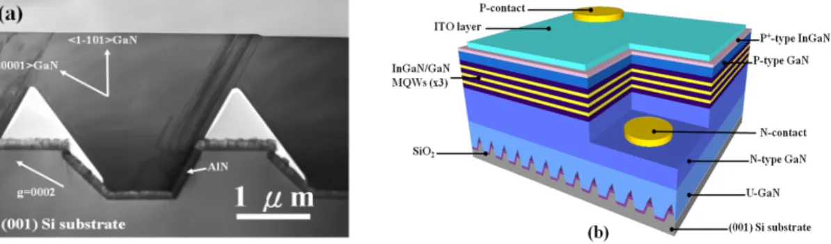
The epitaxial structure for InGaN-based LEDs on semi-polar (11¯01) GaN films was prepared as follows. First, a semi-polar (11¯01) undoped GaN (u-GaN) film was grown on a 7。 off-oriented
n-type (001) silicon substrate by atmospheric-permanent hyphen pressure metal organic chemical vapor deposition (AP-MOCVD), and the related processes have been reported in our previous study8). A transmission electron microscopy (TEM) image of the semi-polar (11¯01) GaN template is shown in Fig. 1(a). As we can see, most of the threading dislocations generated near the AlN buffer layer/Si interface turn to the direction perpendicular to (0001) and are soon terminated. As a result, we can achieve a low TDD in the top (11¯01) GaN layer as the growth proceeds. Next, we deposited the InGaN-based LED structure on this semi-polar GaN template by AP-MOCVD as depicted in Fig. 1(b). The epitaxial structure starts with 0.5 μm n-doped GaN (n-GaN), 3 pairs of multi-quantum wells (4 nm InGaN wells and 8 nm GaN barriers), and 0.2 μm p-doped GaN (p-GaN). Finally, we grew a 0.2 nm heavily p-doped InGaN (p-InGaN) contact layer. The Ni/Au (5/5 nm) and AuSb (200 nm) were used as p-type and n-type contacts to the diode, respectively.
Fig.1 (a) The TEM of semi-polar (11¯01) GaN template. (b) Schematic of GaN-based LED structure semi-polar (11¯01) GaN template.
3. Result and discussion:
Fig. 2 shows the EL spectra of the device measured at various dc currents. The emission peak wavelength of the semi-polar LEDs is slightly blue-shifted (about 1.7 nm) compared with that
of c-plane LEDs (about 3.5 nm). This means that the InGaN- based LEDs on the (11¯01) GaN/7。
off-axis (001) Si substrates have a very low internal piezoelectric field, and this phenomenon leads to the decrease of the QCSE10). Fig. 3 shows normalized external quantum efficiency (EQE) as a function of forward current density for c-plane LEDs and semi-polar LEDs. For the c-plane LEDs, when the current density exceeds 60 A/cm2, the EQE is reduced to 57% of its maximum value. In contrast, the semi-polar LEDs exhibit only 10% efficiency droop when increasing the injection current density to 60 A/cm2.The reduction of efficiency droop is quite clear. In order to explore the physical origin of efficiency droop in InGaN/GaN LEDs, we performed a simulation of the above polar c-plane and semi-polar LED structures using the APSYS simulation software11). Commonly accepted parameters are used in the simulations, including a Shockley-Read-Hall recombination lifetime of 4 ns and an Auger recombination coefficient of 6×10-30 cm6s-1. The results of the EQE droop simulation of both different polar LED structures are in good agreement with the experimental data as shown in Fig. 3.
Fig.2 EL spectra of semi-polar LEDs at different drive currents. The inserts show the EL peak wavelength as a function of the drive current.
Fig.3 Experimental and simulated EQE as a function of forward current density for c-plane LEDs and semi-polar LEDs.
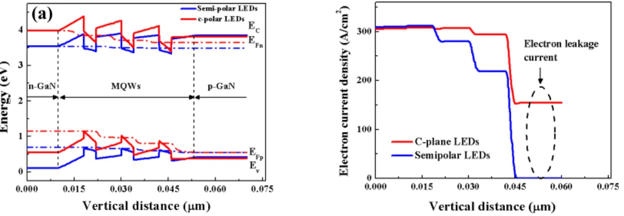
Furthermore, to reveal the physical situation behind our results, we have to check the actual band diagram and the carrier distribution in our simulation. Fig. 4(a) shows the calculated energy band diagram of reference c-plane and semi-polar LEDs at a forward current 60 mA. As we can see in the plot, the band diagram of c-plane LEDs is severely bent, which results from the polarization
charge. Besides, we observed the upward conduction band edge while it approaches the multi quantum well (MQW) region from the n-GaN side, and the conduction band near n-GaN is higher than the conduction band near p-GaN, which results in a large electron leakage current as shown in Fig. 4(b). We have to keep in mind that the electrons that escaped from the MQW active region do not contribute to radiative recombination and deteriorate the LED efficiency at a high injection current. A previous report indicated that the electron leakage current due to a polarization field is one of the dominant mechanisms that cause efficiency droop12). In the semi-polar LEDs, due to the reduction of the polarization field, the conduction band on the p-GaN side is higher than the conduction band on the n-GaN side. This results in much less electron leakage in the semi-polar case.
Fig.4 (a) Calculated band diagram of c-plane LEDs and semi-polar LEDs under forward bias operation. (b) Simulated electron current density for c-plane LEDs and semi-polar LEDs at 60 mA forward current.
Fig. 5 shows the calculated carrier distribution in the InGaN/GaN MQW structure at a forward current of 60 mA for c-plane LEDs and semi-polar LEDs. We notice that the carrier distribution among quantum wells varies a lot in the c-plane case, but not in the semi-polar case. Comparing electrons and holes, holes suffer more as a result of this nonuniformity due to their large effective mass and low mobility. Also the relative locations of distributions of electrons and holes matched quite well in the semi-polar sample as shown in Fig. 5(b), which can directly promote the radiative recombination rate. Thus, the much reduced polarization field in the semi-polar sample can reduce the carrier leakage and increase electron-hole pair radiative recombination simultaneously.
Fig.5 Distribution of carrier concentration of InGaN/GaN MQWs structure at 60 mA forward current density for (a) c-plane LEDs and (b) semi-polar LEDs.
4. Conclusion:
In summary, we present a study of a structure grown on semi-polar (11¯01) InGaN/GaN LEDs, which had been grown on patterned (001) Si substrates by AP-MOCVD. The TEM image of the semi-polar template shows was decreased significantly. In addition, a small blue shifted of the EL emission peak wavelength and low efficiency droop in semi-polar (11¯01) InGaN/GaN LEDs are clearly observed. Our theoretical simulations indicate that the reduction of the polarization field in the semi-polar MQW active region leads to the uniform distribution of holes and decreases the electron leakage, which result in a significant reduction of efficiency droop.
Acknowledgments
The authors are grateful to the National Science Council of the Republic of China, Taiwan, for financially supporting this research under Contract No. NSC 98-2923-E-009-001-MY3.
References
[1]David L. Evans: Proc. SPIE. 3002 (1997) 142.[2]N. P. Kobayashi, J. T. Kobayashi, X. Zhang, P. D. Dapkus, and D. H. Rich: Appl. Phys. Lett. 74 (1999) 2836.
[3]Baoshun Zhang, Hu Liang, Yong Wang, Zhihong Feng, Kar Wei Ng, and Kei May Lau: J. Cryst. Growth 298 (2007) 725.
[4]T. Takeuhi, H. Amano, and I. Akasaki: Jpn. J. Appl. Phys. 39 (2000) 413.
[5]R. Sharma, P. M. Pattison, H. Masui, R. M. Farrell, T. J. Baker, B. A. Haskell, F. Wu, S. P. DenBaars, J. S. Speck, and S. Nakamura: Appl. Phys. Lett. 87 (2005) 231110.
[6]A. Chakraborty, B. A. Haskell, S. Keller, J. S. Speck, S. P. DenBaars, S. Nakamura, and U. K. Mishra: Appl. Phys. Lett. 85 (2004) 5143.
[7]Shigeyasu Tanaka, Yasutoshi Kawaguchi, and Nobuhiko Sawaki, Michio Hibino and Kazumasa Hiramatsu: Appl. Phys. Lett. 76 (2000) 2701.
[8]Y. Honda, N. Kameshiro, M. Yamaguchi, and N. Sawaki: J. Cryst. Growth 242 (2002) 82. [9]Nobuhiko Sawaki, Toshiki Hikosaka, Norikatsu Koide, Shigeyasu Tanaka, Yoshio Honda, and Masahito Yamaguchi: J. Cryst. Growth 311 (2009) 2867.
[10]Yoshio Honda, Norifumi Kameshiro, Masahito Yamaguchi, Nobuhiko Sawaki: J. Cryst. Growth 242 (2002) 82.
[11]Hongbo Yu, L. K. Lee, Taeil Jung, and P. C. Ku: Appl. Phys. Lett. 90 (2007) 141906. [12]APSYS by Crosslight Software Inc, Burnaby, Canada: http://www.crosslight.com
[13]Shih-Chun Ling, Tien-Chang Lu, Shih-Pang Chang, Jun-Rong Chen, Hao-Chung Kuo, and S hing-Chung Wang: Appl. Phys. Lett. 96 (2010) 231101.