Effect of Bottom Electrode Materials and Annealing Treatments on the
Electrical Characteristics of Ba
0.47Sr
0.53TiO
3Film Capacitors
Ming-Shiahn Tsai, Shi-Chung Sun,
†and Tseung-Yuen Tseng
*Department of Electronics Engineering and Institute of Electronics, National Chiao Tung University, Hsinchu 30050, Taiwan, Republic of China The dielectric constant and leakage current density of
Ba0.47Sr0.53TiO3 (BST) thin films deposited by radio-frequency magnetron sputtering on various bottom elec-trode materials (Pt, Ir, IrO2/Ir, Ru, RuO2/Ru) before and after annealing in O2 and N2 ambient were investigated. Improvement in crystallinity of BST films deposited on various bottom electrodes was observed with annealing. The refractive index, dielectric constant, loss tangent, and leakage current of the films were also strongly dependent on annealing conditions. A BST thin film deposited on an Ir bottom electrode at 500°C, after 700°C annealing in O2for 20 min, had a dielectric constant of 593 ± 5%, a loss tan-gent of 0.019 ± 10% at 100 kHz, a leakage current of (2.1 ± 13%) × 10−8A/cm2at an electric field of 100 kV/cm with a delay time of 30 s, and a charge storage density of 53 ± 5% fC/µm2 at an applied field of 150 kV/cm. Based on the dielectric constant, leakage current, and reliability, the op-timum material for the bottom electrode with annealing was Ir. Interdiffusion of Ru and Ti at the interface between the BST film and Ru electrode was observed in 500°–700°C annealed samples. The 10 year lifetime of time-dependent dielectric breakdown (TDDB) studies indicated that BST on Pt, Ir, IrO2/Ir, Ru, and RuO2/Ru had long lifetime over 10 years of operation at a voltage bias of 1 V.
I. Introduction
T
HINfilms with high dielectric constant have attracted great attention in recent years for use as cell capacitors for high-density dynamic random access memories (DRAMs). These films can lower the height of the storage node and simplify the cell structure.1–5(Ba,Sr)TiO3films have been reported to be
the most promising capacitor materials for gigabit DRAMs because of their high dielectric constant, low leakage current density, high dielectric breakdown strength, paraelectric perovskite phase (that does not exhibit fatigue), aging, and ease of composition control.1–9
The electrical characteristics of (Ba,Sr)TiO3 thin films
greatly depend on deposition conditions (sputtering power, substrate temperature, sputtering ambient, gas pressure, etc.),6,9–11composition of the BST thin films,3,12bottom
elec-trode material (e.g., Pt, Pt/Ta, Pt/TiN/Ti, Pd/Ti, Pd, etc.),13–15
and postannealing conditions.10,16–18Although there is much
experimental proof that annealing conditions can significantly affect the properties of the films, systematic studies of the effect of annealing conditions on the dielectric and electrical
properties of (Ba,Sr)TiO3 thin films on various bottom
elec-trodes are still quite limited. In the practical process of fabri-cating semiconductor devices, several annealing processes, such as the annealing of Al in forming gas (N2/H2⳱ 95/5) at
400°C and flow of boron phosphosilicate glass films in N2(at
∼800°C), have been used after the deposition of (Ba,Sr)TiO3
thin films.19Therefore, stability in various ambients, a good
diffusion barrier, and good adhesion to the surfaces encoun-tered in microelectronics are major requirements. In Refs. 20 and 21, we have studied the effects of bottom electrode mate-rials (Pt, Ir, IrO2/Ir, Ru, RuO2/Ru) on the dielectric constant
and leakage current density in Ba0.47Sr0.53TiO3 (BST) thin
films and proposed them as optimum electrode materials. The structure and the electrical and dielectric properties of the films were evaluated and discussed.
The present work attempts to more thoroughly understand the effects of annealing on the dielectric constant and leakage current density in BST thin films grown on various bottom electrodes (Pt, Ir, IrO2/Ir, Ru, RuO2/Ru). The structure and the
electrical and dielectric properties of the films are characterized and discussed.
II. Experimental Procedures
BST thin films were deposited on metal/SiO2/(100)Si (metal⳱
Pt, Ir, IrO2/Ir, Ru, and RuO2/Ru) bottom storage node
elec-trodes by radio-frequency (rf ) magnetron sputtering. Metal lay-ers 100 nm thick were deposited on SiO2/Si substrate using a
separate rf magnetron sputtering system. The detailed deposi-tion condideposi-tions of the BST thin films on various bottom elec-trodes were described in Ref. 20.
Unless otherwise mentioned, BST films ∼100 and 80 nm thick were deposited at substrate temperatures of 27° and 500°C. After deposition, the BST thin films were annealed for 20–30 min at 500°–750°C in O2, N2, or pure N2O atmosphere
using a quartz-glass tube furnace (FN) and rapid thermal anneal (RTA) for 1–3 min at a heating rate of 100°C/s and cooling rate of 5°C/s. Finally, the 50 nm thick top Pt electrodes with diam-eters of 165, 255, and 350m were formed by sputtering and then patterned by the shadow mask process.
Film thickness was determined by ellipsometry. The struc-ture was characterized by X-ray diffraction (XRD; Model D5000, Siemens, Karlsruhe, Germany). The chemical compo-sition of the films (Ba/Sr ⳱ 47/53) was close to the target composition (Ba/Sr⳱ 50/50) within a deviation of 3% on the basis of the measured results of inductively coupled plasma atomic emission spectrometry (ICP-AES; Model SCIEX ELAN 5000, Perkin Elmer, Norwalk, CT) method. Surface roughness and morphology were examined by atomic force microscopy (AFM; Nano-Scope III, Digital Instruments, To-nawanda, NY). Depth profile analysis of deposited films was performed with secondary ion mass spectrometry (SIMS; Model IMS-4f, Cameca, Courbevoı´e, France) with primary ion of Cs+and sputtering rate of 0.5 nm/s. The capacitance–voltage
(c–v) characteristic was measured on the metal–insulator– metal (MIM) structure by measuring capacitance at 100 kHz as a function of swept positive-to-negative voltage bias. The di-B. A. Tuttle—contributing editor
Manuscript No. 190919. Received June 17, 1997; approved May 26, 1998. Supported by the National Science Council of R.O.C. under Project No. NSC 85-2112-M009-037.
*Member, American Ceramic Society.
†Also with Taiwan Semiconductor Manufacturing Co., Ltd., Hsinchu, Taiwan.
Journal
electric constant of the films was calculated from capacitance measured at 100 kHz without bias voltage. Dielectric and loss properties were measured as a function of frequency with an impedance gain phase analyzer (Model HP4194A, Hewlett-Packard, Palo Alto, CA). Current–voltage (I–V) measurements were performed by measuring the current through the sample with a semiconductor parameter analyzer (Model HP4145B, Hewlett-Packard). A Pt top electrode of the BST capacitor was connected to the voltage source, and the bottom electrode was grounded. Polarity was positive when positive voltage was ap-plied to the top electrode. Time-dependent dielectric break-down (TDDB) measurements were performed by measuring the current–time (I–t) with constant voltage through the sample with the HP4145B semiconductor parameter analyzer. Experi-mental data reported in this paper represent multiple measure-ments on ten specimens.
III. Results and Discussion
Figure 1 shows the XRD patterns of BST thin films depos-ited on Pt bottom electrodes at 27°C and subsequently annealed for 30 min and 1 or 3 min at 750°C in O2and N2ambient. The
(110) and (200) peak intensities of the BST thin films increase with increasing annealing time in O2 and N2 ambient. The
(110) peak intensity of the films after O2annealing for 30 min
has 3 times the intensity of that of films annealed for 3 and 1 min. All the annealed BST films are slightly crystallized. Fig-ure 2 illustrates XRD patterns of 80 nm thick BST thin films deposited on Pt, Ir, IrO2/Ir, Ru, and RuO2/Ru bottom electrode
materials at 500°C. The as-deposited films on Pt, Ir, and Ru show that the BST film on Ru has the stronger (110) peak and that on Pt has the weaker (110) peak. BST films deposited on Ir and Ru show stronger (110) peaks than those on IrO2/Ir and
RuO2/Ru, respectively. A stronger and sharper perovskite
(110) peak from the film deposited on Ru compared to those from the films deposited on other bottom electrodes implies an improved crystallinity and is obtained in the film on Ru. The (101) peak of RuO2is observed in BST on Ru, and, therefore,
a thin RuO2layer can be formed at the interface between BST
and Ru during deposition. Figures 3(a) and (b) show XRD patterns of 80 mm thick BST thin films deposited on Pt and Ir at 500°C and subsequently furnace (FN) annealed at 500°, 600°, and 700°C in O2ambient for 20 min. The results of these
figures indicate that the (110), (100), and (200) diffraction
peaks of BST films on Pt and Ir increase with increasing an-nealing temperature. Figure 3(c) shows the XRD patterns of 80 nm thick BST thin films deposited on Ru bottom electrode at 500°C and subsequently annealed under the same conditions as those in Figs. 3(a) and (b). The (111) and (100) diffraction peaks of the BST films on Ru increase with increasing anneal-ing temperature (Fig. 3(c)). The RuO2 (101) peaks of BST
films on Ru increase as annealing temperature increases, indi-cating that more RuO2is formed at the interface between BST
and Ru during annealing. XRD results suggest that improve-ment in the crystallinity of BST films can be achieved by annealing treatments.
Figure 4 shows that the thicknesses of BST thin films de-posited on Pt at 27°C and subsequently annealed at 550°, 650°, or 750°C in N2 ambient vary with annealing time. The
thick-nesses of BST films annealed at 550° and 650°C decrease with increasing annealing time. And the thickness of 750°C-annealed BST film also decreases with increasing annealing time, but it attains saturation when annealed over 1 min. XRD results suggest that, after annealing, improvement in crystal-linity of the films is not observed in the 550°C-annealed film. But crystallinity of the 650°- and 750°C-annealed films is slightly improved. The thickness reductions of the films can be explained as a result of an increase in density and the elimi-nation of porosity.
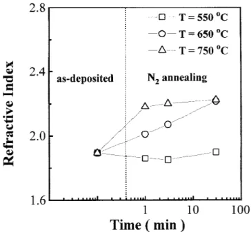
Figure 5 depicts the change in refractive index of BST thin films deposited on Pt at 27°C and subsequently annealed for 30 min and 1 or 3 min at 550°, 650°, and 750°C in N2 ambient
with annealing time. The refractive index for the BST annealed at 550°C approaches a constant value of 1.85, which is close to 1.8, the index of refraction of sputter-deposited amorphous BST.18,22,23 The refractive indexes of the 650°- and
750°C-annealed BST increase with increasing annealing time and in-crease to 2.2, which approaches the refractive index (2.3) of microcrystalline BST films.18,22,23 (The refractive index was
previously shown to be affected by composition.24) An ICP
study indicates that annealing-induced composition change in the films is not observed as long as the annealing temperature remains <750°C. Therefore, the change in the refractive index can be interpreted only as a pure annealing effect.24 An
in-crease in the index of refraction is usually attributed to either densification or crystallization. Densification is observed in the 550°C annealed sample (Fig. 4), but its refractive index ap-proaches a constant value of 1.85. Slight crystallization is ob-served in the 650° and 750°C-annealed samples but not in the
Fig. 1. XRD patterns of BST films deposited at 27°C on Pt and subsequently annealed for 30 min and 1 or 3 min at 750°C in O2and N2ambient.
Fig. 2. XRD patterns of BST films deposited at 500°C on Pt, Ir, IrO2/Ir, Ru, and RuO2/Ru bottom electrodes.
550°C annealed sample, based on XRD results (not shown here). In fact, both 650° and 750°C annealed samples can achieve the same refractive index of 2.2 after 30 min annealing. Therefore, the change in the index of refraction is believed to correlate with the increased crystallization of the films.
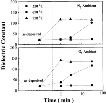
Figure 6 shows that the dielectric constant of BST thin films annealed at different temperatures varies with annealing time. The dielectric constant of BST annealed at 550°C in N2or O2
ambient does not change with annealing time and approaches a constant value∼23, because its crystallinity is not improved by annealing (on the basis of XRD results). The dielectric con-stants of BST annealed at 650° and 750°C increase with in-creasing annealing time, which is attributed to the inin-creasing crystallization of the films. The dielectric constant and refrac-tive index of BST films vary with annealing temperature and behave similarly, as indicated in Figs. 5 and 6.
Fig. 5. Refractive index of BST films deposited at 27°C on Pt and subsequently annealed for 30 min and 1 or 3 min at 550°, 650°, and 750°C in N2ambient.
Fig. 3. XRD patterns of BST films deposited at 500°C on (a) Pt, (b) Ir, and (c) Ru and subsequently annealed for 20 min at 500°, 600°, and 700°C in O2ambient.
Fig. 4. Film thickness of BST films deposited at 27°C on Pt and subsequently annealed for 30 min and 1 or 3 min at 550°, 650°, and 750°C in N2ambient.
Figure 7 shows that leakage current at 100 kV/cm with a delay time of 30 s (a transient leakage current) for BST thin films, which are deposited and annealed under the same con-ditions as those in Fig. 6 before top-electrode deposition, is dependent on annealing time and temperature. The leakage current of BST annealed at 550°C decreases with increasing annealing time because of increasing densification of BST films after annealing, as shown in Fig. 4. The leakage current of BST annealed at 750°C increases with increasing annealing time, because the increase in the dielectric constant of 750°C annealed film (Fig. 6) can be due to the enhanced ionic polar-ization and improved crystallinity with larger grain size.
How-ever, this enhanced ionic polarization increases the energy dis-sipation during relaxation,24 and films with large grain size
have short diffusion paths along the grain boundary, which are expected to cause an increase in the leakage current. The leak-age current of BST annealed in N2and O2at 650°C decreases
with increasing annealing time but slightly increases for BST films after annealing for 30 and 3 min. The possible reason is that the increasing densification of BST film after annealing (Fig. 4) leads to a decrease in the leakage current, but the resulting ionic polarization enhancement and improved crys-tallinity increase the leakage current. Results of the dielectric constant measurement of BST annealed in O2 are in good
agreement with the results of BST annealed in N2, as shown in
Fig. 6. On the other hand, results of the leakage current of BST annealed in O2are in good agreement with the results of BST
annealed in N2, as shown in Fig. 7. The dielectric constants of
BST annealed in O2are larger than those of the BST annealed
in N2, and the leakage current of BST annealed in O2is smaller
than the leakage current of BST annealed in N2. The reason
could be the decrease of oxygen vacancies of BST after an-nealing in O2 and, hence, the dielectric constant can be
en-hanced and the leakage current can be decreased.
To further reduce oxygen vacancies in BST, annealing of the BST film in pure N2O ambient was conducted, because the
oxidation effect of N2O was stronger than that of O2. BST films
deposited on Pt bottom electrodes at 27°C and annealed in N2O
ambient showed a very large leakage current, and, therefore, their dielectric properties could not be measured. The decrease of oxygen vacancies was expected in N2O-annealed BST films.
Therefore, the large leakage current observed in these films could not be attributed to oxygen vacancies and the compsating electrons. However, the ionic polarization might be en-hanced in the films, which would lead to an increase in the energy dissipation during relaxation.24Therefore, the dielectric
loss of BST films could be increased by N2O treatments. In
Ref. 25, we also observed a similar phenomenon in which the dielectric loss of BST decreased with increased oxygen depo-sition pressure but had a minimum value at 40% O2/(Ar + O2).
Further increase of the oxygen pressure of deposition increased the dielectric loss of the BST films. From the above data, we could predict that annealing BST films in O2at 600°C for 20
min was the most suitable condition for obtaining high dielec-tric constant and low leakage current.
The dependences of the dielectric constant and leakage cur-rent density measured at 100 kV/cm with a delay time of 30 s on the various bottom electrodes are shown in Fig. 8. This figure indicates that BST film deposited on Ru bottom
elec-Fig. 7. Leakage current of BST films deposited at 27°C on Pt and subsequently annealed for 30 min and 1 or 3 min at 550°, 650°, and 750°C in N2and O2ambient.
Fig. 8. Dielectric constant and leakage current of BST thin films deposited on Pt, Ir, IrO2/Ir, Ru, and RuO2/Ru bottom electrodes and annealed in forming gas at 400°C for 30 min.
Fig. 6. Dielectric constant of BST films deposited at 27°C on Pt and subsequently annealed for 30 min and 1 or 3 min at 550°, 650°, and 750°C in N2and O2ambient.
trode has a maximum dielectric constant of 548 ± 4% and leakage current density of (3.94 ± 8%) × 10−7A/cm2. BST film
deposited on Pt has a minimum dielectric constant of 219 ± 4% and a leakage current density of (2.2 ± 13%) × 10−8A/cm2. The
details are described in earlier reports.20,21The dependences of
the dielectric constant and leakage current density of BST on various bottom electrodes annealed in forming gas (N2/H2⳱
95/5) at 400°C for 30 min before top-electrode deposition are also shown in Fig. 8. This figure indicates that BST films after annealing have lower dielectric constants and higher leakage currents, which can be attributed to induced damage during hydrogen annealing. That is, the active reduction and diffusion of hydrogen, even at temperature as low as 350°C, can cause the activated hydrogen to penetrate into the BST and bottom electrode Pt; consequently, it can lead to chemical reaction and change in the BST/Pt interface.26–29The damage can also take
the form of oxygen vacancies, which produce positively charged centers in the BST films.
Figure 9(a) shows the variation of the dielectric constant of BST thin films, deposited on Pt, Ir, and IrO2/Ir bottom
elec-trode materials at 500°C and sequentially annealed in O2 at
500°, 600°, and 700°C for 20 min. The dielectric constant increases with increasing annealing temperature, and the inten-sities of the XRD peaks of BST on Pt and Ir also increase with increasing annealing temperature, as shown in Figs. 3(a) and (b). Figure 9(b) shows the dielectric constant of BST thin films, deposited on Ru and RuO2/Ru bottom electrode materials at
500°C and subsequently annealed for 20 min at 500°, 600°, and 700°C in O2ambient, is dependent on annealing temperature.
The dielectric constant of BST on RuO2/Ru increases with
increasing annealing temperature, and the dielectric constant of BST on Ru decreases with increasing annealing temperature. Hence, BST deposited on Pt, Ir, IrO2/Ir, and RuO2/Ru after
postannealing are more stable than BST on Ru. On the other hand, BST films deposited at 500°C with postannealing (Fig. 9) are more suitable than those deposited at 27°C with postan-nealing (Fig. 6) for obtaining good-quality BST films with high dielectric constants. This is because the crystallinity of BST deposited at 27°C with postannealing is inferior to that of BST deposited at 500°C with and without postannealing.
From SIMS data, we observe that the oxygen concentrations
Fig. 10. SIMS profile of BST deposited on (a) Pt; (b) Pt after 600°C, O2annealing; (c) Ir; (d) Ir after 600°C, O2annealing; (e) Ru; and (f ) Ru after 600°C, O2annealing.
Fig. 9. Dielectric constant of BST films deposited at 500°C on (a) Pt, Ir, and IrO2/Ir, (b) Ru and RuO2/Ru and subsequently annealed for 20 min at 500°, 600°, and 700°C in O2ambient.
at BST/Ru and BST/Ir interfaces are larger than at the BST/Pt interface, as shown in Figs. 10(a), (c), and (e). Hence, the interfaces of BST/Ru and BST/Ir can suppress the accumula-tion of oxygen vacancies. Figures 10(b), (d), and (f ) show the SIMS data of BST deposited on Pt, Ir, and Ru and subsequently annealed in O2 at 600°C for 20 min. Figures 10(a) and (b) of
the Ti and Pt profiles of BST on Pt indicate no interdiffusion and no change in the oxygen concentration at the interface. Figures 10(c) and (d) of the Ti and Ir profiles of BST on Ir show no interdiffusion and a slight increase in the oxygen concentration at the interface. Therefore, BST films on Pt and Ir after annealing are more stable, and their dielectric constant increases with increasing annealing temperature. Figures 10(e) and (f ) of the Ti and Ru profiles of BST on Ru indicate inter-diffusion and a slight increase in the oxygen concentration at the interface. SIMS depth profile of the interface of BST/Ru is measured and indicated in Figs. 10(e) and (f ). A thinner inter-facial layer of RuOx is formed. (Figure 3(c) shows the
RuO2(101) peak before and after annealing, and Figs. 10(e) and
(f ) show a slight increase in the oxygen concentration at the interface.) Consequently, the leakage current of BST on Ru after annealing can approach the leakage current of BST on RuO2/Ru (Figs. 8 and 11). The large decrease of the dielectric
constant is attributed to the low dielectric interfacial layer formed between the BST and Ru because of annealing at 500°, 600°, and 700°C, as shown in Fig. 9. It is also possible that a thin interfacial layer, such as (Ba,Sr)(Ru,Ti)O3, might be
formed by the interdiffusion of these ions, when allowed by the thermal activation energy, because of the similarity of the ionic radii of Ru4+and Ti4+, as shown in Figs. 10(e) and (f ). BST on
IrO2/Ir and RuO2/Ru after annealing are more stable, similar to
BST on Pt and Ir.
Figure 11 shows that the leakage current at 100 kV/cm with a delay time of 30 s for BST thin films, deposited on Pt, Ir, and Ru bottom electrodes at 500°C and subsequently annealed be-fore top-electrode deposition under the same conditions as those in Fig. 3, is dependent on annealing temperature. There is no change in the leakage current of BST on Pt after annealing. The leakage current of BST on Ir and Ru after annealing de-creases with annealing temperature. SIMS analysis (Figs. 10(c), (d), (e), and (f ) shows that the interfaces of BST/Ir and BST/Ru can form a thinner interfacial layer of IrOxand RuOx,
and, hence, the leakage current approaches the leakage current
of BST on IrO2/Ir and RuO2/Ru (Figs. 8 and 11). The thinner
interfacial layer of IrOxand RuOxcan suppress the
accumula-tion of oxygen vacancies at the BST/Ru and BST/Ir interfaces, and, therefore, the interfaces of BST/Ru and BST/Ir before annealing have a greater accumulation of oxygen vacancies than the interfaces of BST/Ru and BST/Ir after annealing. The oxygen vacancy acts as a donor dopant, and, hence, the BST material tends to show n-type conductivity. The number of oxygen vacancies accumulated at the interface is larger, and the interface tends to show n+-type conductivity. Hence, BST/Ru
Fig. 12. Barrier height of metal–n+-type–n-type and metal–n-type
structures.
Fig. 13. Time-to-breakdown of the BST films on various bottom electrodes as a function of electric field.
Fig. 11. Leakage current of BST films deposited at 500°C on Pt, Ir, and Ru and subsequently annealed for 20 min at 500°, 600°, and 700°C in O2ambient.
and BST/Ir structures before annealing are similar to the n-type–n+-type–metal structure, and BST/Ru and BST/Ir
struc-tures after annealing are similar to the n-type–metal structure. Based on the physics of semiconductor devices, the n-type–n+
-type–metal structure results in barrier height reduction, so that the n-type–metal structure has larger barrier height than the n-type–n+-type–metal structure, as shown in Fig. 12.
There-fore, the leakage current of BST on Ir and Ru after annealing decreases with annealing temperature, because the barrier height of BST on Ir and Ru after annealing increases with annealing temperature.
Lifetime extrapolation using constant-voltage–stress time-dependent dielectric breakdown studies (Fig. 13) predicts 10 year lifetime at 1 V operating voltage. The studies indicate that BST on Pt, Ir, Ir (600°C) (BST annealed in O2at 600°C for 20
min), and IrO2/Ir samples have a longer lifetime at 1 V
oper-ating voltage than BST on Ru and RuO2/Ru. TDDB is also
referred to as resistance degradation of dielectrics, which shows a slow increase of leakage current under dc field stress. TDDB is characteristic of the intrinsic materials, the proce-dures and quality of the processing, and electrode materi-als.30,31 The 10 year lifetime of TDDB studies indicates that
BST on Pt, Ir, IrO2/Ir, Ru, and RuO2/Ru has a lifetime over 10
years of operation at a voltage bias of 1 V. There are several models describing the phenomena of TDDB.32–37The details
are described in earlier reports.32,33The effects of bottom
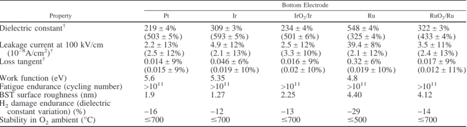
elec-trodes on the properties of BST film capacitors are summarized in Table I.
IV. Conclusions
The crystallinity and electrical properties of BST films de-posited on Pt, Ir, IrO2/Ir, Ru, and RuO2/Ru bottom electrodes
strongly depend on annealing conditions. We have shown that a BST thin film deposited on Ru at 500°C has a dielectric constant of 548 ± 4%, a loss tangent of 0.32 ± 6% at 100 kHz, a leakage current of (3.94 ± 8%) × 10−7A/cm2at an electric
field of 100 kV/cm with a delay time 30 s, and a charge storage density of 49 ± 4% fC/m2at an applied field of 150 kV/cm.
After the BST deposited on Ru capacitor is annealed in O2at
700°C for 20 min, the loss tangent decreases to 0.019 ± 10% and the leakage current decreases to (2.1 ± 12%) × 10−8A/cm2
at an electric field of 100 kV/cm with a delay time of 30 s. A BST thin film deposited on Ir at 500°C after 700°C annealing in O2for 20 min has a dielectric constant of 593 ± 5%, a loss
tangent of 0.019 ± 10% at 100 kHz, a leakage current of (2.1 ± 13%) × 10−8A/cm2at an electric field of 100 kV/cm
with a delay time 30 s, and a charge storage density of 53 ± 5% fC/m2at an applied field of 150 kV/cm. Based on the
dielec-tric constant, leakage current, and reliability, the optimum material for the bottom electrode with annealing is Ir. The Ru electrode is unstable, because interdiffusion of Ru and Ti occurs at the interface between BST and Ru after anneal-ing. The extrapolated 10 year lifetime of TDDB studies
indi-cates that BST films on Pt, Ir IrO2/Ir, and Ir (600°C) have a
longer lifetime at 1 V operating voltage than those on Ru and RuO2/Ru.
Acknowledgment: Dr. P. Lin is thanked for helpful discussions.
References
1Y. Ohno, T. Horikawa, H. Shinkawata, K. Kashihara, T. Kuroiwa, T.
Oku-daira, Y. Hashizume, K. Fukumoto, T. Eimori, T. Shibano, K. Arimoto, H. Itoh, T. Nishimura, and H. Miyoshi, ‘‘A Memory Cell Capacitor with BaxSr1−xTiO3
(BST) Film for Advanced DRAMs,’’ Symp. VLSI Tech. Dig. Tech. Pap., 149–50 (1994).
2T. Eimori, Y. Ohno, J. Matsufusa, S. Kishimura, A. Yoshida, H. Sumitani,
T. Maruyama, Y. Hayashide, K. Moriizumi, T. Katayama, M. Asakura, T. Horikawa, T. Shibano, H. Itoh, K. Namba, T. Nishimura, S. Satoh, and H. Miyoshi, ‘‘A Newly Designed Planar Stacked Capacitor Cell with High Dielec-tric Constant Film for 256 Mbit DRAM,’’ IEDM Tech. Dig., 631–34 (1993).
3E. Fujii, Y. Uemoto, S. Hayashi, T. Nasu, Y. Shimada, A. Matsuda, M. Kibe,
M. Azuma, T. Otsuki, G. Kano, M. Scott, L. D. Mcmillan, and C. A. Paz de Araujo, ‘‘ULSI DRAM Technology with Ba0.7Sr0.3TiO3Film of 1.3 nm
Equiva-lent SiO2Thickness and 10
−9(A/cm2) Leakage Current,’’ IEDM Tech. Dig.,
267–70 (1992).
4K. Koyama, T. Sakuma, S. Yamamichi, H. Watanabe, H. Aoki, S. Ohya, Y.
Miyasaka, and T. Kikkawa, ‘‘A Stacked Capacitor with BaxSr1−xTiO3for 256M
DRAM,’’ IEDM Tech. Dig., 823–26 (1991).
5T. Y. Tseng, ‘‘Fabrication and Characterization of Electroceramic Thin
Films for Semiconductor Memory Applications,’’ Proc. Int. Electron Devices
Mater. Symp., C2–5, 89–96 (1996).
6T. Horikawa, N. Mikami, T. Makita, J. Tanimura, M. Kataoka, K. Sato, and
M. Nunoshita, ‘‘Dielectric Properties of (Ba,Sr)TiO3Thin Film Deposited by rf
Sputtering,’’ Jpn. J. Appl. Phys., 32, 4216–30 (1993).
7T. Kuoiwa, Y. Tsunenine, T. Horikawa, T. Makita, J. Tanimura, N. Mikami,
and K. Sato, ‘‘Dielectric Properties of (BaxSr1−x)TiO3Thin Films Prepared by
rf Sputtering for Dynamic Random Access Memory Application,’’ Jpn. J. Appl.
Phys., 33, 5187–91 (1994).
8R. Khamankar, B. Jiang, R. Tsu, W. Y. Hsu, J. Nulman, S. Summerfelt, M.
Anthony, and J. Lee, ‘‘A Novel Low-Temperature Process for High Dielectric Constant BST Thin Films for ULSI DRAM Applications,’’ Symp. VLSI Tech.
Dig. Tech. Pap., 127–28 (1995).
9S. G. Yoon and A. Safari, ‘‘(Ba
0.5,Sr0.5)TiO3Thin Film Preparation by rf
Magnetron Sputtering and Its Electric Properties,’’ Thin Solid Films, 254, 211– 15 (1995).
10S. O. Park, C. S. Hwang, H. J. Cho, C. S. Kang, H. K. Kang, S. I. Lee, and
M. Y. Lee, ‘‘Fabrication and Electrical Characterization of Pt/(Ba,Sr)TiO3/Pt
Capacitors for Ultralarge-Scale Integrated DRAM Applications,’’ Jpn. J. Appl.
Phys., 35, 1548–52 (1996).
11S. C. Sun, M. S. Tasi, P. Lin, J. A. Lay, D. C. H. Yu, and M. S. Liang,
‘‘Effect of Oxygen to Argon Ratio on Properties of (Ba,Sr)TiO3Thin Films
Prepared by rf Sputtering,’’ ECS Meet. Abstr., 96–1, 184–85 (1996).
12H. Kobayashi and T. Kobayashi, ‘‘Heteroepitaxial Growth of Quaternary
BaxSr1−xTiO3Thin Films by ArF Excimer Laser Ablation,’’ Jpn. J. Appl. Phys.,
33, L533–L536 (1994).
13W. J. Lee, I. K. Park, G. E. Jang, and H. G. Kim, ‘‘Electrical Properties and
Crystal Structure of (Ba0.5,Sr0.5)TiO3Thin Films Prepared on Pt/SiO2/Si by rf
Magnetron Sputtering,’’ Jpn. J. Appl. Phys., 34, 196–99 (1995).
14K. Takemura, S. Yamamichi, P. Y. Lesaicherre, K. Tokashiki, H.
Miya-moto, H. Ono, Y. Miyasaka, and M. Yoshida, ‘‘RuO2/TiN-Based Storage
Elec-trodes for (Ba,Sr)TiO3Dynamic Random Access Memory Capacitors,’’ Jpn. J.
Appl. Phys., 34, 5224–29 (1995).
15T. Sakuma, S. Yamamichi, S. Matsubara, H. Yamaguchi, and Y. Miyasaka,
‘‘Barrier Layers for Realization of High Capacitance Density in SrTiO3Thin
Film Capacitor on Silicon,’’ Appl. Phys. Lett., 57, 2431–33 (1990).
16Y. Fukuda, K. Numata, K. Aoki, and A. Nishimura, ‘‘Origin of Dielectric
Relaxation Observed for Ba0.5Sr0.5TiO3Thin Film Capacitor,’’ Jpn. J. Appl.
Phys., 35, 5178–80 (1996).
Table I. Properties of BST Thin Films Deposited on Various Bottom Electrode Materials Property
Bottom Electrode
Pt Ir IrO2/Ir Ru RuO2/Ru
Dielectric constant† 219 ± 4% 309 ± 3% 234 ± 4% 548 ± 4% 322 ± 3% (503 ± 5%) (593 ± 5%) (501 ± 6%) (325 ± 4%) (433 ± 4%) Leakage current at 100 kV/cm 2.2 ± 13% 4.9 ± 12% 2.5 ± 12% 39.4 ± 8% 3.5 ± 11% (10−8 A/cm2 )† (2.5 ± 12%) (2.1 ± 13%) (3.3 ± 10%) (2.1 ± 12%) (2.4 ± 13%) Loss tangent† 0.014 ± 9% 0.046 ± 6% 0.016 ± 9% 0.32 ± 6% 0.017 ± 9% (0.015 ± 9%) (0.019 ± 10%) (0.02 ± 10%) (0.019 ± 10%) (0.012 ± 11%)
Work function (eV) 5.6 5.35 4.8
Fatigue endurance (cycling number) >1011
>1011
>1011
>1011
>1011
BST surface roughness (nm) 1.9 1.27 2.25 4.40 4.12
H2damage endurance (dielectric
constant variation) (%) −16 −12 −13 −29 −14
Stability in O2ambient (°C) ⱕ700 ⱕ700 ⱕ700 ⱕ500 ⱕ700
†Numbers in parentheses are after annealing for 20 min at 700°C in O 2.
17C. S. Hwang, S. O. Park, H. J. Cho, C. S. Kang, H. K. Kang, S. I. Lee, and
M. Y. Lee, ‘‘Deposition of Extremely Thin (Ba,Sr)TiO3Thin Films for Ultra
Large Scale Integrated Dynamic Random Access Memory Application,’’ Appl.
Phys. Lett., 67, 2819–21 (1995).
18N. Ichinose and T. Ogiwara, ‘‘Preparation and Rapid Thermal Annealing
Effect of (Ba,Sr)TiO3Thin Films,’’ Jpn. J. Appl. Phys., 34, 5198–201 (1995). 19H. Matsuhashi and S. Nishikawa, ‘‘Optimum Electrode Materials for Ta
2O5
Capacitors for High and Low Temperature Processes,’’ Jpn. J. Appl. Phys., 33, L293–L297 (1994).
20M. S. Tsai, S. C. Sun, and T. Y. Tseng, ‘‘Effect of Bottom Electrode
Ma-terials on the Electrical and Reliability Characteristics of (Ba,Sr)TiO3
Capaci-tors,’’ IEEE Trans. Electron Devices, in review.
21S. C. Sun and M. S. Tsai, ‘‘Effect of Bottom Electrode Materials on the
Electrical and Reliability Characteristics of (Ba,Sr)TiO3Capacitors,’’ IEDM
Tech. Dig., Session 10.3 (1997).
22M. Yoshida, H. Yamaguchi, T. Sakuma, and Y. Miyasaka, ‘‘Chemical
Vapor Deposition of (Ba,Sr)TiO3,’’ J. Electrochem. Soc., 142, 244–48 (1995). 23T. S. Kim, M. H. Oh, and C. H. Kim, ‘‘Influences of Indium Tin Oxide
Layer on the Properties of rf Magnetron-Sputtered (Ba,Sr)TiO3Thin Films on
Indium Tin Oxide-Coated Glass Substrate,’’ Jpn. J. Appl. Phys., 32, 2837–41 (1993).
24P. Li, J. F. Mcdonald, and T. M. Lu, ‘‘Densification Induced Dielectric
Properties Change in Amorphous BaTiO3 Thin Films,’’ J. Appl. Phys., 71,
5596–600 (1992).
25M. S. Tsai, S. C. Sun, and T. Y. Tseng, ‘‘Effect of Oxygen to Argon Ratio
on Properties of (Ba,Sr)TiO3Thin Films Prepared by Radio-Frequency
Mag-netron Sputtering,’’ J. Appl. Phys., 82 [7] 3482–87 (1997).
26R. Khamankar, J. Kim, B. Jiang, C. Sudhama, P. Maniar, R. Moazzami, R.
Jones, and J. Lee, ‘‘Impact of Post Processing Damages on the Performance of High Dielectric Constant PLZT Thin Film Capacitors for ULSI DRAM Appli-cation,’’ VLSI Tech. Dig., 119–21 (1995).
27H. Miki, K. K. Abdelghafar, K. Torii, and Y. Fujisaki, ‘‘Hydrogen-Related
Degradation and Recovery Phenomena in Pb(Zr,Ti)O3Capacitors with a
Plati-num Electrode,’’ Jpn. J. Appl. Phys., 36, 1132–35 (1997).
28S. Takatani, K. K. Abdelghafar, and H. Miki, ‘‘Effect of H
2Annealing on
a Pt/PbZrxTi1−xO3 Interface Studied by X-ray Photoelectron Spectroscopy,’’
Jpn. J. Appl. Phys., 36, L435–L438 (1997).
29Y. Shimamoto, K. K. Abdelghafar, H. Miki, and Y. Fujisaki, ‘‘H 2Damage
of Ferroelectric Pb(Zr,Ti)O3Thin Film Capacitors—The Role of Catalytic and
Adsorptive Activity of the Top Electrode,’’ Appl. Phys. Lett., 70, 3096–97 (1997).
30L. H. Parker and A. F. Tasch, ‘‘Ferroelectric Material for 64 Mb DRAMs,’’
IEEE Circuits Devices Mag., 17–26 (1990).
31P. Hiergeist, A. Spitzer, and S. Rohl, ‘‘Lifetime of Thin Oxide and Oxide–
Nitride–Oxide Dielectrics within Trench Capacitors for DRAM’s,’’ IEEE
Trans. Electron Devices, 36, 913–19 (1989).
32M. S. Tsai and T. Y. Tseng, ‘‘Conduction Mechanisms and
Temperature-Dependent Current–Voltage in (Ba,Sr)TiO3Thin Films,’’ J. Electrochem. Soc.,
145 [8] 2853–60 (1998).
33M. S. Tsai and T. Y. Tseng, ‘‘Effect of Bottom Electrodes on Resistance
Degradation and Breakdown of (Ba,Sr)TiO3Thin Films,’’ IEEE Trans.
Com-pon. Packag. Manuf. Technol.—A, submitted.
34G. W. Dietz, W. Antpohler, M. Klee, and R. Waser, ‘‘Electrode Influence
on the Charge Transport through SrTiO3Thin Films,’’ J. Appl. Phys., 78,
6113–21 (1995).
35G. W. Dietz, M. Schumacher, R. Waser, S. K. Streiffer, C. Basceri, and
A. I. Kingon, ‘‘Leakage Current in Ba0.7Sr0.3TiO3Thin Films for Ultrahigh
Density Dynamic Random Memories,’’ J. Appl. Phys., 82, 2359–64 (1997).
36R. Waser, T. Baiatu, and K. H. Hardtl, ‘‘DC Electrical Degradation of
Perovskite Type Titanates: I, Ceramics,’’ J. Am. Ceram. Soc., 73, 1645–53 (1990).
37R. M. Waser, ‘‘Electrochemical Boundary Conditions for Resistance
Deg-radation of Doped Alkaline-Earth Titanates,’’ J. Am. Ceram. Soc., 72, 2234–40