IEEE ELECTRON DEVICE LElTERS. VOL. 16, NO. 9, SEPTEMBER 1995 385
The Electrical Characteristics of Polysilicon
Oxide Grown in Pure N2O
Chao
Sung
Lai,Tan Fu Lei,
and ChungLen
Lee,
Senior Member,ZEEE
Abstract-NzO was used to grow silicon polyoxide. It was found that the Nz0-grown polyoxide had a lower leakage current but a higher breakdown field when the top-electrode was positively
biased. This is opposite to that of conventional 02-grown poly- oxide. Moreover, it had less electron trapping when stressed and a larger charge-to-breakdown.
I. INTRODUCTION
N order to obtain good data retention characteristics for
I
nonvolatile memory, the inter-polysilicon oxides (polyox- ides) with low conductivity and high breakdown fields have long been sought [ 11-[4]. For example, textured polysilicon oxides have been widely used in nonvolatile memory [3], [4]. Recently, N2O used as an oxidant or a post-oxidation annealing ambient for gate dielectrics has received much attention due to its endurance to Fowler-Nordheim (F-N) stress, which is thought to derive from its incorporation of nitrogen at the oxide-silicon interface [ 5 ] ,[SI.
However, growth of polyoxides in pure N2O has not previously been reported.This letter reports on N2O used as an oxidant to grow poly- oxide. It was found that the grown polyoxide has very desirable qualities such as a polarity asymmetry of J-E characteristics, which has a lower leakage current but a higher breakdown field when the top electrode is positively biased; and a higher charge-to-breakdown ( Q b d ) .
11. EXPERIMENTS
The polyoxides were prepared by oxidizing polysilicon films. P-type wafers were thermally oxidized to a thickness of 100 nm. Then, a 300 nm polysilicon film (pdy 1) was deposited at 625°C and doped with POC13. A one-hour drive- in process was performed in ambient N2 at 900°C to activate the dopant; the sheet resistance of the resulting polysilicon film was 22
Q/O.
Polyoxides grown in pure N2O at 900°C were made to a thickness of about 14 nm. For comparison, polyoxides grown in pure O2 at 90O0C were also prepared. Then, a second layer of polysilicon (poly 2) of 300 nm thick was deposited and also doped with POC13 to a sheet resistance of 22a / ! .
After defining poly 2, all samples received a 100 nm thick oxide via wet oxidation as a passivation layer. Contact Manuscript received March 15, 1995; revised May 24, 1995. This work was supported by the National Science Council, R.O.C., under Contract NSC-84- 2215-E-009-003.The authors are with the National Chiao Tung University, Department of Electronic Engineering and Institute of Electronics, Hsinchu 300, Taiwan, R.O.C.
IEEE Log Number 9413797.
10-1 1 0 3 1 0 5 1
o - ~
0 24
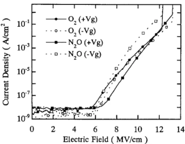
6 8 1 0 1 2 1 4 Electric Field ( MV/cm )The J-E characteristics of N2O-grown and 02-grown polyoxide Fig. 1.
devices. Both polyoxides were 14 nm thick.
holes were opened, and A1 was deposited and patterned to form capacitors. Finally, all devices were sintered at 350OC for 40 minutes in N2 gas.
111. RESULTS AND DISCUSSION
The oxidation rate of this heavily-doped polysilicon was more than three times faster than the oxidation rate of the lightly-doped Si substrate in pure N20 and the self-limiting phenomenon, which exists for N20 oxidation on Si
[SI,
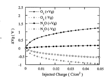
was not observed. The typical J-E characteristics of NzO-grown polyoxide is shown in Fig. 1 along with those of 02-grown control polyoxide. It can be seen that the NzO polyoxide conducted a lower leakage current and had a higher breakdown field when the poly 2 was positively biased, whose electrons were injected from the lower polyoxide-poly 1 interface. This polarity asymmetry is opposite to that of the 02-grown polyoxide and can be attributed to the interface roughness [4], [9]. The NzO-grown palyoxide had a higher current density at dielectric breakdown.','Fig. 2 shows the trapping behavior of N2O-grown poly- oxide. The capacitor area was 5 x lop4 cm2 and the stress condition was 1 mA/cm2 constant current injection for both positive and negative bias. It can be seen that the N20-grown polyoxide had smaller voltage shifts, with both the positive and negative bias stress. This means that the N20-grown polyoxide trapped fewer electrons. The O2-grown polyoxide Vg shifts were almost the same for both polarity stressing, but for the N2O-grown polyoxide, positive stress Vg shift 0741-3106/95$04.00 0 1995 IEEE
386
.
IEEE ELECTRON DEVICE L E T E R S , VOL. 16, NO. 9, SEPTEMBER 19950 0.01 0.02 0.03 0.04 0.05
Injected Charge ( C/cm2 )
Fig. 2. The voltage shifts of the NZO-grown polyoxide and the 02-grown polyoxide devices under positive and negative constant current stress of
1 mA/cm2. The gate area was 5 x cm2.
was significantly lower than its negative stress Vg shift. This difference was due to nitrogen pile-up at the N2O-grown polyoxide/poly 1 interface.
Fig. 3 shows the Weibull charge-to-breakdown plot for
40 N2O-grown and 02-grown polyoxide capacitors under 1
mA/cm2 stress. The N2O-grown polyoxide had larger Q b d and
narrower Q b d distribution than did the 02-grown polyoxide.
This improved Q b d of the N2O-grown polyoxide was due to the reduced electron trapping which is shown in Fig. 2. Moreover, the Q b d improvement of N20-grown polyoxide
is the most apparent for negative bias stress. The 02-grown polyoxides had more defect-related breakdowns in the lower
Q b d region, but the N20-grown polyoxides had more intrinsic breakdowns. From Figs. 2 and 3, Q b d is greater when top-
electrode of polyoxide is biased such that injection occurs at the “leakier” interface. For N2O-grown polyoxide, it is negative bias; for 02-grown polyoxide it is positive bias. This is in agreement with the hole-trapping breakdown model, which predicts that Q b d increases as the anode field decreases
191, [lo].
IV. CONCLUSION
In conclusion, the above results show that the polyoxide grown in N2O has improved integrity over conventional 02- grown polyoxides. It has desirable J-E polarity asymmetry of
J-E characteristic, i.e., lower leakage current and higher E b d ,
-3
’
‘ ‘ ’ t m t l a ’ -nn1
o - ~
10’loo
Charge to breakdown ( C/cm2 )
Fig. 3. The Weibull charge-to-breakdown plots for NzO-grown and 02-grown polyoxide devices under positive and negative stress. The stress condition was 1 mA/cm2 and the gate area was 5 x cm2.
when the top electrode is positively biased, reduced electron trapping and a larger Q b d than the conventional 02-grown
polyoxides.
REFERENCES
[I] C. Cobianu, 0. Popa, and D. Dascalu, “On the electrical conduction in the dielectric layers,” IEEE Electron Device Lett., vol. 14, p. 213, 1993. [2] H. N. Chern, C. L. Lee, and T. F. Lei, “Improvement of polysilicon oxide characteristics by fluorine incorporation,” IEEE Electron Device Lert., vol. 15, p. 181, 1994.
[3] T. Ono, T. Mori, T. Ajioka, and T. Takayashiki, “Studies of thin poly-Si oxides for E and E2PROM,” IEDM Tech Dig., pp. 3%-383, 1985. [4] S. L. Wu, T. Y. Lin, C. L. Lee, and T. F. Lei, “Electrical characteristics
of textured polysilicon oxide prepared by a low-temperature wafer loading and NZ preannealing process,” IEEE Electron Device Len., vol.
14, p. 113, 1994.
[5] J. Ahn, W. Ting, and D. L. Kwong, “Furnace nitridation of thermal Si02 in pure N 2 0 ambient for ULSI MOS application,” IEEE Electron Device Lett., vol. 13, p. 117, 1992.
[6] Z. Liu, H. J. Wann, P. K. KO, C. Hu, and Y. C. Chang, “Effects of NzO anneal and reoxidation on thermal oxide characteristics,” IEEE Electron Device Lett., vol. 13, p. 402, 1992.
[7] -, “The effects of furnace NzO annealing on MOSFET’s,” IEDM
Tech. Dig., p. 625, 1992.
[8] H. Hwang, W. Ting, D. L. Kwong, and J. Lee, “Electrical and reliability characteristics of the ultrathin oxynitride prepared by rapid thermal processing in NzO,” IEDM Tech Dig., p. 421, 1990.
[9] J. C. Lee and C. Hu, “Polarity asymmetry of oxides grown on polycrys- talline silicon,” IEEE Truns. Electron Devices, vol. 35, no. 7, p. 1063, July 1988.
[lo] I. C. Chen, S. Holland, and C. Hu, “Electrical breakdown in thin gate and tunneling oxides,” IEEE Truns. Electron Devices, vol. ED-32, no. 2, p. 413, Feb. 1985.