AlGaN/GaN high electron mobility transistors with a low sub-threshold swing on
free-standing GaN wafer
Xinke Liu, Hong Gu, Kuilong Li, Lunchun Guo, Deliang Zhu, Youming Lu, Jianfeng Wang, Hao-Chung Kuo,
Zhihong Liu, Wenjun Liu, Lin Chen, Jianping Fang, Kah-Wee Ang, Ke Xu, and Jin-Ping Ao
Citation: AIP Advances 7, 095305 (2017); doi: 10.1063/1.4999810 View online: http://dx.doi.org/10.1063/1.4999810
View Table of Contents: http://aip.scitation.org/toc/adv/7/9
Published by the American Institute of Physics
Articles you may be interested in
Three-dimensional steady and transient fully coupled electro-thermal simulation of AlGaN/GaN high electron mobility transistors: Effects of lateral heat dissipation and thermal crosstalk between gate fingers
AIP Advances 7, 095304 (2017); 10.1063/1.5002544
FEM thermal and stress analysis of bonded GaN-on-diamond substrate
AIP Advances 7, 095105 (2017); 10.1063/1.4995005
A numerical model for investigation of emission of particle debris from laser-irradiated metal targets
AIP Advances 7, 095005 (2017); 10.1063/1.4991398
Effect of total emitted electron velocity distribution function on the plasma sheath near a floating wall
AIP Advances 7, 085220 (2017); 10.1063/1.5000507
Effect of Si doping on the thermal conductivity of bulk GaN at elevated temperatures – theory and experiment
AIP Advances 7, 095302 (2017); 10.1063/1.4989626
Evolution of threading dislocations in GaN epitaxial laterally overgrown on GaN templates using self-organized graphene as a nano-mask
AlGaN/GaN high electron mobility transistors with a low
sub-threshold swing on free-standing GaN wafer
Xinke Liu,1,aHong Gu,1Kuilong Li,1Lunchun Guo,1Deliang Zhu,1
Youming Lu,1Jianfeng Wang,2Hao-Chung Kuo,3Zhihong Liu,4
Wenjun Liu,5Lin Chen,5Jianping Fang,6Kah-Wee Ang,4Ke Xu,2
and Jin-Ping Ao1,a
1College of Materials Science and Engineering, Shenzhen Key Laboratory of Special Functional Materials, Chinese Engineering and Research Institute of Microelectronics, Shenzhen University, Shenzhen 518060, People’s Republic of China
2Suzhou Institute of Nano-Tech and Nano-Bionics (SINANO), CAS, Suzhou 215123, People’s Republic of China
3Department of Photonics and Institute of Electro-Optical Engineering, National Chiao Tung University, Hsinchu 300, Taiwan
4Department of Electrical and Computer Engineering, National University of Singapore, 117583, Singapore
5Department of Microelectronics, Fudan University, Shanghai 200433, People’s Republic of China
6School of Microelectronics, Xidian University, Xi’an 710071, People’s Republic of China
(Received 3 May 2017; accepted 30 August 2017; published online 8 September 2017)
This paper reported AlGaN/GaN high electron mobility transistors (HEMTs) with low sub-threshold swing SS on free-standing GaN wafer. High quality AlGaN/GaN epi-layer has been grown by metal-organic chemical vapor deposition (MOCVD) on free-standing GaN, small full-width hall maximum (FWHM) of 42.9 arcsec for (0002) GaN XRD peaks and ultralow dislocation density (∼104-105 cm-2) were obtained.
Due to these extremely high quality material properties, the fabricated AlGaN/GaN HEMTs achieve a low SS (∼60 mV/decade), low hysteresis of 54 mV, and high peak electron mobility µeff of ∼1456 cm2V-1s-1. Systematic study of materials properties
and device characteristics exhibits that GaN-on-GaN AlGaN/GaN HEMTs are promis-ing candidate for next generation high power device applications. © 2017 Author(s). All article content, except where otherwise noted, is licensed under a Creative Commons Attribution (CC BY) license (http://creativecommons.org/licenses/by/4.0/). [http://dx.doi.org/10.1063/1.4999810]
I. INTRODUCTION
Gallium nitride (GaN)-based power device, e.g. Schottky barrier diodes (SBDs) and high electron mobility transistors (HEMTs), have attracted considerable research interest and well recognized as the next generation high power and high temperature devices, owing to their ultralow conduction loss and fast switching under high voltage and high frequency operations.1–3However, these devices have been mostly fabricated on foreign substrates, such as silicon, sapphire, and SiC, and the major challenge is a high density of threading dislocations (∼108-1010cm-2) originating from the strained heteroepitaxial growth on the foreign substrate, which becomes problematic for devices under high power operation.4–8 For GaN heteroepitaxial growth, various material growth technologies have
been proposed to improve the GaN epi-quality on the top surface of wafer or in the channel region of the devices. Thick buffer layer made of low-temperature GaN,9 AlN,10AlGaN,11or multi-pairs of
alternate AlN/GaN layer12–15has been used to eliminate the propagation of the threading dislocation
toward the wafer surface, the drawback is that there is a very defective transition layer between GaN and foreign substrate, which could result in reliability issues (e.g. substrate leakage, poor thermal
095305-2 Liu et al. AIP Advances 7, 095305 (2017)
dissipation), although efforts can be made to improve the buffer quality, such as Fe or C doping.16,17 Recently, the availability of sufficiently large GaN substrates has enabled the homoepitaxial growth of GaN-based devices.18–20Free-standing GaN, grown by hydride vapor phase epitaxy (HVPE), can
offer a threading dislocation density less than 106cm-2, which shows promise to further enhance the
GaN-based device performance. As reported in the literature, low sub-threshold swing SS has been obtained for AlGaN/GaN-on-silicon HEMTs (SS ∼64 mV/decade) by reducing gate leakage using O2 plasma treatment,21 and AlInN/AlN/GaN-on-SiC HEMTs (SS less than 40 mV/decade) due to
the effect of negative capacitance.22
In this work, AlGaN/GaN epi-layer was grown by metal-organic chemical vapor deposition on 2 inch semi-insulating Fe-doped free-standing GaN substrate with (0001) orientation. It is revealed that the AlGaN/GaN epi-layer on free-standing wafer shows extremely low dislocation density, which ensure that the fabricated AlGaN/GaN HEMTs achieve a low sub-threshold swing. Transmis-sion electron microscopy (TEM), atomic force microscopy (AFM), high-resolution X-ray diffraction (HR-XRD), and cathodoluminescence (CL) were employed to study the quality of the AlGaN/GaN epi-layer. Electrical characterization was also performed for the fabricated AlGaN/GaN HEMTs on the free-standing GaN wafer.
II. EXPERIMENT DETAILS
Two inch semi-insulating Fe-doped free-standing GaN substrate (350 µm thick) with (0001) orientation was grown by hydride vapor phase epitaxy (HVPE). HCl/metal Ga, ammonia, and N2/H2
mixture were used as gallium source, nitrogen source, and carrier gas, respectively. The growth rate was typically about 150µm/hour. After HVPE growth, the Ga surface was further polished by chemical mechanical polishing (CMP). Heterostructure Al0.25Ga0.75N(27 nm)/GaN(1 µm) epi-layer
was grown on the Ga surface of free-standing GaN by metal-organic chemical vapor deposition (MOCVD). After active region formation using Cl2-based reactive ion etching, pre-gate
clean-ing consisted of a 2-minute acetone and a 3-minute isopropanol degreasclean-ing step, followed by a 10-minute dilute HCl (H2O:HCl=1:1) native oxide removal step, and an ex situ surface passivation
step by immersion in a (NH4)2S solution for 30 minutes.23,24 Ti(50 nm)/Al(200 nm)/Ti(40 nm)/
Au(40 nm) stack was deposited as source/drain electrode using E-beam evaporator, and formed ohmic contact after 850oC annealing for 60s in N2ambient. Ni(70 nm)/Au(30 nm) was deposited by
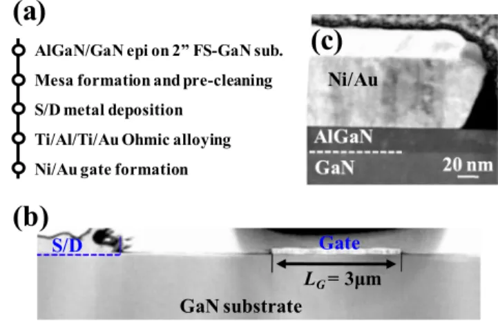
E-beam evaporator and gate electrode was formed using a lift-off process. No passivation layer was deposited on the fabricated AlGaN/GaN HEMTs in this work. Fig.1(a)shows the fabrication process used in this work. The gate length LGand gate-to-drain/source spacing of the fabricated device is 3
and 3.5 µm, respectively, which is shown in Fig.1(b). The GaN substrate shows a clean surface with-out dislocation line or 2 dimensional defect, which can be frequently observed for GaN-on-silicon
FIG. 1. (a) Process flow of fabricating AlGaN/GaN HEMTs. Cross-sectional TEM image of (b) device and (c)Ni-Au/ AlGaN/GaN gate stack.
or GaN-on-sapphire wafers. Fig. 1(c)shows the cross-sectional transmission electron microscopy (TEM) image of Ni-Au/AlGaN/GaN gate stack of the fabricated device.
III. RESULTS AND DISCUSSION
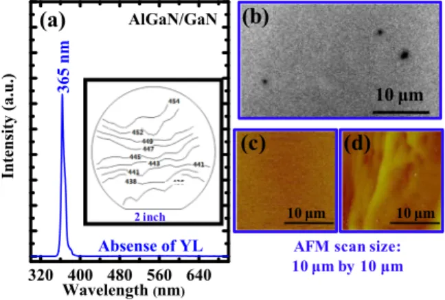
Fig.2(a)shows the room-temperature photoluminescence (PL) spectrum of AlGaN/GaN epi-layer on free-standing GaN, and a strong peak due to the near-band-edge ultraviolet (UV) transition located at a wavelength of 365 nm (3.4 eV) is observed. As reported in the literature,25a broad yellow luminescence (YL) centered at 2.2 eV can be observed, and this is due to the recombination of carriers between a shallow donor related to oxygen substitutional to the nitrogen site and a deep acceptor due to gallium vacancies, or due to the defects related to carbon related defects.22–27The absence of YL
in Fig.1(a)indicates a low defect density in the AlGaN/GaN epi-layer, which is the main reason that the fabricated AlGaN/GaN HEMTs can achieve a low sub-threshold swing. The inset of Fig.2(a) shows the sheet resistance Rshmapping of the as-grown AlGaN/GaN epi-layer on 2 inch free-standing
GaN, and an average Rshof 445 ohm/square and an average Hall mobility of ∼1500 cm2V-1s-1are
obtained. The dislocation density of AlGaN/GaN epi-layer is measured by cathodoluminescence and is in the range of ∼104-105 cm-2, as shown in Fig.2(b). The level of dislocation density (∼104-105 cm-2) is few orders of magnitude lower than that for GaN-on-silicon and GaN-on-sapphire wafers (∼108-1010 cm-2). The root-mean-square (rms) before and after AlGaN/GaN epi-layer growth is measured to be 0.3 and 1.1 nm, respectively, by AFM shown in Fig. 2(c) and (d). The surface morphology or roughness for the free-standing GaN wafer before AlGaN/GaN epi-layer growth is determined by the CMP process. After AlGaN/GaN epi-layer growth, the surface roughness increased and surface morphology can be clearly seen from Fig.2(d).
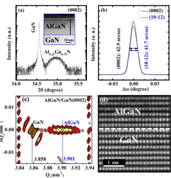
As shown in Fig. 3(a), the high resolution X-ray diffraction (HR-XRD) was performed on AlGaN/GaN epi-layer to confirm the composition (Al fraction: 0.25) and the crystal quality of the Al0.25Ga0.75N epitaxial layer. The full width half maximum (FWHM) of AlGaN (0002) peak
is ∼ 0.32◦. The thickness of AlGaN layer is measured to be ∼27 nm from a cross-sectional TEM
image shown as an inset of Fig.3(a). XRD (0002) and (10-12) rocking curves of GaN peak is shown in Fig.3(b), in which the FWHM of (0002) and (10-12) planes is 42.9 and 41.7 arcsec, respectively, which is significantly lower than that of GaN-on-silicon and GaN-on-sapphire wafers (300-800 arcsec). Fig.3(c)shows the (0002) XRD reciprocal lattice space map of the c-plane AlGaN/GaN heterostruc-ture. The diffraction spot of AlGaN layer is located above the GaN layer, indicating the AlGaN layer is coherently grown on the GaN layer along the c-axis, and AlGaN layer is subjected to a tensile strain (∼1.8%).28With the (0002) reciprocal space map shown in Fig.3(c), the lattice constant (c) for GaN and AlGaN is measured to be 0.5184 and 0.5127 nm, respectively, using the equation c=2/Qz,
FIG. 2. (a) Room-temperature photoluminescence (PL) spectrum of AlGaN/GaN epi-layer on free-standing GaN, and a strong peak due to the near-band-edge ultraviolet (UV) transition located at a wavelength of 365 nm (3.4 eV) is observed, and inset shows the sheet resistance map of AlGaN/GaN epi. (b) cathodoluminescence image of AlGaN/GaN surface. AFM images of (c) before and (d) after AlGaN/GaN epi-layer growth.
095305-4 Liu et al. AIP Advances 7, 095305 (2017)
FIG. 3. (a) HR-XRD of AlGaN/GaN epi layer on free-standing GaN wafer (inset: cross-sectional TEM image of AlGaN/GaN layer). (b) Rocking curves of GaN (0002) and (10-12) peaks. (c) (0002) XRD reciprocal lattice space map of the c-plane AlGaN/GaN heterostructure. (d) HR-TEM of AlGaN/GaN heterostructure on FS-GaN substrate.
FIG. 4. (a) Drain current versus gate voltage (ID-VG) characteristics at drain voltage VD= 0.5, 1.0, 1.5, and 2 V of AlGaN/GaN HEMTs (gate length LG=3 µm and gate width W =25µm). The inset shows the actual fabricated HEMTs in this work. (b) Drain current versus drain voltage (ID-VD) characteristics of AlGaN/GaN HEMTs, where the maximum gate voltage VG,maxis 1V, and step is -1V. (c) Gate capacitance as a function of gate voltage under 1MHz. (d) Effective electron mobility µ as a function of carrier density Ns.
where Qz is the scattering vector in the [0001] direction. Fig.3(d)shows the high-resolution TEM
image of perfect lattice structure of AlGaN/GaN heterostructure in this work, which further confirm the quality of AlGaN/GaN epi-layer.
Fig.4(a)shows the drain current versus gate voltage (ID-VG) characteristics at drain voltage
VD= 0.5, 1.0, 1.5, and 2 V of AlGaN/GaN HEMTs (gate length LG=3 µm and gate width W = 25
µm). The inset shows the actual fabricated HEMTs in this work. A threshold voltage Vth of -3.1 V
was extracted using the linear-extrapolation method, which extrapolates the (ID-VG) characteristic
measured at VD= 0.5 V, from the point of maximum slope to the intercept with the gate voltage axis.
Fig.4(b)shows the drain current versus drain voltage (ID-VD) characteristics of AlGaN/GaN HEMTs,
where the maximum gate voltage VG,maxis 1V, and step is -1V. At a gate overdrive (VG Vth) of ∼4 V
and a drain voltage VD of 10 V, the saturation output drain current is ∼610 mA/mm, and the static
on-state resistance Ronextracted from the device active area is 0.5 mΩ.cm2. The output drain current
is comparable or high than that of GaN-on-silicon device, and this is could be due to high electron mobility resulted from less defect density. As shown in Fig.4(a), an average sub-threshold swing SS (∼67 mV/decade) is obtained over the three orders of drain current, in which a minimum average SS (∼60 mV/decade) is obtained over one order of drain current. It is noted that the SS value shown in Fig.4(a), such as 79 mV/dec., 60 mV/dec., and 62 mV/dec. is the average one for the drain current in the range of 1×10⁻⁷∼1×10⁻⁸A/µm, 1×10⁻⁸∼1×10⁻⁹A/µm, and 1×10⁻⁹∼1×10⁻¹⁰A/µm, respectively.
The effective interface state density Ditcan be estimated by the equation of sub-threshold swing SS:29
SS=kTq ln(10) × (1 +Cd+Cit
Cox ), where k is the Boltzmann constant, T is the temperature in Kelvin, q is the electronic charge, Cd is the depletion capacitance of GaN, Cit is the AlGaN/GaN interface state
capacitance, and Coxis the unit gate capacitance. As shown in Fig.4(c), the gate capacitance is plotted
as a function of gate voltage under a frequency of 1 MHz, and Cd/Coxratio is ∼0.2. With negligible
interface state Cit, the calculated SS by the equation SS=kTq ln(10) × (1 +CCoxd) is ∼71 mV/decade,
which is consistent with the experimental average SS value of 67 mV/decade. Fig.4(d)shows the effective electron mobility µ as a function of carrier density Ns. The carrier density Nswas obtained
FIG. 5. (a) Forward and reverse ID-VGplot at VD=1V. (b) Ion/Ioffand (c) SS as a function of IGof the fabricated AlGaN/GaN HEMTs. (d) Benchmarking of SS for GaN-on-GaN HEMTs (this work) and passivated GaNon-Si (or Al2O3) HEMTs.
095305-6 Liu et al. AIP Advances 7, 095305 (2017)
by integrating the area under the C-V curve shown in Fig.4(c). The effective electron mobility µ is extracted using µ=WL × Id
VdNs,
30where I
dis the drain current at a small Vdof 0.5 V. A peak effective
electron mobility µ of 1456 cm2/V.s is obtained at a carrier density of 1.2×1012cm-2.
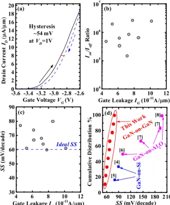
Fig. 5(a)shows the forward and reverse ID-VG plot at VD=1V, and very small hysteresis of
54 mV is obtained. Hysteresis is related to traps in the device, and slow traps can result in large hysteresis of ID-VG curve.31The small hysteresis here further indicates the high quality interface
in the gate region. Also, Ion/Ioff ratio and SS are plotted as a function of gate leakage current IGin
Fig.5(b)and(c). The average Ion/Ioff ratio, average SS, and average gate leakage IGis ∼1.2×10⁶,
∼68 mV/decade, and ∼7.0×10⁻¹¹A/µm respectively. Ionand Ioff is defined as the drain current at VD
of 1V under gate voltage of Vth+3V and Vth-2V, respectively. IGis defined as the gate leakage under
VDof 1V and Vth-2V. To further illustrate the advantage of free-standing GaN over GaN-on-silicon
and GaN-on-sapphire wafers, a cumulative plot of SS values of this work and ones from reported work is shown in Fig.5(d), from which it can be seen that AlGaN/GaN HEMTs on free-standing GaN wafer achieve the lowest SS value, as compared with other reported results using GaN-on-silicon and GaN-on-sapphire wafers.
IV. CONCLUSION
AlGaN/GaN high electron mobility transistors (HEMTs) with a low sub-threshold swing SS (∼60mV/decade) were fabricated on the extremely high quality free-standing GaN substrate. High quality AlGaN/GaN epi-layer has been grown on free-standing GaN in this work, such as ultralow FWHM for (0002) and (10-12) GaN XRD peaks, and ultralow dislocation density (∼104-105cm-2). Due to these extremely high quality material properties, the fabricated unpassivated AlGaN/GaN HEMTs achieve a low SS (∼60 mV/decade), low hysteresis of 54 mV, and high peak electron mobility µeff of ∼1456 cm2V-1s-1. As compared to the reported GaN-based HEMTs on sapphire or silicon
wafers, the GaN-on-GaN AlGaN/GaN HEMTs in this work have achieved the smallest or lowest SS.
ACKNOWLEDGMENTS
This project is supported by national key research and development plan (2017YFB0404100).
1C.-W. Tsou, K.-P. Wei, Y.-W. Lian, and S. S. H. Hsu,IEEE Electron Device Lett.37, 70 (2016).
2R. Chu, A. Corrion, M. Chen, R. Li, D. Wong, D. Zehnder, B. Hughes, and K. Boutros,IEEE Electron Device Lett.32, 632
(2011).
3B. Lu and T. Palacios,IEEE Electron Device Lett.31, 951 (2010).
4X. Liu, C. Zhan, K. W. Chan, W. Liu, L. S. Tan, K. J. Chen, and Y.-C. Yeo,Appl. Phys. Express5, 066504 (2012). 5W. H. Tham, L. K. Bera, D. S. Ang, S. B. Dolmanan, T. N. Bhat, and S. Tripathy,IEEE Electron Device Lett.36, 1291
(2015).
6X. Liu, B. Liu, E. K. F. Low, H.-C. Chin, W. Liu, M. Yang, L. S. Tan, and Y.-C. Yeo,IEDM Tech. Dig., 261 (2010). 7Y. Kong, J. Zhou, C. Kong, Y. Zhang, X. Dong, H. Lu, T. Chen, and N. Yang,IEEE Electron Device Lett.35, 336 (2014). 8K. J. Chen, S. Yang, Z. Tang, S. Huang, Y. Lu, Q. Jiang, S. Liu, C. Liu, and B. Li,Phys. Stat. Sol. (a)212, 1059 (2015). 9Y. Watanabe and M. Sano,Jpn. J. Appl. Phys.42, 384 (2003).
10P. Saengkaew, A. Dadgar, J. Blaesing, T. Hempel, P. Veit, J. Christen, and A. Krost,J. Cryst. Growth311, 3742 (2009). 11S. L. Selvaraj, T. Suzue, and T. Egawa,IEEE Electron Device Lett.30, 587 (2009).
12H. Umeda, A. Suzuki, Y. Anda, M. Ishida, T. Ueda, T. Tanka, and D. Ueda, IEDM Tech. Dig., 480 (2010). 13S. Arulkumaran, T. Egawa, S. Matsui, and H. Ishikawa,Appl. Phys. Lett.86, 123503 (2005).
14D. Visalli, M. V. Hove, J. Derluyn, S. Degroote, M. Leys, K. Cheng, M. Germain, and G. Borghs,Jpn. J. Appl. Phys.48,
04C101 (2009).
15S. Arulkumaran, S. Vicknesh, N. G. Ing, S. L. Selvaraj, and T. Egawa,Appl. Phys. Express4, 084101 (2011).
16Z. Bougrioua, M. Azize, A. Jimenez, A.-F. Branna, P. Lorenzini, B. Beaumont, E. Munoz, and P. Gibart,Phys. Stat. Sol.
(c)2, 2424 (2005).
17Y. Cao, R. Chu, R. Li, M. Chen, R. Chang, and B. Hughes,Appl. Phys. Lett.108, 062103 (2016).
18M. K. Kelly, R. R. Vaudo, V. M. Phanse, L. Gorgens, O. Ambacher, and M. Stutzmann,Jpn. J. Appl. Phys.38, L217 (1999). 19J. Q. Liu, J. F. Wang, Y. X. Qiu, X. Guo, K. Huang, Y. M. Zhang, X. J. Hu, Y. Xu, K. Xu, X. H. Huang, and H. Yang,
Semicond. Sci. Technol.24, 125007 (2009).
20J. Q. Liu, J. F. Wang, Y. F. Liu, K. Huang, X. J. Hu, Y. M. Zhang, Y. Xu, K. Xu, and H. Yang,J. Cryst. Growth311, 3080
(2009).
21J. W. Chung, J. C. Roberts, E. L. Piner, and T. Palacios,IEEE Electron Device Lett.29, 1196 (2008).
22H. W. Then, S. Dasgupta, M. Radosavljevic, L. Chow, B. Chu-Kung, G. Dewey, S. Gardner, X. Gao, J. Kavalieros,
23T. Maruyama, K. Yorozu, T. Noguchi, Y. Seki, Y. Saito, T. Araki, and Y. Nanishi,Phys. Stat. Sol. (c)0, 2031 (2003). 24Y.-L. Chiou, C.-S. Lee, and C.-T. Lee,Appl. Phys. Lett.97, 032107 (2010).
25Y. Saitoh, K. Sumiyoshi, M. Okada, T. Horii, T. Miyazaki, H. Shiomi, M. Ueno, K. Katayama, M. Kiyama, and T. Nakamura,
Appl. Phys. Express3, 081001 (2010).
26C. H. Seager and A. F. Wright,J. Appl. Phys.92, 6553 (2002).
27R. Armitage, W. Hong, Q. Yang, H. Feick, J. Gebauer, E. R. Weber, S. Hautakangas, and K. Saarinen,Appl. Phys. Lett.82,
3457 (2003).
28M. Tsuda, H. Furukawa, A. Honshio, M. Iwaya, S. Kamiyama, H. Amano, and I. Akasaki,Phys. Stat. Sol. (b)243, 1524
(2006).
29B. Lu, E. Matioli, and T. Palacios,IEEE Electron Device Lett.33, 360 (2012).
30H.-C. Chin, X. Liu, X. Gong, and Y.-C. Yeo,IEEE Trans. Electron Devices57, 973 (2010). 31H. Hasegawa, T. Inagaki, S. Ootomo, and T. Hashizume,J. Vac. Sci. Technol. B21, 1844 (2003).