Correlation between Exciton Lifetime Distribution and Morphology of Bulk Heterojunction
Films after Solvent Annealing
Jen-Hsien Huang,§ Kuang-Chieh Li,#Fan-Ching Chien,§Yu-Sheng Hsiao,§Dhananjay Kekuda,§
Peilin Chen,§Hong-Cheu Lin,#Kuo-Chuan Ho,†,‡and Chih-Wei Chu*,§,⊥
Research Center for Applied Sciences, Academia Sinica, Taipei, Taiwan 115, People’s Republic of China, Department of Chemical Engineering, National Taiwan UniVersity, Taipei, Taiwan 10617, People’s Republic of China, and Department of of Materials Science and Engineering, National Chiao Tung UniVersity, Hsinchu, Taiwan 30010, People’s Republic of China
ReceiVed: December 22, 2009; ReVised Manuscript ReceiVed: April 14, 2010
We have synthesized a low-bandgap polymer, bithiazole-based polymer (PCPDTTBT) containing cyclopen-tadithiophene and thiophene units, and studied its opticophysical properties and morphologies in bulk heterojunction films after annealing. We used confocal optical microscopy in conjunction with a fluorescence module to record exciton lifetime images within photoactive layers of PCPDTTBT and [6,6]-phenyl-C61
-butyric acid methyl ester (PCBM). These images, which were consistent with those recorded using atomic force microscopy and transmission electron microscopy, revealed that phase separation of PCPDTTBT and PCBM occurred during slow solvent evaporation. This phase separation not only provided bicontinuous pathways for carrier transport to the respective electrodes but also enhanced the degree of polymer chain stacking, thereby improving the absorption and balancing the electron and hole mobilities. We tested the performance of solar cells incorporating PCPDTTBT and various fullerene derivatives. Under AM 1.5 G illumination (100 mW cm-2), a PCPDTTBT/bisPCBM-based solar cell exhibited a power conversion efficiency of 3.8%, with a short circuit current of 7.3 mA cm-2, an open circuit voltage of 0.88 V, and a fill factor of 59.1%.
1. Introduction
Much research in the field of optoelectronics has been focused on the development of soluble π-conjugated semiconducting polymers, especially for photovoltaic (OPV) devices, which offer the advantages of low cost, light weight, and mechanical flexibility. Heeger et al. first proposed the concept of bulk heterojunction (BHJ) solar cells after blending poly[2-methoxy-5-(3,7-dimethyloctyloxy)]-1,4-phenylenevinylene (MDMO-PPV) as the electron donor with [6,6]-phenyl-C61-butyric acid
methyl ester (PCBM) as the electron acceptor; since then, BHJ solar cells have become the subject of intense research activity.1,2
BHJ solar cells can feature significantly large interfacial surface areas between their donor and acceptor units, allowing efficient exciton dissociation comparable to that at the planar interface of bilayer solar cells. To further improve the efficiency of BHJ solar cells, low-bandgap copolymers featuring intramolecular charge transfer interactions between the electron donor and acceptor moieties have been examined extensively.3–11Recently,
low-bandgap copolymers comprising cyclopentadithiophene (CPDT) units have been applied widely in OPV devices.7,12,13
CPDT-basedcopolymersexhibitrelativelylargechargemobilities11,14,15
because of their greater π-conjugation lengths and planar molecular geometries relative to those of polythiophene and
polyfluorene derivatives; as a result, they are among the most promising candidates for the development of high-efficiency polymer solar cells. For example, a power conversion efficiency (PCE) of 5.5% has been achieved for a polymer solar cell prepared from poly{2,6-(4,4-bis[2-ethylhexyl]-4H-cyclopenta[2,1-b;3,4-b′]dithiophene)-alt-4,7-(2,1,3-benzothiadiazole)} (PCP-DTBT) after incorporating a small volume ratio of an al-kanedithiol into the polymer solution.13,16
On the other hand, a great deal of research has revealed that efficient OPVs require not only large interfaces for exciton dissociation but also bicontinuous pathways for charge transport to the respective electrodes.17–20Several morphological advances
in polymer solar cells have been demonstrated to enhance the PCE. For example, Yang and co-workers successfully controlled the growth rate of the active layer (solvent annealing), thereby facilitating its self-organization into two-dimensional (2D) sheets by means of interchain stacking, resulting in a significant enhancement in device efficiency.21,22Another important method
developed by Heeger et al. is the addition of alkanedithiols into the solvent used to fabricate the solar cell devices.16,23,24These
alkanedithiols are miscible with only one of the blend compo-nents, allowing the two materials to form a BHJ thin film. Therefore, this approach allows efficient phase separation to occur during the drying process, leading to a favorable morphol-ogy. Although scanning electron microscopy (SEM), transmis-sion electron microscopy (TEM), and atomic force microscopy (AFM) are all excellent techniques for monitoring the effects of solvent annealing or processing additives, they do not provide enough details regarding the morphology within the BHJ films. To investigate the enhancement in device performance after solvent annealing, we synthesized (Scheme 1) a CPDT-based copolymer bearing dihexyl-bithiazole and thiophene
hetero-* To whom correspondence should be addressed. E-mail: gchu@ gate.sinica.edu.tw. Phone: 27898000, ext. 70. Fax: +886-2-27826680.
§Research Center for Applied Sciences, Academia Sinica.
#Department of of Materials Science and Engineering, National Chiao
Tung University, Hsinchu.
†Department of Chemical Engineering, National Taiwan University. ‡Institute of Polymer Science and Engineering, National Taiwan
University.
⊥Department of Photonics, National Chiao Tung University.
10.1021/jp9120639 2010 American Chemical Society Published on Web 04/27/2010
cycles, possessing strong electron-accepting (bithiazole) and electron-donating (thiophene) moieties. The dialkyl-bithiazole units in PCPDTTBT are not only strong electron-accepting azole-heterocycles but also exhibit a strong tendency to self-assemble into stacked solid structures. With the incorporation of bithiazole moieties in the copolymer, we suspected that polymer self-organization would be enhanced significantly. To determine the distribution of exciton lifetimes within the BHJ films, we performed a comprehensive analysis of the 2D nanoscale morphology related to the exciton lifetime by combining confocal optical microscopy with a fluorescence module. This approach provided much fundamental information that is typically unavailable when using conventional microscopy techniques.
2. Experimental Section
Measurements and Characterization.1H NMR spectra were
recorded with a Varian Unity 300 MHz spectrometer and CDCl3
as solvent. Elemental analyses were performed with a HER-AEUS CHN-OS RAPID elemental analyzer. Gel permeation chromatography (GPC) analyses were conducted on a Waters 1515 separation module, using polystyrene as a standard and THF as the eluent. UV-vis absorption and PL spectra were recorded for dilute 1,2-dichlorobezene (DCB) solutions (10-6 M) with HP G1103A and Hitachi F-4500 spectrophotometers, respectively. Solid films for UV-vis and photoluminescence (PL) measurements were spin-coated on a quartz substrate from DCB solutions (10 mg mL-1). Cyclic voltammetry (CV) measurements were performed with a BAS 100 electrochemical analyzer equipped with a standard three-electrode electrochemi-cal cell; samples were prepared in 0.1 M tetrabutylammonium hexafluorophosphate (TBAPF6) solution (in acetonitrile) at room
temperature; the scanning rate was 50 mV s-1. During the CV measurements, the solutions were purged with N2for 30 s. In
each case, a carbon working electrode was coated with a thin layer of copolymers, a Pt wire was the counter electrode, and a Ag wire was the quasi-reference electrode; a Ag/AgCl (3 M KCl) electrode served as a reference electrode for all of the
potentials quoted herein. The redox couple of ferrocene/ ferrocenium ion (Fc/Fc+) was used as an external standard. The samples were excited with light (wavelength: 470 nm) from a picosecond laser (LDH-P-C-470, PicoQuant); the fluorescence lifetime signal was measured with time-correlated single photon counting (TCSPC). The samples were scanned with an Olympus FV300 confocal optical microscope equipped with a PicoQuant PDM single photon avalanche diode detector and a PicoQuant PicoHarp 300 USB interface for TCSPC to map the lifetime image. The fluorescence signal was improved by using an edge filter (REF-473.0-25, CVI). The acquisition time for each lifetime image (pixel size: 512× 512) was 20 min. The surface morphologies of the polymer films were investigated by using an atomic force microscope (Digital Instrument NS 3a controller equipped with a D3100 stage). The electrical measurements of the PCPDTTBT-based FETs were performed at room temper-ature in a N2environment inside a glovebox, using an HP 4156C
apparatus. Solar cell testing was performed inside a glovebox under simulated AM 1.5G irradiation (100 W cm-2) with a Xe lamp-based solar simulator (Thermal Oriel 1000W). The external quantum efficiency (EQE) action spectra were obtained under short-circuit conditions. The light source was a 450-W Xe lamp (Oriel Instrument, model 6266) equipped with a water-based IR filter (Oriel Instrument, model 6123NS). The light output from the monochromator (Oriel Instrument, model 74100) was focused onto the photovoltaic cell under test.
Synthesis of Materials. CPDT-based copolymer PCPDTTBT (yield: 46%, Mw) 32K, and PDI ) 1.81) and their
correspond-ing monomers M1 (yield: 96%) and M2 (yield: 86%) were synthesized according to reported procedures;25–27and they were
well characterized as pure materials by1H and13C NMR and
elemental analysis.
Fabrication of Field-Effect Transistors (FETs) and Pho-tovoltaic Devices. FET. A heavily doped p-type silicon (p+ -Si) wafer and a 300-nm thermally oxidized SiO2film were used
as the gate and dielectric, respectively, for the PCPDTTBT-based FETs. The substrates were cut into 1.5 cm×1.5 cm pieces through mechanical scribing. Prior to deposition, the substrates were cleaned with acetone and isopropyl alcohol in an ultrasonic bath, followed by UV-ozone cleaning for 15 min. The semi-conductor layer of PCPDTTBT (thickness: ca. 110-130 nm) was prepared by spin-coating a solution of PCPDTTBT (1 wt %) in 1,2-dichlorobenzen (DCB) at 2500 rpm.
PhotoWoltaic DeWices. The polymer PV cells consisted of a layer of the PCPDTTBT:PCBM blend thin film sandwiched between a transparent anode [indium tin oxide (ITO)] and a metal cathode. Prior to device fabrication, the ITO glasses (1.5 × 1.5 cm2) were cleaned ultrasonically in detergent, deionized
water, acetone, and isopropyl alcohol. After routine solvent cleaning, the substrates were treated with UV ozone for 15 min. The modified ITO surface was then obtained by spin-coating a layer of poly(ethylene dioxythiophene):poly(styrene sulfonate) (PEDOT:PSS; ca. 30 nm). Subsequently, the active layer, PCPDTTBT:PCBM (1:2, w/w), was spin-coated from DCB onto the PEDOT:PSS-modified ITO surface. Finally, layers of Ca (30 nm) and Al (100 nm) were thermally evaporated under vacuum at pressures of less than 6 × 10⁻⁶ Torr through a shadow mask. The active area of the device was 0.12 cm2. In
the hole-only devices, Ca was replaced with MoO3because its
higher work function (Φ ) 5.3 eV) provided a better hole injection contact for PCPDTTBT:PCBM. The layer of MoO3
was thermally evaporated to a thickness of 20 nm and then it was capped with a layer of Al (50 nm). For the electron-only devices, the PEDOT:PSS layer was replaced with CsCO3(Φ
SCHEME 1: Synthetic Routes of PCPDTTBT
) 2.9 eV), which is an efficient electron injection layer. This layer of Cs2CO3was thermally evaporated to a thickness of 2
nm. The active layers were then annealed at 130°C for 20 min to provide the final hole- and electron-only devices.
3. Results and Discussion
We used CV to investigate the electronic states of PCP-DTTBT. Figure 1a reveals that PCPDTTBT underwent oxidation (Eox1/2) 0.8, 0.98, and 1.34 V vs Ag/Ag
+
) and reduction (Ered1/2)
-0.85 and -1.49 V) processes in its cyclic voltammogram. From the charge capacities and close proximity of the anodic and cathodic scans, we conclude that PCPDTTBT exhibited partial redox behavior, indicating its high structural stability in the charged state. From the onset oxidation and onset reduction potentials of CPDTTBT (0.67 and -0.85 V, respectively), we calculated the highest occupied molecular orbital (HOMO) and lowest unoccupied molecular orbital (LUMO) energy levels of -5.1 and -3.5 eV, respectively, for the copolymer according to the equation28
EHOMO/LUMO) [-(Eonset - 0.45) - 4.8] eV
where the factors 0.45 and 4.8 were derived from the formal potential for ferrocene (vs Ag/Ag+) and the energy level of ferrocene below the vacuum, respectively. Hence, the electro-chemical reduction potential of PCPDTTBT exhibited a LUMO
energy level of 3.5 eV, representing high electron affinity, making the copolymer a suitable donor for the injection and transportation of electrons to the PCBM acceptor [with a 0.8 eV LUMO offset relative to the LUMO energy level of PCBM (4.3 eV)29] in BHJ solar cells. Moreover, the polymer exhibited
anodically electrochromic behavior. Figure 1a also presents photographs of PCPDTTBT films in their reduction (purple) and full oxidation (transparent) states. The colors in the film were distributed homogeneously across the electrode surface; the color changes were readily detectable by the naked eye.
Figure 1b presents the normalized optical absorption spectra of PCPDTTBT in solution and in a solid film and the PL emission spectra of the pristine polymer and its blend films with PCBM. The solid film exhibited an absorption pattern similar to that recorded in solution, except that a slight red-shift occurred in the solid state as a result of interchain association and aggregation. The PCPDTTBT film provided a spectral absorp-tion having a peak maximum at 560 nm with an absorpabsorp-tion onset at 700 nm. Furthermore, the corresponding PL emission maximum (λem) of PCPDTTBT was centered at 710 nm. The
PL emission was efficiently quenched after the addition of 50 wt % PCBM as a consequence of ultrafast photoinduced charge transfer from the polymer to PCBM. On the basis of its optical characteristics, PCPDTTBT appeared to be an excellent can-didate for use in the fabrication of the photovoltaic devices.
The opticophysical properties of many polymer/PCBM blend films have been investigated widely with use of time-resolved PL. Nevertheless, the results are obtained as an average value of the exciton lifetime for a certain region.30,31Therefore,
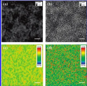
time-resolved PL can only be used when two components are mixed homogenously within the BHJ films. To examine how the exciton lifetime distribution and its related morphology influ-enced the device performance, we performed an analysis of the 2D nanoscale morphology related to the exciton lifetime by combining confocal optical microscopy with a fluorescence module. Figure 2 displays transmitted and exciton lifetime images of rapidly and slowly grown BHJ films. For the rapidly grown film, the transmitted images of the BHJ films reveal uniform and featureless characteristics throughout the structure (Figure 2a), indicating that PCPDTTBT and PCBM were mixed well within the films. Moreover, the exciton lifetime image of Figure 1. (a) Cyclic voltammogram of a PCPDTTBT film. Inset:
Photographs of the polymer film on the ITO electrode in various coloration states. (b) UV-vis spectrum of PCPDTTBT in DCB (dashed line) and in the solid state (solid line); PL in the solid state (0); PL quenching for the PCPDTTBT:PCBM blending film (1:1) (O).
Figure 2. (a, b) Transmitted and (c, d) exciton lifetime images of the
BHJ film prepared by using the rapid and slow growth methods, measured after excitation at 470 nm with a picosecond laser microscope (512× 512 pixels). Scale bars: 2 µm.
the rapidly grown film also reveals an extremely homogeneous lifetime distribution (Figure 2c), in good agreement with the transmitted images. For comparison, the transmitted image of the slowly grown film reveals many bright and dark domains (Figure 2b). Because contrast between the phases is related to differences in the degrees of PL emission, the images clearly indicate that the contrast arose from different material composi-tions. The bright domains are emissions from polymer chains that have stacked or aggregated into a bulk cluster; they maintain a certain level of PL intensity because the aggregation of polymer chains expels some PCBM molecules from the PCP-DTTBT domain, leading to a lower level of PL quenching. Furthermore, we observe the long (red regions) and short (blue regions) lifetimes in the PCPDTTBT- and PCBM-rich domains, respectively. Careful observation revealed that the red regions (PCPDTTBT-rich domains) corresponded to the bright spots in Figure 2b. A slow rate of solvent evaporation facilitated the growth of highly crystalline PCPDTTBT; therefore, some of the PCBM molecules were gradually expelled from the DTTBT domains during the formation of crystalline PCP-DTTBT, resulting in the existence of PCPDTTBT- and PCBM-rich domains. We suspect that these polymer and PCBM domains were continuous from the bottom to the top of the film, thereby forming percolating pathways that favored charge transport.
Although the spatial resolution of confocal optical microscopy depends on the laser wavelength applied (ca. 400-500 nm), the resolution of the time scale can reach the picosecond regime. Therefore, we still can investigate the lifetime distribution on the nanoscale by combining the spatial and temporal signals.32
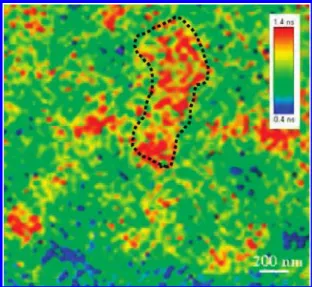
Figure 3 displays an expanded view of the lifetime image of the slowly grown film. The image reveals an extensive green network distributed over the film. We assign this green region to a well-mixed zone of PCPDTTBT and PCBM having a feature size of 30-50 nm. This green network provides a large interfacial area for exciton dissociation, subsequently leading to charge separation. The generated charges could then be transported through the blue regions (for electrons) and the yellow or red regions (for holes) to their respective electrodes. The blue (PCBM-rich) and yellow (PCPDTTBT-rich) regions possessed feature sizes similar to those in the green network. Furthermore, we noted the presence of some red regions having features of much larger size (200-300 nm) near the yellow channel. These red regions, which exhibited much longer exciton
lifetimes, resulted from the highly crystalline PCPDTTBT originating from several polymer chains. Much work has shown similar results for P3HT:PCBM films.33–35A slow rate of solvent
evaporation facilitates the growth of highly crystalline P3HT; therefore, a portion of the PCBM molecules were gradually expelled from the P3HT domains during the formation of crystalline P3HT, resulting in the formation of P3HT- and PCBM-rich domains.
The rapid removal of solvent favors a uniform P3HT:PCBM distribution and prevents the formation of highly ordered lamellae by disrupting the interchain interactions between P3HT chains. Upon solvent annealing, the crystallinity of P3HT:PCBM blend films can be enhanced to provide many visible fibrillar domains of P3HT.36–38It is believed that these fibrillar features
can create percolating paths across the entire film, thereby allowing photogenerated charge to be transported to the relative electrodes. To investigate the effect of solvent annealing on the morphology of PCPDTTBT/PCBM blends, we recorded the topographies of the polymer blends, using AFM in the tapping mode. Figure 4 displays the heights and corresponding phase images of composite PCPDTTBT/PCBM films cast from DCB. From the images for a 10× 10 µm2surface area, we observe
that the slowly grown film based on PCPDTTBT formed coarse chainlike domains having a size of 200-300 nm, which is consistent with the length of a stack of several polymer chains. With its tightly packed polymer chains, the slowly grown film was much rougher than the rapidly grown film (root-mean-square roughnesses of 6.7 and 2.2 nm, respectively). Panels c and d of Figure 4 present expanded views (scan size: 1× 1 µm2) of the images in panels a and b of Figure 4, respectively;
they indicate that the slowly grown films possessed many nanospheres distributed uniformly over the surface. The phase images in Figure 4f reveal a reproducible phase contrast. Because phase contrast is related to differences in the mechanical properties (adhesion and stiffness) of materials, the images clearly indicate that the nanoparticles and valleys were of different chemical nature. The sizes of the nanospheres ranged from 20 to 50 nm, consistent with a polymer possessing a coil structure. A slow solvent evaporation rate generally causes polymers to aggregate to form well-dispersed nanoparticles.39–43
Therefore, we suspect that some of the PCBM molecules were gradually expelled from the PCPDTTBT domains during the slow solvent evaporation process. In this case, we believe that local nanoscale organization created suitable interpenetrating networks for charge transport. In comparison, the rapidly grown film exhibited a uniform mixing of its constituents with unobservable phase contrast. Although a well-mixed blend phase would provide a large interface for electron/hole dissociation, such a uniform phase would be quite unfavorable for the dissociated charge to transport to the electrodes.
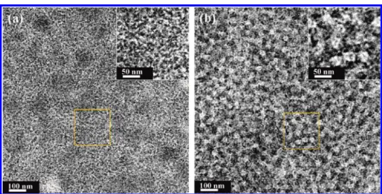
We used TEM to investigate thin freestanding films of PCPDTTBT:PCBM blends (50 wt %) prepared using the rapid and slow growth methods (Figure 5). The darker regions represented nanocrystalline PCBM domains having higher density than that of the polymer. The rapidly grown film (Figure 5a) featured many CPDTTB fibers located all over the film. Upon solvent annealing, much coarser and longer PCPDTTBT crystals formed through the stacking of several fine fibrillar PCPDTTBT units (Figure 5b); moreover, larger PCBM domains had also developed. The expanded image in Figure 5b reveals that the larger PCPDTTBT crystals connected together to form spheres having sizes in the range from 30 to 60 nm, in good agreement with the AFM data. The crystallinity of PCPDTTBT was improved after solvent annealing; the degree of demixing Figure 3. Exciton lifetime images of the slowly grown film. Scale
bars: 200 nm.
of the two components increased, but large-scale phase separa-tion did not occur. As a result, we would expect the charge transport properties to improve for both types of charges as a result of the expansion of the crystalline domains.
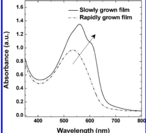
Figure 6 presents the measured optical densities of the slowly and rapidly grown films. The absorption in the red region of the slowly grown film was much stronger than that of the rapidly grown film. For the rapidly grown film, the absorbance peak was located at 535 nm. After solvent annealing, λmaxunderwent
a red-shift to 560 nm, and a visible shoulder appeared at 610 nm. The significant red-shift in absorbance was evidence of a more highly crystalline polymer being induced through solvent annealing, leading to enhanced interchain interactions, which resulted in more delocalized conjugated π electrons and a lowering of the bandgap between the π and π* orbitals.
To investigate the effect of solvent annealing on pristine PCPDTTBT, we measured its field-effect mobilities in top-contact FETs. Figure 7 displays the output and transfer characteristics of PCPDTTBT-based FETs fabricated by using both the rapid- and slow-growth methods. We calculated the field-effect mobility of each transistor in the saturation regime (VDS) -60 V) by plotting the square root of the drain current
against the gate voltage and fitting the data to the following equation:
IDS) WCi
2Lµ(VGS- VT) 2
with values of Ci, W, and L of 1.0× 10⁻⁸F cm-2, 2 mm, and
100 mm, respectively. The field-effect mobilities varied sig-Figure 4. AFM images of polymer active layers. Height images for (a, c) rapidly and (b, d) slowly grown films. Phase images for (e) rapidly and
(f) slowly grown films.
nificantly depending on the evaporation rate of the solvent. The hole mobilities (up to 2.5× 10⁻³cm2V-1s-1) and on/off ratios
(up to 7× 10⁴) of the slowly grown PCPDTTBT were higher
(by 1 order of magnitude) than those of the rapidly grown sample. Because the PCPDTTBT samples had the same mo-lecular weight, the higher mobility of the slowly grown material must have been due to tighter stacking in its polymer film. Even though we did not observe an obvious chain-like feature for the slowly grown film in the AFM images, the PCPDTTBT chains do self-organize into an ordered structure under the surface leading to higher field-effect mobility.
Figure 8 presents the current-voltage (J-V) curves and EQEs for the solar cells incorporating PCPDTTBT and PCBM. We controlled the solvent evaporation rate to investigate the effect of solvent annealing on the cell performance. The short circuit current (JSC) and fill factor (FF) of the device fabricated with
solvent annealing were 7.1 mA cm-2and 61.6%, respectively. These values are both much higher than those exhibited by the rapidly grown film (JSC ) 4.1 mA cm-2; FF ) 36.7%). One
reason for the significantly higher value of JSCof the former is
its superior absorption (see Figure 2), leading to a superior EQE. As indicated in the inset, the spectral response of the PCP-DTTBT-based device featured contributions from the EQE in the wavelength range between 710 and 340 nm. The maximum EQE for the device prepared from the rapidly grown film was 28% at a wavelength of 560 nm. In contrast, for the device incorporating the slowly grown film, the EQE maximum increased to ca. 55% at 560 nm. In addition to a desirable absorption, the morphology of the blend film also plays an important role in affecting device performance. We found that superior percolating pathways and enhanced crystallinity were created in the PCPDTTBT and PCBM blend for the slowly grown film, as evidenced by the exciton liftetime and the AFM and TEM images. We believe that a favorable morphology promoted charge transport, leading to higher values of JSC.
Therefore, we calculated the electron and hole mobilities from the space-charge limited current (SCLC),44using the equation
J ) 9ε0εrµV2/8L3
where ε0εris the permittivity of the polymer, µ is the carrier
mobility, and L is the device thickness. For the rapidly grown Figure 6. Effect of film growth rate on the absorbance of the polymer
film.
Figure 7. Output at different gate voltages (VG) and transfer characteristics in the saturation regime at constant source-drain voltage (VDS) -60
V) for FETs incorporating the (a, b) rapidly and (c, d) slowly grown films.
film, the electron and hole mobilities were 5.4× 10⁻⁸and 3.2 × 10⁻⁹m2V-1 s-1, respectively. For the slowly grown film,
the electron and hole mobilities both increased, to 2.3× 10⁻⁷ and 1.1× 10⁻⁷m2V-1s-1, respectively (the fitted curves can
be found in the Supporting Information). Because the ratio of the electron and hole mobilities was close to unity (1.70), we infer that the presence of bicontinuous transport pathways within the entire active layer and the stronger crystallinity of the blend not only enhanced the charge transport but also balanced the charge mobility. When charge transport in a device is unbal-anced (i.e., hole mobility is significantly less than electron mobility), electron accumulation occurs and the photocurrent is space-charge limited. Under a situation of balanced charge transport, the current is not limited by space-charge effects and a high FF is possible. This phenomenon explains the greater FF of the slowly grown device. Furthermore, the value of VOC
of the PCPDTTBT-based device (0.7 V) was greater than that of the P3HT-based cell, by 0.1 V. The higher value of VOCfor
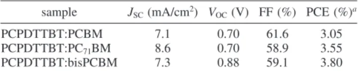
the copolymer-containing device is consistent with its lower HOMO energy level. Combing these parameters, the device fabricated through solvent annealing provided a PCE of 3.05%. The PCE of PCPDTTBT-based devices was enhanced further when using 6,6-phenyl-C71-butyric acid methyl ester (PC71BM)
or bisPCBM in place of PCBM. Table 1 summarizes the output characteristics of the various PCPDTTBT-based devices, which were fabricated by using the slow growth method. The value of JSCincreased from 7.1 to 8.6 mA cm-2after replacing PCBM
with PC71BM; VOCincreased from 0.7 to 0.88 V after replacing
PCBM with bisPCBM; in each case, the other parameters remained almost constant. This behavior resulted from the larger absorbance of PC71BM45–48and the higher LUMO energy level
of bisPCBM49 relative to those of PCBM. Thus, the devices
based on PC71BM and bisPCBM delivered PCEs of 3.55% and
3.80%, respectively.
4. Conclusion
We have investigated the correlation between the exciton lifetime distribution and the morphology of PCPDTTBT:PCBM blends. The morphologies of the solvent-annealed PCPDTTBT: PCBM blends exhibited two important features that resulted in efficient solar cells. First, exciton lifetime images revealed that PCPDTTBT- and PCBM-rich domains were formed within the blend films during the self-organization process. Second, the demixing between the two components led to bicontinuous pathways, having a feature size (width) of 30-50 nm, for charge transport; here, the exciton lifetime images were consistent with the TEM images. A PCPDTTBT/bisPCBM-based solar cell prepared through solvent annealing exhibited a PCE of 3.8% under AM 1.5 G (100 mW cm-2) illumination.
Acknowledgment. The authors are grateful to the National Science Council (NSC), Taiwan (NSC 98-2221-E-001-002), and Academia Sinica for financial support.
Supporting Information Available: Figure S1 showing the measured J-V characteristics under dark for hole-only and electron-only PV devices consisting of PCPDTBT /PCBM active layer grown at rapidly and slowly grown rates. This material is available free of charge via the Internet at http://pubs.acs.org.
References and Notes
(1) Yu, G.; Gao, J.; Hummelen, J. C.; Wudl, F.; Heeger, A. J. Science
1995, 270, 1789.
(2) Halls, J. J. M.; Friend, R. H. Synth. Met. 1997, 85, 1307. (3) Hou, J.; Chen, H. Y.; Zhang, S.; Yang, Y. J. Phys. Chem. C 2009,
113, 21202.
(4) Liang, Y.; Feng, D.; Wu, Y.; Tsai, S. T.; Li, G.; Ray, C.; Yu, L.
J. Am. Chem. Soc. 2009, 131, 7792.
(5) Blouin, N.; Michaud, A.; Gendron, D.; Wakim, S.; Blair, E.; Neagu-Plesu, R.; Belleteˆte, M.; Durocher, G.; Tao, Y.; Leclerc, M. J. Am. Chem.
Soc. 2008, 130, 732.
(6) Liang, Y.; Feng, D.; Guo, J.; Szarko, J. M.; Ray, C.; Chen, L. X.; Yu, L. Macromolecules 2009, 42, 1091.
(7) Hou, J.; Chen, T. L.; Zhang, S.; Chen, H. Y.; Yang, Y. J. Phys.
Chem. C 2009, 113, 1601.
(8) Becerril, H. A.; Miyaki, N.; Tang, M. L.; Mondal, R.; Sun, Y. S.; Mayer, A. C.; Parmer, J. E.; McGehee, M. D.; Bao, Z. J. Mater. Chem.
2009, 19, 591.
(9) Subbiah, J.; Beaujuge, P. M.; Choudhury, K. R.; Ellinger, S.; Reynolds, J. R.; So, F. ACS Appl. Mater. Interfaces 2009, 1, 1154.
(10) Lindgren, L. J.; Zhang, F.; Andersson, M.; Barrau, S.; Hellstro¨m, S.; Mammo, W.; Perzon, E.; Ingana¨s, O.; Andersson, M. R. Chem. Mater.
2009, 21, 3491.
(11) Zhang, Y.; Yip, H. L.; Acton, O.; Hau, S. K.; Huang, F.; Jen, A. K. Y. Chem. Mater. 2009, 21, 2598.
(12) Mu¨hlbacher, D.; Scharber, M.; Morana, M.; Zhu, Z.; Waller, D.; Gaudiana, R.; Brabec, C. AdV. Mater. 2006, 18, 2884.
(13) Hou, J.; Chen, H. Y.; Zhang, S.; Li, G.; Yang, Y. J. Am. Chem.
Soc. 2008, 130, 16144.
(14) Zhang, M.; Tsao, H. N.; Pisula, W.; Yang, C.; Mishra, A. K.; Mu¨llen, K. J. Am. Chem. Soc. 2007, 129, 3472.
(15) Berlin, A.; Brenna, E.; Pagani, G. A.; Sannicolo, F. Synth. Met.
1992, 51, 287.
(16) Peet, J.; Kim, J. Y.; Coates, N. E.; Ma, W. L.; Moses, D.; Heeger, A. J.; Bazan, G. C. Nat. Mater. 2007, 6, 497.
(17) Andersson, B. V.; Herland, A.; Masich, S.; Ingana¨s, O. Nano Lett.
2009, 9, 853.
(18) Moon, J. S.; Lee, J. K.; Cho, S.; Byun, J.; Heeger, A. J. Nano Lett.
2009, 9, 230.
(19) Yu, B. Y.; Lin, W. C.; Huang, J. H.; Chu, C. W.; Lin, Y. C.; Kuo, C. H.; Lee, S. H.; Wong, K. T.; Ho, K. C.; Shyue, J. J. Anal. Chem. 2009,
81, 8936.
(20) van Bavel, S.; Sourty, E.; de With, G.; Veenstra, S.; Loos, J. J.
Mater. Chem. 2009, 19, 5388.
(21) Li, G.; Shrotriya, V.; Huang, J.; Yao, Y.; Moriarty, T.; Emery, K.; Yang, Y. Nat. Mater. 2005, 4, 864.
(22) Li, G.; Yao, Y.; Yang, H.; Shrotriya, V.; Yang, G.; Yang, Y. AdV.
Funct. Mater. 2007, 17, 1636.
Figure 8. J-V characteristics under illumination at 100 mW cm-2
(simulated AM 1.5G) of photovoltaic devices incorporating active layers prepared by using two different growth rates. Inset: EQE spectra of devices incorporating the rapidly and slowly grown films.
TABLE 1: Photovoltaic Parameters for BHJ Devices Based on PCPDTTBT and Fullerene Derivatives
sample JSC(mA/cm2) VOC(V) FF (%) PCE (%)a
PCPDTTBT:PCBM 7.1 0.70 61.6 3.05 PCPDTTBT:PC71BM 8.6 0.70 58.9 3.55
PCPDTTBT:bisPCBM 7.3 0.88 59.1 3.80
a
Active layer with the weight ratio of PCPDTTBT:fullerene) 1:2 (w/w).
(23) Lee, J. K.; Ma, W. L.; Brabec, C. J.; Yuen, J.; Moon, J. S.; Kim, J. Y.; Lee, K.; Bazan, G. C.; Heeger, A. J. J. Am. Chem. Soc. 2008, 130, 3619.
(24) Chen, H. Y.; Yang, H.; Yang, G.; Sista, S.; Zadoyan, R.; Li, G.; Yang, Y. J. Phys. Chem. C 2009, 113, 7946.
(25) Lin, H. C.; Lee, K. W.; Tsai, C. M.; Wei, K. H. Macromolecules
2006, 39, 3808.
(26) Lucas, P.; El Mehdi, N.; AnhHo, H.; Belanger, D.; Breau, L.
Synthesis 2000, 9, 1253.
(27) Li, K. C.; Huang, J. H.; Hsu, Y. C.; Huang, P. J.; Chu, C. W.; Lin, J. T.; Ho, K. C.; Lin, K. C. Macromolecules 2009, 42, 3681.
(28) Janietz, S.; Bradley, D. D. C.; Grelly, M.; Giebeler, C.; Inbasekaran, M.; Woo, E. P. Appl. Phys. Lett. 1998, 73, 2453.
(29) Scharber, M. C.; Mu¨hlbacher, D.; Koppe, M.; Denk, P.; Waldauf, C.; Heeger, A. J.; Brabec, C. J. AdV. Mater. 2006, 18, 789.
(30) Veldman, D.; Ipek, O¨ .; Meskers, S. C. J.; Sweelssen, J.; Koetse, M. M.; Veenstra, S. C.; Kroon, J. M.; van Bavel, S. S.; Loos, J.; Janssen, R. A. J. J. Am. Chem. Soc. 2008, 130, 7721.
(31) Lin, Y. Y.; Chen, C. W.; Chu, T. H.; Su, W. F.; Lin, C. C.; Ku, C. H.; Wub, J. J.; Chen, C. H. J. Mater. Chem. 2007, 17, 4571.
(32) Heilemann, M.; Herten, D. P.; Heintzmann, R.; Cremer, C.; Mu¨ller, C.; Tinnefeld, P.; Weston, K. D.; Wolfrum, J.; Sauer, M. Anal. Chem. 2002,
74, 3511.
(33) Park, J. H.; Kim, J. S.; Lee, J. H.; Lee, W. H.; Cho, K. J. Phys.
Chem. C 2009, 113, 17579.
(34) Kim, H.; Shin, M.; Kim, Y. J. Phys. Chem. C 2009, 113, 1620. (35) Huang, J. H.; Chien, F. C.; Chen, P.; Ho, K. C.; Chu, C. W. Anal.
Chem. 2010, 82, 1669.
(36) Chang, J. F.; Sun, B.; Breiby, D. W.; Nielsen, M. M.; So¨lling, T. I.; Giles, M.; McCulloch, I.; Sirringhaus, H. Chem. Mater. 2004, 16, 4772. (37) Quiles, M. C.; Ferenczi, T.; Agostinelli, T.; Etchegoin, P. G.; Kim, Y.; Anthopoulos, T. D.; Stavrinou, P. N.; Bradley, D. D. C.; Nelson, J.
Nat. Mater. 2008, 7, 158.
(38) Hoppe, H.; Sariciftci, N. S. J. Mater. Chem. 2006, 16, 45. (39) Huang, J. H.; Yang, C. Y.; Ho, Z. Y.; Kekuda, D.; Wu, M. C.; Chien, F. C.; Chen, P.; Chu, C. W.; Ho, K. C. Org. Electron. 2009, 10, 27. (40) Huang, J. H.; Ho, Z. Y.; Kekuda, D.; Chang, Y.; Chu, C. W.; Ho, K. C. Nanotechnology 2009, 20, 025202.
(41) Huang, J. H.; Kekuda, D.; Chu, C. W.; Ho, K. C. J. Mater. Chem.
2009, 19, 3704.
(42) Gill, W. D. J. Appl. Phys. 1972, 43, 5033.
(43) Yu, J.; Wu, C.; Sahu, S. P.; Fernando, L. P.; Szymanski, C.; McNeill, J. J. Am. Chem. Soc. 2009, 131, 18410.
(44) Melzer, C.; Koop, E. J.; Mihailetchi, V. D.; Blom, P. W. M. AdV.
Funct. Mater. 2004, 14, 865.
(45) Wienk, M. M.; Kroon, J. M.; Verhees, W. J. H.; Knol, J.; Hummelen, J. C.; van Hal, A. P.; Janssen, R. A. J. Angew. Chem., Int. Ed.
2003, 42, 3371.
(46) Wang, X. J.; Perzon, E.; Oswald, F.; Langa, F.; Admassie, A.; Andersson, M. R.; Ingana¨s, O. AdV. Funct. Mater. 2005, 15, 1665.
(47) Yao, Y.; Shi, C. J.; Li, G.; Shrotriya, V.; Pei, Q. B.; Yang, Y.
Appl. Phys. Lett. 2006, 89, 153507–1.
(48) Huang, J. H.; Li, K. C.; Kekuda, D.; Padhy, H. H.; Lin, H. C.; Ho, K. C.; Chu, C. W. J. Mater. Chem. 2010, 20, 3295.
(49) Lenes, M.; Wetzelaer, G. A. H.; Kooistra, F. B.; Veenstra, S. C.; Hummelen, J. C.; Blom, P. W. M. AdV. Mater. 2008, 20, 2116. JP9120639