Formation and nonvolatile memory characteristics of W nanocrystals by in-situ
steam generation oxidation
Shih-Cheng Chen
a, Ting-Chang Chang
b,⁎
, Chieh-Ming Hsieh
c, Hung-Wei Li
d, S.M. Sze
c, Wen-Ping Nien
e,
Chia-Wei Chan
e, Fon-Shan Yeh(Huang)
a, Ya-Hsiang Tai
fa
Department of Electrical Engineering and Institute of Electronic Engineering, National Tsing Hua University, Taiwan
b
Department of Physics and Center for Nanoscience and Nanotechnology, National Sun Yat-Sen University Taiwan, ROC
c
Institute of Electronics, National Chiao Tung University, Taiwan, HsinChu, 300 Taiwan, ROC
d
Department of Photonics and Institute of Electro-Optical Engineering, National Chiao Tung University, Hsinchu, Taiwan, ROC
eProMOS Technologies, No. 19 Li Hsin Rd., Science-Based Industrial Park, Hsinchu, 300 Taiwan, ROC f
Department of Photonics and Display Institute, National Chiao Tung University, Hsinchu, Taiwan, ROC
a b s t r a c t
a r t i c l e i n f o
Available online 7 September 2010 Keywords:
Tungsten
Nonvolatile memory Nanocrystals In-situ stem generation
The authors provide the formation and memory effects of W nanocrystals nonvolatile memory in this study. The charge trapping layer of stacked a-Si and WSi2was deposited by low pressure chemical vapor deposition (LPCVD) and was oxidized by in-situ steam generation system to form uniform W nanocrystals embedded in SiO2. Transmission electron microscopy analyses revealed the microstructure in the thin film and X-ray photon-emission spectra indicated the variation of chemical composition under different oxidizing conditions. Electrical measurement analyses showed the different charge storage effects because the different oxidizing conditions influence composition of trapping layer and surrounding oxide quality. Moreover, the data retention and endurance characteristics of the formed W nanocrystal memory devices were compared and studied. The results show that the reliability of the structure with 2% hydrogen and 98% oxygen at 950 °C oxidizing condition has the best performance among the samples.
© 2010 Elsevier B.V. All rights reserved.
1. Introduction
The conventional nonvolatile memory (NVM, flash memory) suffers some limitations for continual scaling of device structures. Nanocrystal nonvolatile memory devices have been investigated to overcome the drawbacks of the conventionalfloating gate memory in recently years due to the discrete traps storage mode as the charge center[1–6]. In nanocrystal nonvolatile memory devices, the density of nanocrystals for nanoscale devices is an issue because the memory window is dependent on its density and high density is helpful to scaling down of devices structure. When the density of nanocrystals is very high, the quality of surrounding oxide of nanocrystals is a critical problem. The electron storing in nanocrystals will escape by trap to trap tunneling[7,8].
According to the values of other literatures, the in-situ steam generation (ISSG) oxidation process can be used to improve the quality of thin oxide. It has a faster oxidation rate than dry or RTO oxidation due to more oxygen radicals produced by introducing some hydrogen. Because of its quick oxidation rate, ISSG provides excellent quality of thin oxide and many references have demonstrated that ISSG oxide
shows a much better reliability property than dry or RTO oxide[9–12]. Therefore, we apply ISSG to fabricate our tungsten nanocrystals nonvolatile memory in this work. The applications are on the tunneling oxide fabrication and nanocrystals formation, respectively.
2. Experiment
In this work the tungsten nanocrystal NVM capacitor structure was fabricated on a single-crystal 8 in. (100) oriented P-type silicon.Fig. 1
exhibits the processflow and cross-sectional structure. After standard Radio Corporation of America (RCA) process, a 5-nm-thick SiO2layer
as a tunnel oxide was formed by an in-situ steam generation (ISSG) oxidation process. The hydrogen content of (O2+ H2) gases were kept
at 2%. A 4-nm-thick tungsten silicide (WSi2) thinfilm was deposited
onto the tunnel oxide by low pressure chemical vapor deposition (LPCVD) system flowing in WF6 and SiH4 at room temperature.
Subsequently, a 6-nm-thick amorphous silicon (a-Si) was deposited by the same system justflowing in SiH4. After depositing a-Si/WSi2
double layer structure, an in-situ steam generation oxidation process was utilized at 850 °C (sample A) and 950 °C (sample B) with 60 s to make the WSi2layer precipitate tungsten nanocrystals which were
embedded between the tunnel oxide and the control oxide. Afterward, a 50-nm-thick SiO2was deposited by plasma enhanced
chemical vapor deposition (PECVD) system to form a thicker control
Thin Solid Films 519 (2010) 1677–1680
⁎ Corresponding author.
E-mail address:[email protected](T.-C. Chang).
0040-6090/$– see front matter © 2010 Elsevier B.V. All rights reserved. doi:10.1016/j.tsf.2010.08.167
Contents lists available atScienceDirect
Thin Solid Films
oxide layer. 5μm aluminum metal electrodes were deposited on the device at both sides to form a metal/oxide/isolated nanocrystal/oxide/ silicon structure by thermal vapor deposition coating. Electrical characteristics of the capacitance–voltage (C–V) hysteresis were also measured by HP4284 Precision LCR Meter with a high frequency of 100 kHz. Transmission electron microscope (TEM) analysis and X-ray
photoelectron spectroscopy (XPS) were adopted for microstructure and chemical material analysis of nanocrystals.
3. Discussion and results
Fig. 2(a) and (b) shows the cross-sectional TEM images of sample
A and sample B structures, respectively. InFig. 2(a) it can be observed that even through oxidizing at 850 °C the almost WSi2trapping layer
still seemed to be a continuous layer and tungsten nanocrystals were seldom formed. However, the continuous WSi2trapping layer have
been formed by the discrete W nanocrystals after oxidizing at 950 °C as shown inFig. 2(b). From TEM image analysis the average diameter of W nanocrystals of sample B is approximately 8 nm. Therefore, we think that the critical temperature of oxidizing WSi2to form complete
W nanocrystals by using an ISSG system is 950 °C.
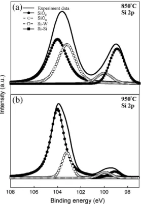
To further analyze the chemical state of NCs, we have performed XPS analysis by using an Al Kα (1486.6 eV) X-ray radiation to assay the chemical compositions.Figs. 3 and 4exhibit the W 4f and Si 2p XPS spectra of different oxidation temperature conditions. FromFig. 3
(a), it can be found that this spectrum has two main peaks which represent W 4f7/2and 4f5/2binding energies, respectively. It can be
thought that each of these two main peaks is composed of two sub-peaks W–W bonds and W–Si bonds. The binding energies for W–W bond are 31.4 eV (4f7/2) and 33.5 eV (4f5/2), and W–Si binding
energies are 30.8 eV (4f7/2) and 32.9 eV (4f5/2), respectively[13,14].
As the oxidation temperature is increasing the peak intensity of W–W bond increase and W–Si decrease as shown inFig. 3(b). It indicates that the broken W–Si bond and W connect each other to form W nanocrystals and Si was oxidized to form SiO2. The tendency for the
peak intensity of W–Si bond is opposite to that of W–W bond when the temperature gets higher.
InFig. 4(a), there are two main peaks in the Si 2p spectrum. One is composed of the peaks for SiO2and SiOx binding energy located at
104 eV and 103.2 eV. The Si–W (100 eV) and Si–Si (99.2 eV) sub-peaks constitute the other main peak[13,14]. From the analysis of the XPS Si 2p spectrum, the Si, WSi, and SiOx peaks decrease and SiO2
increases as oxidation temperature increase from 850 °C to 950 °C as Fig. 1. Processflow and tungsten nanocrystal NVM structure.
Fig. 2. TEM diagram of tungsten-dot NVMs (a) oxidation at 850 °C and (b) oxidation at 950 °C.
Fig. 3. XPS analysis of the W 4f core-level spectrum (a) oxidation at 850 °C and (b) oxidation at 950 °C.
shown inFig. 4(b). It implies that Si can be oxidized to SiO2and the
SiO2quality is better when the oxidation temperature is 950 °C than
850 °C due to its high thermal energy. That is the reason why a nearly continuousfilm and nanocrystals in different oxidation conditions were observed from TEM.
In our previous study, the possible presence of the tungsten oxide on a very similar material is demonstrated[15]. However the tungsten oxide signal is absent inFig. 3. The enthalpies (−△H) of W–O and Si–O at room temperature are−672.0 and −799.6 KJ mol−1. Because the
enthalpy of Si–O is higher than with W–O, the reaction between oxygen radicals and Si atoms is easier than that between oxygen radicals and W atoms during the thermal oxidation process. It indicated that bonding of Si–O is more stable than W–O. Thereby oxygen will oxidize Si first. From
Fig. 4, it can be observed that a part of Si was not oxidized in this work. Thus, it is considered that the amount of oxygen is not enough to oxidize Si completely. It is the reason that the tungsten oxide signal was not observed.
The basic C–V hysteresis diagram electrical characteristics of oxidation at 850 °C (sample A) and 950 °C (sample B) with 60 s devices are shown inFig. 5. Under the ±10 V comparing toflat-band gate voltage operation, the memory window of samples A (solid circle) and B (solid square) is 1.8 V and 9 V, respectively. From TEM
analysis and C–V measuring results, it is considered that the more large memory window in oxidation at 950 °C than 850 °C is contributed by W nanocrystals being completely formed by oxidizing at 950 °C due to its high thermal energy. Moreover, the hysteresis loops follow the counterclockwise direction due to injection of electrons from the inversion state and discharge of electrons from the accumulation state of Si substrate.
Fig. 6presents the room temperature retention characteristics of
samples A and B. FromFig. 6, we used an extrapolation to give a long-term predictable result (solid and dotted line) after 1000 s (stable region of retention)[16]. The memory window significantly decays during thefirst 100 s due to charge emission from the shallow traps in SiOx matrix to the substrate. However, after 100 s the memory Fig. 4. XPS analysis of the Si 2p core-level spectrum (a) oxidation at 850 °C and
(b) oxidation at 950 °C.
Fig. 5. Electrical characteristics of C–V hysteresis under ±10 V gate voltage operation.
Fig. 6. Retention of the tungsten nanocrystal NVMs.
Fig. 7. Endurance characteristic of tungsten nanocrystal NVMs under the pulse conditions of VG-VFB = ± 10 V for 1 ms (a) oxidation at 850 °C and (b) oxidation at 950 °C. Theflat-band voltage can be defined by using the C–V hysteresis.
1679 S.-C. Chen et al. / Thin Solid Films 519 (2010) 1677–1680
window is more stable. After 104s the memory window charge of
samples A and B remained of 14% and 42%, respectively. As expected, the retention property of sample B is better because the surrounding SiO2 quality of oxidation at 950 °C is better than 850 °C. That is
confirmed from XPS analysis.
Fig. 7shows the endurance characteristic of samples A and B under
pulse condition of VG-VFB = ± 10 V for 1 ms. Theflat-band voltage can be defined by using the C–V hysteresis under ±10 V gate voltage operation. The memory of sample A can be distinguished after 106 program/erase cycles at room temperature and the memory is not apparently degradable, but the variation offlat-band voltage is not stable asFig. 7(a) shows. However, it is found that the variations of the memory window andflat-band voltage are very stable after a 106
program/erase for sample B from Fig. 7(b). The stable flat-band voltage and excellent endurance property are due to the contribution of good quality of surrounding oxide and tunneling oxide.
4. Conclusions
In conclusion, the ISSG system was used to oxidize WSi to precipitate tungsten nanocrystals embedded in SiO2as a nonvolatile memory. The
critical temperature to oxidize WSi to form complete W nanocrystals by using ISSG oxidation process is 950 °C. By using ISSG oxidation process it can improve the quality of thin oxide greatly and therefore we can gain superior retention and endurance properties. In sample B a larger memory window of 9 V was observed after ±10 V voltage sweep for nonvolatile memory application due to the tungsten nanocrystals formed completely. The date retention of the nanocrystal memory device is also good enough to maintain for 10 years and the endurance property can over 106program/erase operation.
Acknowledgements
This work was performed at the National Science Council Core Facilities Laboratory for Nanoscience and Nanotechnology in the
Kaohsiung–Pingtung area and was supported by the National Science Council of the Republic of China under Contract Nos. NSC-97-3114-M-110-001 and NSC 97-2112-M-110-009-MY3.
Reference
[1] H.E. Maes, J. Witter, G. Groeseneken, Proc. 17 European Solid State Devices Res. Conf. Bologna 1987, 1998, p. 157.
[2] S. Tiwari, F. Rana, K. Chan, H. Hanafi, C. Wei, D. Buchanan, IEEE Int. Electron Devices Meet. Tech. Dig. (1995) 521.
[3] Chao-Cheng Lin, Ting-Chang Chang, Chun-Hao Tu, Shih-Ching Chen, Chih-Wei Hu, Simon M. Sze, Tseung-Yuen Tseng, Sheng-Chi Chen, Jian-Yang Lin, J. Phys. D Appl. Phys. 43 (2010) 075106 (4pp).
[4] Chao-Cheng Lin, Ting-Chang Chang, Chun-Hao Tu, Wei-Ren Chen, Chih-Wei Hu, Simon M. Sze, Tseung-Yuen Tseng, Sheng-Chi Chen, Jian-Yang Lin, Appl. Phys. Lett. 93 (2008) 222101.
[5] Wei-Ren Chen, Ting-Chang Chang, Jui-Lung Yeh, S.M. Sze, Chun-Yen Chang, J. Appl. Phys. 104 (2008) 094303.
[6] Wei-Ren Chen, Ting-Chang Chang, Jui-Lung Yeh, S.M. Sze, Chun-Yen Chang, Appl. Phys. Lett. 92 (2008) 152114.
[7] M. Houssa, M. Tuominen, M. Naili, V. Afanas'ev, A. Stesmans, S. Haukka, M.M. Heyns, J. Appl. Phys. 87 (2000) 8615.
[8] W.R. Chen, T.C. Chang, P.T. Liu, P.S. Lin, C.H. Tu, C.Y. Chang, Appl. Phys. Lett. 90 (2007) 112108.
[9] T.Y. Luo, M. Laughery, G.A. Brown, Member, IEEE, H.N. Al-Shareef, V.H.C. Watt, A. Karamcheti, M.D. Jackson, and H.R. Huff, IEEE Electron Device Lett., 21 (2000) No. 9, September.
[10] Tung-Ming Panz, Electrochem. Solid-State Lett. 9 (2) (2006) G66.
[11] Naoto Nagai, K. Terada, Y. Muraji, H. Hashimoto, T. Maeda, Y. Maeda, E. Tahara, N. Tokai, A. Hatta, J. Appl. Phys. 91 (2002) 7.
[12] F. Roozeboom, J.C. Gelpey, M.C. Ozturk, J. Nakos, PV 99–10 Advances in rapid thermal processing: proceedings of the symposium (1999).
[13] K. Akimoto, Appl. Phys. Lett. 41 (1) (1978).
[14] C.M. Lin, J.S. Chen, Electrochem. Solid-State Lett. 11 (4) (2008) H99.
[15] Shih-Cheng Chen, Ting-Chang Chang, Wei-Ren Chen, Yuan-Chun Lo, Kai-Ting Wu, S.M. Sze, Jason Chen, I.H. Liao, Fon-Shan Yeh(Huang), Thin Solid Films 518 (2010) 7339.
[16] W.R. Chen, T.C. Chang, P.T. Liu, J.L. Yen, C.H. Tu, J.C. Lou, C.F. Yeh, C.Y. Chang, Appl. Phys. Lett. 91 (2007) 082103.