The effect of a concentration gradient on interfacial reactions
in microbumps of Ni/SnAg/Cu during liquid-state soldering
Y.S. Huang,
aH.Y. Hsiao,
aChih Chen
a,⇑and K.N. Tu
ba
Department of Materials Science and Engineering, National Chiao Tung University, Hsinchu 30010, Taiwan, ROC
b
Department of Materials Science and Engineering, University of California at Los Angeles, Los Angeles, CA 90095-1595, USA
Received 1 November 2011; revised 21 January 2012; accepted 23 January 2012 Available online 28 January 2012
We report new findings in Ni/SnAg–solder/Cu microbumps having a reduced solder thickness in the range of 40–10 lm; the growth rate of the intermetallic compounds depends strongly on the solder thickness. In the Ni/40 lm solder/Cu samples, the com-pound which grew on the Ni side grew slightly faster than that on the Cu side. However, the growth reverses as the solder thickness decreases below 20 lm due to the change in Cu and Ni concentration gradients in the solder.
Ó 2012 Acta Materialia Inc. Published by Elsevier Ltd. All rights reserved.
Keywords: Diffusion; Intermetallic compounds; Soldering; Copper; Nickel
The microelectronics industry is currently mak-ing advances in three-dimensional integrated circuit (3-D IC) technology. However, the packaging of 3-(3-D IC is problematic because of metallurgical reactions in microbumps[1]. In the 3-D IC packaging, the diameter of the solder joints can be reduced to 10 lm; this is known as microbumps[2]. The volume of such joints is 1000 times smaller than that of solder joints in flip-chip technology, which have a diameter of 100 lm. At the same time, the contact area is 100 times smaller, but the diffusion or reaction distance is only 10 times less. The reduced size of the microbump has introduced new and challenging yield and reliability concerns, because the temperature and time of processing remains un-changed. A critical concern is the rapid saturation of the concentration of Cu and Ni in the solder due to dis-solution of Cu and Ni from under-bump metallization (UBM), and also the effect of dissolution on the rate of ternary (Cu, Ni)6Sn5intermetallic compound (IMC) for-mation in the solder joint[3–8].
In the literature, several reports have addressed the metallurgical reactions in the Ni/Pb-free solder/Cu sys-tems in flip-chip technology. Wang and Liu[9]and Teng and Liu[10]reported that the IMCs on the Ni side grew faster than those on the Cu side for a solder joint of thickness of 150 lm. Shao et al. [11]also reported that the Cu atoms diffused to the Ni side to form ternary
Cu–Ni–Sn IMCs in a flip-chip solder joint. This is be-cause the flux of Ni atoms to the Cu end is smaller than that of Cu atoms to the Ni end because the solubility of Cu in the solder is higher. Recently, Li et al.[12]studied interfacial reactions in the Cu/10 lm Sn/Cu system and found that the Cu–Sn IMCs grew from both sides at approximately the same rate. The entire Sn layer was transformed into Cu–Sn IMCs after reflowing at 340°C for 40 min. The key finding, as mentioned above, is that the Cu and Ni atoms in the solder can significantly affect the growth of the interfacial IMCs on both sides of the joint. Hence we expect that the effect will be even more serious in the reduced size of microbumps. How-ever, no reports have been published on this subject yet. In this study, we fabricated an Ni/SnAg solder/Cu structures with solder thicknesses of 40, 20 and 10 lm. The samples were reflowed at 260°C for various times. We found that the growth rate of the IMC increases on the Cu side and decreases on the Ni side with decreasing solder thickness. Only the ternary (Cu, Ni)6Sn5 IMC was found. Compositional analysis of the solder and of the IMCs was performed in order to propose a plausible mechanism for this interesting observation.
Figure 1(a) shows a schematic drawing of the sample structure and the bonding setup. The structure consists of two parts. The lower part is fabricated using Si wafer as the substrate, 20 lm Cu as the UBM and of 9, 19 or 60 lm Sn2.3Ag as the solder cap. The upper part is fab-ricated using Si wafer as the substrate, 3 lm electroplated
1359-6462/$ - see front matterÓ 2012 Acta Materialia Inc. Published by Elsevier Ltd. All rights reserved. doi:10.1016/j.scriptamat.2012.01.046
⇑Corresponding author. E-mail:[email protected]
Available online at www.sciencedirect.com
Scripta Materialia 66 (2012) 741–744
Ni as the UBM, and 2 lm Sn2.3Ag as the solder cap.
Figure 1(b) shows the cross-sectional scanning electron microscopy (SEM) image of the upper part of the sam-ple.Figure 1(c)–(e) shows the cross-sectional SEM image of the lower part of the sample. Both parts of the samples were reflowed (the first reflow) at 260°C for 1 min to en-sure the formation of the solder cap and its firm attach-ment to the Cu or Ni. The bonding and reflowing process shown inFigure 1(a) was then carried out. The two parts were aligned, placed in face-to-face contact and reflowed at 260°C for 3 min (the second reflow). By joining the parts in Figure 1(b), (c) and (d) to the part in Figure 1(e), we fabricated the Ni/SnAg/Cu structures with three SnAg solder thicknesses, of 10, 20 and 40 lm, respec-tively. These three samples are denoted as Ni/10 lm sol-der/Cu, Ni/20 lm solsol-der/Cu, and Ni/40 lm solder/Cu in this paper.
The as-bonded samples were further reflowed (the third reflow) at 260°C for 0, 5, 10 and 20 min in order to investigate the growth of IMC on both the Cu/solder and Ni/solder interfaces. Cross-sectional samples were polished and observed using field-emission SEM. The compositions of solder and IMC in the joint were ana-lyzed by field-emission electron probe X-ray microanal-ysis (EPMA), using a JXA-8800M microanalyzer with a resolution of 0.01 at.%.
In this paper, the reflow time represents the total flow time of three reflows, i.e. it includes the 1 min re-flow after the electroplating of the solder, the 3 min reflow during bonding and the additional reflow to grow the IMC. Thus the reflow times under investigation are actually 4, 9, 14 and 24 min.
The growth behavior of interfacial IMCs in the Ni/ 40 lm solder/Cu appears similar to that in the Ni/ 150 lm thick Sn/Cu structure reported in the literature
[9]. Figure 2(a) and (b) shows cross-sectional SEM back-scattered images of the Ni/40 lm solder/Cu sam-ples after reflows at 260°C for 4 and 24 min, respec-tively. The compositional analysis by EPMA indicates that the IMCs grown on both the top and bottom sides are (Cu, Ni)6Sn5. Figure 2(a) shows the cross-sectional SEM image for the Ni/40 lm solder/Cu sample after the 4 min reflow, which is the as-bonded sample. The (Cu, Ni)6Sn5on the Cu side is of the scallop-type, with an average thickness of about 3.48 lm, whereas that on the Ni side is needle-like, with an average thickness of about 1.99 lm. Figure 2(b) shows the microstructures of the Ni/40 lm solder/Cu sample after the 24 min re-flow. The average thickness of the (Cu, Ni)6Sn5on the
Cu side grew to 6.10 lm. The average thickness of the (Cu, Ni)6Sn5on the Ni side grew to 5.58 lm. Some of the IMC on the Ni side spalled into the SnAg solder.
Figure 3 plots the relationship between the thickness of (Cu, Ni)6Sn5and the reflow time of this set of samples (Ni/40 lm solder/Cu), using solid triangular dots. It indicates that the thickness of the (Cu, Ni)6Sn5on the Cu side is slightly thicker than that on the Ni side. How-ever, the slope or the growth rate appears faster for the IMC on the Ni side. The thickness of the IMCs on the Ni side increases from 1.99 to 5.58 lm after the 24 min reflow, whereas it increases from 3.84 to 6.10 lm on the Cu side.
The IMC growth rate changed in the samples with the reduced thickness of solder. Figure 2(c) and (d) shows cross-sectional SEM images of the Ni/20 lm sol-der/Cu samples after reflow at 260°C for 4 and 24 min, respectively. The compositional analysis indicates that the interfacial IMC on both sides are also (Cu, Ni)6Sn5.
Figure 2(c) shows the microstructure of Ni/20 lm sol-der/Cu sample after the 4 min reflow, which is the as-bonded sample. The (Cu, Ni)6Sn5on the Cu side is of the scallop-type, with an average thickness of 3.58 lm, whereas that on the Ni side appears to be needle-like, with an average thickness of 1.57 lm. Compared with the results inFigure 2(a), the thickness of the needle-like (Cu, Ni)6Sn5on the Ni side is thinner than that in the
Figure 2. Cross-sectional SEM images showing the microstructure of the samples. (a) As-bonded with the 40 lm thick solder. (b) Reflow for 24 min with the 40 lm thick solder at 260°C; (c) As-bonded with the 20 lm thick solder. (d) Reflow for 24 min with the 20 lm thick solder at 260°C. (e) As-bonded with the 10 lm thick solder. (f) Reflow for 24 min with the 10 lm thick solder at 260°C.
Figure 1. (a) Schematic diagram of the sample cross-sectional structure and bonding process of the Ni/SnAg/Cu microbumps. Cross-sectional SEM images for (b) 10 lm thick, (c) 19 lm thick and (d) 60 lm thick SnAg solder on 20 lm electroplated Cu UBM. (e) Cross-sectional SEM images for 2 lm thick SnAg solder on 3 lm electroplated Ni UBM.
Ni/40 lm solder/Cu sample after the 4 min reflow. As the reflow time increased, the IMC on the Cu side grew faster than that on the Ni side, as shown in theFigure 2(d). After the 24 min reflow, the average thickness of the (Cu, Ni)6Sn5on the Cu side is 7.59 lm, whereas it is only 3.51 lm on the Ni side.
Figure 3also plots the measured IMC thickness as a function of reflow time of this set of samples (Ni/20 lm solder/Cu), using solid circular dots. The IMC on the Cu side continued to grow thicker as the reflow time in-creased. However, the IMC on the Ni side did not grow obviously after the 9 min reflow, with the average thick-ness remaining at 3.51 lm for the three samples reflowed after 9, 14 and 24 min. The growth rate of the IMC on the Cu side becomes faster than that on the Ni side, which is the reverse of that in the Ni/40 lm solder/Cu sample.
It is more intriguing that the IMC on the Ni side is further inhibited as the solder thickness is reduced to 10 lm. Figure 2(e) shows the as-bonded Ni/10 lm sol-der/Cu sample. It is quite surprising that the IMC on the Ni side appears to be layer-type, with an average thickness of only 1.42 lm. The composition of the IMC remains (Cu, Ni)6Sn5on both sides. After reflow-ing for 24 min, some of the IMC on the Cu side bridged the IMC on the Ni side, as shown in Figure 2(f). The IMC on the Cu side grew rapidly to 8.30 lm while that on the Ni side grew slowly, to only 2.20 lm.
Figure 3also shows the measured IMC thickness as a function of reflow time for the set of Ni/10 lm solder/ Cu samples, using solid square dots. The difference in IMC thickness between the Cu side and the Ni side in this set appears to be the largest among the three sets of samples in this study.
The data inFigure 3indicate that the thickness of the (Cu, Ni)6Sn5on the Cu side increases with decreasing solder thickness, and the trend becomes more obvious at a reflow time longer than 14 min. However, for the IMC on the Ni side, the average thickness decreases with
decreasing solder thickness, as shown in Figure 3(b). The results suggest that more Ni atoms may have dif-fused to the Cu side in the samples with the thinner sol-der because the growth of the IMC requires the supply of Ni. This point will be discussed later.
The EPMA analysis revealed that there are concen-tration gradients of Cu and Ni across the solder layers. The three locations analyzed inside the solder joints were: the solder near the Ni UBM; the middle of the sol-der; and the solder near the Cu UBM. All the analyses were performed at locations where no IMC is presented. The average value was obtained by averaging four data points around the three locations. In the solder of the Ni/40 lm solder/Cu sample, the Ni concentration is 0.20 ± 0.09, 0.11 ± 0.09 and 0.05 ± 0.05 wt.% at the three positions, respectively. The Cu concentration is 0.81 ± 0.07, 0.57 ± 0.12 and 0.80 ± 0.19 wt.% at the three positions, respectively. The average concentration of Cu is 0.72 wt.% and that of Ni is 0.12 wt.%.
When the solder thickness was reduced to 20 lm, we found that the average concentrations of the Cu and Ni increased. The measured Ni concentration is 0.36 ± 0.085, 0.26 ± 0.04 and 0.10 ± 0.07 wt.% at the three positions, respectively. The Cu concentration is measured to be 0.93 ± 0.10, 0.81 ± 0.21 and 1.48 ± 0.21 wt.% at the three positions, respectively. The average Cu and Ni concentrations in this sample are 1.07 and 0.24 wt.%, respectively.
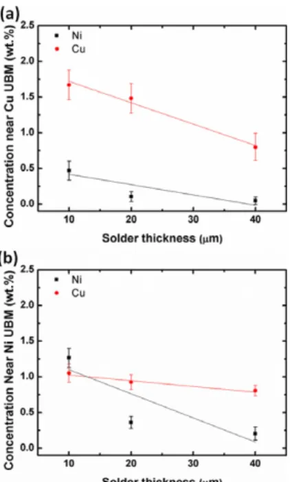
The measured Cu and Ni concentrations in the solder increase further as the solder thickness decreases to 10 lm. The measured Ni concentration is 1.27 ± 0.14, 0.673 ± 0.06 and 0.47 ± 0.13 wt.% at the three positions, respectively, whereas the Cu concentration increases to 1.05 ± 0.13, 1.20 ± 0.16 and 1.67 ± 0.21 wt.% at the three positions, respectively. The average Cu and Ni concentrations in this sample are 1.30 and 0.80 wt.%, respectively. Note that the values in the thin solder sam-ples are higher than those of the thicker solder samsam-ples. The results also clearly indicate that there exists an Ni concentration gradient inside the solder, decreasing from the Ni side to the Cu side.
Figure 4(a) and (b) shows plots of the measured Cu and Ni concentration in the solder at locations, respec-tively, closer to the IMC near the Cu UBM and the Ni UBM as a function of solder thickness. By compar-ingFigure 4(a) and (b), we can see clearly a concentra-tion gradient of Ni in the samples, especially in the 10 lm thick solder samples, which decreases from 1.27 wt.% near the Ni side to 0.47 wt.% near the Cu side. There could also be a concentration gradient of Cu in the sample, but, if so, it is much smaller. This is because of the formation of (Cu, Ni)6Sn5on both the Cu and Ni UBMs. Since the IMC is an equilibrium compound with Cu, the Cu solubility near the IMC should be the same. Thus we expect a small or no concentration gradient of Cu in the solder. On the other hand, the ratio of Cu and Ni in the IMC may differ slightly between the IMC on the Cu side and that on the Ni side. This effect may influ-ence the solubility slightly, but the effect on the Cu con-centration gradient will be small.
Chen et al.[13]reported that the Cu concentration in the solder has a significant effect on the interfacial IMC formation between the Sn–Cu solder and the Ni UBM.
Figure 3. The measured (Cu,Ni)6Sn5IMC (a) on the Cu side and (b)
on the Ni side for the three sets of samples.
When the Cu concentration in the Sn–Cu solder in-creases to 0.6 wt.%, the stable ternary IMC changes from (Ni, Cu)3Sn4to (Cu, Ni)6Sn5, the latter being more stable than the former. In the present study, most of the measured Cu concentrations in the solder are higher than 0.6 wt.% in all three sets of samples. Thus, the sta-ble IMC is (Cu, Ni)6Sn5on both the Cu and Ni sides. On the Ni side, no obvious layer of (Ni, Cu)3Sn4could be observed. Note that the measured Cu concentration at the Cu end in the10 lm thick sample is higher than the saturation solubility of Cu in SnAgCu solder at 260°C, which is 1.54 wt.% [14]. The Cu concentration at this location is larger than the saturation solubility. This is most likely due to the effect of the Gibbs–Thom-son potential, which increases the equilibrium concen-tration of solute around small precipitates, if we assume that there are many small ternary compound particles near the Cu UBM due to spalling or precipita-tion. On the other hand, the Ni saturation solubility in eutectic SnAg solders is 0.28 wt.% at 250°C [6]. Most of the measured Ni concentrations are also larger than the solubility limit, suggesting that many Ni atoms have precipitated out as tiny Cu–Ni–Sn IMC in the solder.
The dissolved Ni atoms may affect the Cu saturation solubility in the solder on the Ni side. Wang and Liu[9]
studied the interfacial reaction of Cu/150 lm Sn/Ni samples. They found that the IMC on the Ni side grew thicker than on the Cu side. They proposed that the sat-uration solubility of Cu may decrease from 1.1 to 0.6 wt.% when Ni atoms are present in the solder, result-ing in a Cu concentration gradient across the Sn layer.
When the thickness of the solder is reduced, the trend of ternary IMC formation is reversed. We propose a mechanism for this as follows. When the thickness of solder is reduced to 10 lm in a microbump, the forma-tion of IMC is different from that in flip-chip solder joints. The major influence comes from the effect of sol-der thickness on the solubility and concentration gradi-ent of Cu and Ni in the solder. The reduced thickness tends to increase the solubility and leads to the forma-tion of (Cu, Ni)6Sn5 on both sides of the solder joint. As we have mentioned above, since the IMC is an equi-librium compound with Cu, it will greatly reduce the concentration gradient of Cu across the solder joint, but not the Ni concentration gradient. The latter is the driving force of diffusion of Ni to the Cu side. It is nat-ural to expect a faster growth of the IMC on the Cu side, provided the supply of Ni is unrestricted.
In summary, the interfacial reactions in the liquid state have been studied in Ni/solder/Cu microbumps with 10, 20 and 40 lm thick SnAg solders. The IMC growth rate depends significantly on the thickness of the solder. The IMC thickness on the Cu side increases with decreasing solder thickness with a fixed reflow time. However, the IMC thickness on the Ni side decreases as the solder thickness is reduced for a fixed reflow time. Compositional analysis by EPMA indicates that the Cu and Ni concentrations in the solder increase with decreasing solder thickness. Furthermore, there is a con-centration gradient of Ni, but not Cu, across the micro-bumps, especially in the 10 lm thick solder samples. We propose that this is the mechanism that enhances the growth of the ternary IMC on the Cu side.
The financial support from the National Science Council, Taiwan, under contract NSC 98-2221-E-009-036-MY3, is acknowledged.
[1] J.C. Lin, W.C. Chiou, K.F. Yang, H.B. Chang, Y.C. Lin, E.B. Liao, J.P. Hung, Y.L. Lin, P.H. Tsai, Y.C. Shih, T.J. Wu, W.J. Wu, F.W. Tsai, Y.H. Huang, T.Y. Wang, C.L. Yu, C.H. Chang, M.F. Chen, S.Y. Hou, C.H. Tung, S.O. Jeng, D.C.H. Yu, IEDM, IEEE International (2010) 2.1.1–2.1.4.
[2] K.N. Tu, Microelectron. Reliab. 51 (2011) 517. [3] H.F. Hsu, S.W. Chen, Acta Mater. 52 (2004) 2541. [4] J. Shen, Y.C. Chan, S.Y. Liu, Acta Mater. 57 (2009) 5196. [5] M.S. Park, R. Arroyave, Acta Mater. 58 (2010) 4900. [6] C.P. Huang, C. Chen, C.Y. Liu, S.S. Lin, K.H. Chen, J.
Mater. Res. 20 (10) (2005) 2772.
[7] M. Kerr, N. Chawla, Acta Mater. 52 (2004) 4527. [8] M.O. Alam, Y.C. Chan, J. Appl. Phys. 98 (2005) 123527. [9] S.J. Wang, C.Y. Liu, Scripta Mater. 55 (2006) 347. [10] H.W. Tseng, C.Y. Liu, Mater. Lett. 62 (2008) 3887. [11] T.L. Shao, T.S. Chen, Y.M. Huang, C. Chen, J. Mater.
Res. 19 (2004) 3654.
[12] J.F. Li, P.A. Agyakwa, C.M. Johnson, Acta Mater. 59 (2011) 1198.
[13] W.T. Chen, C.E. Ho, C.R. Kao, J. Mater. Res. 17 (2002) 263.
[14] K. Zeng, K.N. Tu, Mater. Sci. Eng. R 38 (2002) 55.
Figure 4. (a) The measured Cu and Ni concentrations in the solder close to the Cu UBM as a function of solder thickness. (b) The measured Cu and Ni concentration in the solder close to the Ni UBM as a function of solder thickness.