Effects of strained InGaN interlayer on contact resistance between p - Ga N and indium
tin oxide
Chi-Ling Lee and Wei-I Lee
Citation: Applied Physics Letters 90, 181125 (2007); doi: 10.1063/1.2737122
View online: http://dx.doi.org/10.1063/1.2737122
View Table of Contents: http://scitation.aip.org/content/aip/journal/apl/90/18?ver=pdfcov Published by the AIP Publishing
Articles you may be interested in
Low-resistance, highly transparent, and thermally stable Ti/ITO Ohmic contacts to n - Ga N J. Vac. Sci. Technol. B 27, 1161 (2009); 10.1116/1.3136922
Investigation of Cr- and Al-based metals for the reflector and Ohmic contact on n - Ga N in GaN flip-chip light-emitting diodes
Appl. Phys. Lett. 89, 191122 (2006); 10.1063/1.2387888
Improvement of electrical and optical properties of p - Ga N Ohmic metals under ultraviolet light irradiation annealing processes
J. Vac. Sci. Technol. A 24, 634 (2006); 10.1116/1.2183192
Thermal stability improvement by using Pd NiO Al Ti Au reflective ohmic contacts to p -GaN for flip-chip ultraviolet light-emitting diodes
Appl. Phys. Lett. 88, 062113 (2006); 10.1063/1.2173245
Highly transparent and low resistance gallium-doped indium oxide contact to p -type GaN Appl. Phys. Lett. 87, 042109 (2005); 10.1063/1.1999012
This article is copyrighted as indicated in the article. Reuse of AIP content is subject to the terms at: http://scitation.aip.org/termsconditions. Downloaded to IP: 140.113.38.11 On: Thu, 01 May 2014 00:30:57
Effects of strained InGaN interlayer on contact resistance between p-GaN
and indium tin oxide
Chi-Ling Leea兲and Wei-I Lee
Department of Electrophysics, National Chiao Tung University, Hsinchu, 30010 Taiwan, Republic of China
共Received 6 December 2006; accepted 11 April 2007; published online 4 May 2007兲
Indium tin oxide 共ITO兲, with its transparency and strong adhesion to GaN, has been used as a replacement for Ni/ Au as a contact on p-GaN. However, ITO suffers from high contact resistance on p-GaN. In this work, low contact resistance between ITO and the p-GaN layer was consistently achieved using various strained InGaN layers as the interface layers between ITO and p-GaN layer. The doping of InGaN, whether n type or p type, has a relatively weak effect on the contact resistance as long as the thickness of the InGaN layer is adequately controlled. The secondary-ion-mass spectroscopy depth profile reveals that the n-type InGaN strained contact layer was also heavily doped with Mg. Results of this study demonstrate that the piezoelectric field between InGaN and p-GaN is important in reducing the barrier height of Ohmic contact. © 2007
American Institute of Physics. 关DOI:10.1063/1.2737122兴
GaN-based semiconductors are of great importance in fabricating visible and ultraviolet light-emitting diodes 共LEDs兲.1
In order to improve the light output power of LEDs, the contact resistance must be reduced and the trans-mission efficiency of the p-contact metal layer increased to achieve high-performance nitride-based LEDs. However, ob-taining Ohmic contacts on p-GaN is difficult because of the wide band gap and the high work function of p-GaN and because of the absence of metals having a work function that exceeds that of p-GaN. Most conventional nitride-based LEDs use semitransparent Ni/ Au on Mg-doped GaN as the
p-contact material. However, the transmittance of such a
semitransparent Ni/ Au共5 nm/8 nm兲 contact is only around 60%-75%. This problem can be solved using transparent in-dium tin oxide共ITO兲, instead of Ni/Au, as the contact ma-terial. ITO is a hard and chemically inert transparent material with high electrical conductivity and low optical absorption coefficient. The adhesion between ITO and GaN is also strong. These characteristics make ITO an attractive material for fabricating GaN-based LEDs. However, a good Ohmic contact has also been demonstrated to be difficult to achieve when ITO is deposited on p-GaN.2–5
In this work, LEDs with InGaN strained contact layers 共SCLs兲 of variously doped InGaN strained contact layers on the LEDs with ITO as transparency contact layer共TCL兲 were compared, and various thicknesses between the p-GaN layer and the ITO layer were also compared.
All of the samples used in this work are grown on 共0001兲-oriented sapphire using a low-pressure metal organic chemical vapor deposition reactor. The gallium, aluminum, indium, and nitrogen sources are trimethylgallium, trimethy-aluminum, trimethylindium, and ammonia 共NH3兲,
respec-tively. Bicyclopentadienylmagnesium 共Cp2Mg兲 and silane
共SiH4兲 are the p-type and n-type dopants, respectively. The
epilayer structures of all samples comprise a 25-nm-thick low-temperature GaN buffer layer grown at 550 ° C, fol-lowed by a 1.5-m-thick undoped u-GaN layer grown at 1050 ° C, a 1.5-m-thick highly conductive n-type GaN:Si layer grown at 1050 ° C, a five-period InGaN / GaN
multiple-quantum-well 共MQW兲 region grown at 760 °C, a 0.2-m-thick p-type AlGaN:Mg grown at 950 ° C, a 0.5-m-thick p-type GaN:Mg layer at 950 ° C, and 50-Å-thick heavy GaN:Mg-doped layer. Finally, various strained contact layers serve as an Ohmic contact layer. Two experiments, using different dopants and strained contact layers of different thicknesses, were performed to understand how the SCL affects the Ohmic contact between p-GaN and the ITO as TCL. In experiment A, 20-Å-thick undoped In-GaN, p+-InGaN and n+-InGaN were used as the SCLs. In experiment B, 0-, 20-, 40- and 60-Å-thick n+-InGaN layers
were used as the strained contact layer. The as-grown samples were then furnace annealed at 750 ° C in N2ambient to activate the Mg dopant.
In the device process procedure, wafers were partially etched until the n-GaN layer was exposed. Then, the 2000-Å-thick ITO TCL was evaporated onto the SCL to serve as a p-electrode. Finally, Cr/ Pt/ Au 共20 nm/50 nm/2m兲 metals were deposited on the
p-electrodes and the n-electrodes as bonding pads. The
pro-cessed wafer was then ground and polished down to 90m for chipping. The dimensions of the LED dies used in this study are 300⫻360m2.
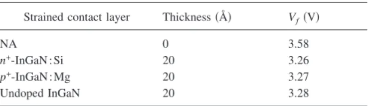
First, the LEDs with various dopant SCLs were fabri-cated to investigate the role of the InGaN SCLs with differ-ent dopants. As shown in Table I, LEDs with a 20-Å-thick undoped, heavily Si-doped, and heavily Mg-doped InGaN strained contact layer were compared with those without the SCL. The forward voltages of the LEDs with undoped, heavily Si-doped, and heavily Mg-doped InGaN strained contact layers are 3.28, 3.26, and 3.27 V, respectively, at a
a兲Electronic mail: [email protected]
TABLE I. Forward voltage of LED at driving current of 20 mA using strained InGaN contact layer with various dopants.
Strained contact layer Thickness共Å兲 Vf共V兲
NA 0 3.58
n+-InGaN : Si 20 3.26
p+-InGaN : Mg 20 3.27
Undoped InGaN 20 3.28
APPLIED PHYSICS LETTERS 90, 181125共2007兲
0003-6951/2007/90共18兲/181125/3/$23.00 90, 181125-1 © 2007 American Institute of Physics
This article is copyrighted as indicated in the article. Reuse of AIP content is subject to the terms at: http://scitation.aip.org/termsconditions. Downloaded to IP: 140.113.38.11 On: Thu, 01 May 2014 00:30:57
driving current of 20 mA. But the forward voltage of LED without SCL was as high as 3.58 V at a driving current of 20 mA. Comparing the LEDs with and without InGaN SCL, the forward voltage is about 0.3 V lower. These results re-veal that if the SCL were added on the LED and the thick-ness is small enough that the strain cannot be relieved, re-gardless of the dopant type of the strained layer the forward voltage can be reduced. The forward voltage of LEDs did not vary with the types of dopant. We believe that the dopant type of the SCLs was less important than the thickness of SCLs.
In order to investigate the role of dopant in SCLs, a 0.1-m-thick low-temperature grown undoped GaN was placed on the heavily Si-doped SCL with a standard LED structure to verify the doping concentration of the thin SCL. The secondary-ion-mass spectroscopy 共SIMS兲 depth profile is shown in Fig. 1; the Si doping concentration was 6⫻1016cm−3 and the Mg doping concentration was
8⫻1019cm−3 in the SCL, indicating that in the SCL, the
doping concentration of Si was much lower than that of Mg, which diffused out of the heavily Mg-doped layer. The SIMS depth profile reveals that even the heavily Si-doped and un-doped InGaN SCL were p+-type InGaN, which were formed by the diffusion of Mg from a heavily Mg-doped layer. Pre-viously, Sheu et al.,6 Margalith et al.,2 and Lin et al.4 re-ported that the ITO layer exhibits good Ohmic contact with the n-type GaN but poor Ohmic contact with the p-type GaN. The results of the SIMS indicate that the mechanism of good Ohmic contact does not only involve the ITO film’s forming an Ohmic contact with the n-type InGaN film and tunneling to the p-type GaN film.
The thickness of the InGaN SCL varied among 0, 20, 40, and 60 Å. As presented in Fig. 2, the thickness was varied from 0 to 20 Å and the forward voltage of the LEDs at the driving current of 20 mA decreased from 3.58 to 3.26 V, which lowered the voltage to 0.32 V. As the thickness was varied from 20 through 40 to 60 Å, the forward voltage in-creased from 3.26 through 3.39 to 3.45 V, respectively. These results indicate that the InGaN SCL can significantly reduce the resistivity of the Ohmic contact. If the thickness of the InGaN SCL is increased, then the forward voltage of the LED at a driving current of 20 mA increases, since the strain in the InGaN layer is relaxed. However, since the band gap of InGaN is equal to or less than 2.67 eV, the InGaN layer absorbs the light emitted from InGaN / GaN MQW, and
the increase in the thickness of the InGaN layer reduces the luminance intensity.
Figure 3 is the band diagram of the ITO/ p-InGaN / p-GaN heterointerface near the surface of LEDs, where ⌬⌽, ⌬⌽
⬘
, and ⌬⌽⬙
are the image-force-induced 共IFI兲 lowering item without SCL, with SCL, and with strain relaxed SCL, respectively. The main mechanisms of the mediate metal-semiconductor Ohmic contact are ther-mionic emission electrons, therther-mionic field emission elec-trons, and tunneling elecelec-trons, as presented in Fig.3共a兲. The item of q⌽Bis the barrier height at the interface without IFIFIG. 1. 共Color online兲 Depth profile of SIMS of a 0.1-m-thick undoped GaN on the strained contact layer with standard LED structure.
FIG. 2. 共Color online兲 Forward voltage and electrical photoluminance in-tensity of LED at a driving current of 20 mA as a function of thickness of n+-InGaN.
FIG. 3. 共Color online兲 Band diagrams of p-InGaN/p-GaN heterointerface near the surface:共a兲 without InGaN strained contact layer, 共b兲 with strained InGaN contact layer, and共c兲 with relaxed InGaN contact layer.
181125-2 C.-L. Lee and W.-I Lee Appl. Phys. Lett. 90, 181125共2007兲
This article is copyrighted as indicated in the article. Reuse of AIP content is subject to the terms at: http://scitation.aip.org/termsconditions. Downloaded to IP: 140.113.38.11 On: Thu, 01 May 2014 00:30:57
lowering item, which is simply the difference between the metal work function and the electron affinity. Since the elec-tric field at the metal-semiconductor interface produces an image force that reduces the barrier height,⌬⌽, the IFI low-ering item, is given by
⌬⌽ =
冑
qE 4s, 共1兲
where E is the piezoelectric field at the metal-semiconductor interface and s is the semiconductor permittivity. Finally,
the barrier height with IFI lowering item q⌽Bn is given by
q⌽Bn= q⌽B−⌬⍀. If an InGaN/GaN heterostructure is
present close to the surface, large band bending occurs be-cause of both the large piezoelectric polarization field and the electric field associated with the ionized acceptors at the surface depletion layer. Because a large piezoelectric polar-ization field formed at the InGaN / GaN layer, the IFI lower-ing factor, ⌬⌽
⬘
, becomes large, hence lowering the metal-semiconductor barrier, q⌽Bn, below that without the SCL. Inthe article of Takeuchi et al.,7theoretical results showed that the induced piezoelectric field in a strained Ga0.87In0.13N
layer is expected to be 1.1 MV/ cm. From Eq.共1兲, we can estimate the IFI lowering item to be about 0.35 eV; this value agrees with the results in Fig.2. When the SCL be-comes thicker, the piezoelectric field E will decrease due to strain relaxation and the IFI lowering item will become smaller. The heavily doped InGaN near 1019 cm−3 also
re-duces the surface depletion layer. Therefore, the tunneling barrier becomes thinner as shown in Fig.3共b兲, dramatically reducing the contact resistance.8
If the thickness of the InGaN contact layer exceeds the critical thickness, then the strain-induced piezoelectric field disappears because of the lattice relaxation, reducing the IFI lowering factor,⌬⌽
⬙
, and causing the barrier height of the metal-semiconductor to exceed that of the thinner InGaN SCLs. Thickening the InGaN SCL also reduces the tunnelingcurrent by increasing the tunneling barrier. Additionally, the potential spike at the InGaN / GaN heterointerface disturbs the transportation of holes, as presented in Fig.3共c兲. There-fore, the contact resistance increases with the SCL thickness, because the strain gradually relaxes as the thickness in-creases.
This study investigated the InGaN SCLs with various dopants and thicknesses. Experimental results indicate that even when various dopants are used in the strained InGaN films to form the contact layer, the Mg doping level is ex-tremely high, even in the heavily Si-doped InGaN SCLs. Additionally, the thickness of the InGaN SCLs is more im-portant than the dopant in the InGaN SCLs. We believe that the piezoelectric field between the strained InGaN layer and the p-GaN layer, which lowers the energy barrier at the sur-face, is important.
The authors are grateful for the financial support of this research by the National Science Council of Taiwan, Repub-lic of China, under Contract No. NSC 95-2112-M-009-001, and the Ministry of Education of Taiwan, Republic of China, under the MOE-ATU program.
1S. Nakamura, T. Mukai, and M. Senoh, Appl. Phys. Lett. 64, 1687共1994兲. 2T. Margalith, O. Buchinsky, D. A. Cohen, A. C. Abare, M. Hansen, S. P.
DenBaars, and L. A. Coldren, Appl. Phys. Lett. 74, 3930共1999兲. 3R. H. Horng, D. S. Wuu, Y. C. Lien, and W. H. Lan, Appl. Phys. Lett. 79,
2925共2001兲.
4Y. C. Lin, S. J. Chang, Y. K. Su, T. K. Tsai, C. S. Chang, S. C. Shei, C. W. Kuo, and S. C. Chen, Solid-State Electron. 47, 849共2003兲.
5K. M. Chang, J. Y. Chu, C. C. Cheng, and C. F. Chu, Phys. Status Solidi A 2, 2920共2005兲.
6J. K. Sheu, Y. K. Su, G. C. Chi, M. J. Jou, C. C. Liu, and C. M. Chang, Solid-State Electron. 43, 2081共1999兲.
7T. Takeuchi, S. Sota, M. Katsuragawa, M. Komori, H. Takeuchi, H. Amano, and I. Akasaki, Jpn. J. Appl. Phys., Part 2 36, L382共1997兲. 8K. Kumakura, T. Makimoto, and N. Kobayashi, Jpn. J. Appl. Phys., Part 1
42, 2254共2003兲.
181125-3 C.-L. Lee and W.-I Lee Appl. Phys. Lett. 90, 181125共2007兲
This article is copyrighted as indicated in the article. Reuse of AIP content is subject to the terms at: http://scitation.aip.org/termsconditions. Downloaded to IP: 140.113.38.11 On: Thu, 01 May 2014 00:30:57