and Ching-Te Chuang, Fellow, IEEE
Abstract—In this work, we propose a mixed TFET-MOSFET
8T SRAM cell comprising MOSFET cross-coupled inverters, dedicated TFET read stack and TFET write access transistors for ultra-low voltage operation. Exploiting both the merits of TFET and MOSFET devices, the proposed SRAM cell provides signif-icant improvement in SRAM stability, and performance. The stability and performance of the proposed cell are evaluated and compared with the conventional MOSFET 8T cell and pure TFET 8T cell using mixed-mode TCAD simulations based on published design rules for 22 nm technology node. Besides, the impacts of the device design of the proposed SRAM cell on the stability are also investigated. Various write-assist techniques to enhance the write-ability across 0.2 to 0.7 V for these SRAM cells are comparatively assessed. The results indicate that the proposed mixed TFET-MOSFET cell topology is viable for ultra-low voltage operation while MOSFET cell provides better stability and performance for high voltage operation.
Index Terms—Tunnel field-effect transistor (TFET), TFET
SRAMs, ultra-low voltage, write-assist circuits.
I. INTRODUCTION
R
EDUCING the power consumption in processors, mo-bile devices, and bio-medical electronics is one of the most challenging task. Voltage scaling is an efficient way to reduce the power consumption. The conventional 6T SRAM cell achieves large storage capacity. However, it suffers from read disturb, half-select disturb, and the conflicting read/write requirements. Consequently, the stability of 6T SRAM cell de-grades significantly as scales down, limiting the achiev-able for overall system.Tunnel field-effect transistor (TFET) device with the band-to-band tunneling as the major current transport mechanism en-ables steeper than 60 mV/dec subthreshold swing, and is con-Manuscript received March 28, 2014; revised July 16, 2014; accepted September 16, 2014. Date of publication October 22, 2014; date of cur-rent version December 09, 2014. This work was supported in part by the Ministry of Science and Technology in Taiwan under Contract MOST 103-2221-E-009-196-MY2 and MOST 103-2917-I-009-181. This paper was recommended by Guest Editor S. Mukhopadhyay.
The authors are with the Department of Electronics Engineering and the In-stitute of Electronics, National Chiao Tung University, Hisnchu, 30010 Taiwan (e-mail: [email protected]; [email protected]).
Color versions of one or more of the figures in this paper are available online at http://ieeexplore.ieee.org.
Digital Object Identifier 10.1109/JETCAS.2014.2361072
sidered as a promising device to replace MOSFET device for ultra-low voltage/power operation [1]–[5]. However, the asym-metric source/drain design and transport mechanism result in uni-directional current conduction [6], which severely impacts the pass-gate based circuits and SRAMs [6]–[9].
In this work, we propose a mixed TFET-MOSFET 8T SRAM cell which exploits both the advantages of TFET and MOSFET devices for ultra-low voltage operation. The merits of the pro-posed cell versus the conventional MOSFET 8T SRAM cell and the pure TFET 8T SRAM cell in stability and performance are comprehensively assessed [26]. Besides, the impacts of the threshold voltage design of the MOSFET and TFET devices and the device design parameters of the TFET devices on the SRAM stability and are also investigated. With increasing vari-ability for scaled devices, read/write-assist circuits are indis-pensable for SRAM, especially at low voltage. Various assist techniques including the negative bit-line (NBL) write-assist [22], transient voltage collapse (TVC) write-write-assist [23], [24], and data-aware write-assist [25] are extensively assessed and compared for these SRAM cells.
This paper is organized as follows. Section II introduces the device design, characteristics, and TCAD simulation method-ology used in this work. Section III describes the proposed mixed TFET-MOSFET 8T cell including the impacts of dif-ferent device designs. Section IV presents the cell layouts based on published design rules for 22 nm technology node. Sec-tion V comparatively addresses the stability and performance, and evaluates various write-assist circuit techniques for these SRAM cells. Section VI concludes the paper.
II. DEVICEDESIGN, TCAD METHODOLOGY,AND SWITCHINGCHARACTERISTICS
A. Device Design and TCAD Methodology
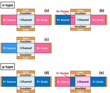
In this work, we consider the PNPN type TFET [3] for its capability to achieve sub-threshold swing below 60 mV/dec at room temperature. The device structures of the PNPN TFET, p-i-n TFET and conventional MOSFET are shown in Fig. 1. Notice that p-i-n TFET, with inferior sub-threshold swing and drive current compared with PNPN TFET [27], is included here for investigation of the stability and of the proposed mixed SRAM cell with different TFET device designs hence different TFET device characteristics in Section IV. Double-gate (DG) 2156-3357 © 2014 IEEE. Personal use is permitted, but republication/redistribution requires IEEE permission.
Fig. 1. Structures of (a) n-type MOSFET, (b) n-type PNPN TFET, (c) n-type p-i-n TFET, (d) p-type MOSFET, and (e) p-type NPNP TFET.
structures are used, with the gate length 25 nm, sil-icon body thickness 6 nm, equivalent oxide thickness
0.6 nm, high- dielectric
, the and regions doped to /cm , and the
pocket region doped to /cm . Fig. 2 shows the Ids-Vgs characteristics of the TFET (PNPN/NPNP), p-i-n TFET, and
and DG MOSFET (N/PMOS) at V. The
TFET and MOSFET devices/circuits are analyzed using atom-istic TCAD mixed-mode simulations. The nonlocal band-to-band tunneling model which is applicable to arbitrary tunneling barrier with nonuniform electric field is used for TFET simula-tions [16]. The tunneling paths are dynamically determined ac-cording to the gradient of the band energy. The ratio and S.S. of PNPN TFET device are calibrated with [3] and the OFF state current is set with available Si TFET experimental data. The p-i-n TFET device is designed to have the same OFF state current as the PNPN TFET device. The DG MOSFET devices with two different designs are considered to investigate the impact of different MOSFET designs on the SRAM stability and performance. The MOSFET device is designed with the same OFF state current as the PNPN TFET device for low power operation, while the MOSFET device is designed with higher leakage current around pA/ m as shown in Fig. 2. The PNPN TFET device can be seen to have superior current drive and subthreshold slope at very low gate bias, followed by a broad soft transition region before its current saturates. While at high gate bias, the current drive of PNPN TFET device is in-ferior to the MOSFET.
B. Device and Circuit Switching/Output Characteristics
Fig. 3 show the switching Id-Vds characteristics of MOSFET and PNPN TFET devices in an in-verter. The delayed saturation in TFET device results in large cross-over region/current between the n-type and p-type de-vices in TFET inverter which degrades the sharpness of voltage transfer characteristic (VTC) of the TFET inverter and the
Fig. 2. Ids-Vgs characteristics at V of n-/p-type DG and MOSFET devices, DG PNPN/NPNP TFET devices, and DG p-i-n TFET device.
Fig. 3. Device switching characteristics of (a) DG MOSFET, (b) DG MOSFET, and (c) DG TFET in an inverter.
stability in TFET SRAM cell. In the following sections, “p-i-n TFET” will be explicitly stated, and “TFET” will be used for “PNPN” TFET devices for simplicity.
III. ULTRA-LOWVOLTAGESRAM CELLDESIGNS
A. Conventional MOSFET/TFET 8T SRAM Cell
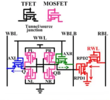
The conventional 6T SRAM cell faces many challenges with increasing variations in deep sub-100 nm technologies [10], es-pecially at low supply voltages. Alternative SRAM cells such as 8T cell and 10T cell have been proposed for robust low voltage operations [11]–[15]. In this work, the conventional 8T SRAM cell [11], which utilizes dedicated read buffer to decouple the read current from the cell storage node to eliminate the read disturb and enhance the read stability, is used as the basic cell structure due to its technical viability with uni-directional TFET devices. Fig. 4 shows the schematics of MOSFET/TFET 8T SRAM cell structures and the corresponding read/write current paths. The bracket in the symbol of TFET device indicates the tunnel junction in the TFET device.
For MOSFET 8T SRAM cell, the read disturb is eliminated through the dedicated read stack which decouples the cell storage nodes from read current while the bi-directional write access transistors provide the “push-pull” action to enhance write-ability during write operation. However, MOSFET 8T SRAM cell suffers from write half-select disturb (Fig. 5) where the half-select cells on the selected row
perform “dummy” read, thus experiencing cell disturb similar to the read disturb in the conventional 6T cell. The MOSFET 8T SRAM cell is thus not suitable for bit-interleaving architecture.
Fig. 4. Cell structures and corresponding read/write paths for (a) conventional MOSFET 8T SRAM cell and (b) TFET 8T SRAM cell.
Fig. 5. Schematic of 8T SRAM cell array showing the selected cell for Write and half-select disturb current path through the half-selected cell for MOSFET 8T SRAM.
For TFET 8T SRAM cell, the read stability is improved by the dedicated read stack as in the MOSFET 8T cell. Moreover, the superior current drive and subthreshold slope of TFET at low voltage significantly enhance the read performance over the MOSFET 8T cell at low voltage. Furthermore, the uni-directional write access transistors eliminate write half-se-lect disturb, thus facilitating bit-interleaving architecture for enhanced soft error immunity with error correction code (ECC) [17]. However, there are two drawbacks for the TFET 8T cell. First, the large cross-over region in TFET device degrades the hold/read static noise margin (HSNM/RSNM) and write static noise margin (WSNM). Secondly, the lack of “push-pull” action during write operation due to uni-directional write access transistors degrades the write-ability.
B. Mixed TFET-MOSFET 8T SRAM Cell
Based on the previous discussion of the pros and cons of MOSFET and TFET 8T SRAM cells and realizing that mixing TFET and MOSFET devices is manufacturally possible since the process of TFET device is compatible with CMOS process [5], Fig. 6 shows the proposed mixed TFET-MOSFET 8T SRAM cell and corresponding read/write paths. The cell fea-tures MOSFET cross-coupled inverters for improved HSNM and RSNM, dedicated TFET read stack for enhanced read
Fig. 6. Cell structure and corresponding read/write paths of proposed mixed TFET-MOSFET 8T SRAM cell where MOSFET devices are used in the cross-coupled inverter pair.
stability and read performance and TFET write access tran-sistors to facilitate bit-interleaving architecture. Furthermore, with MOSFET cross-coupled inverters, the write-ability of the proposed mixed TFET-MOSFET 8T cell is significantly enhanced over the MOSFET 8T cell and TFET 8T cell in the low voltage regime due to the disparity of the current drive between the write access TFET device and the holding (pull-up) PMOSFET at low voltage. By properly designing the TFET and MOSFET devices to increase the voltage where TFET current and MOSFET current cross-over (e.g., III-V TFET or designs on MOSFET and TFET devices), the effective voltage range for improved write-ability of the mixed TFET-MOSFET cell will be broadened. The impact of different TFET device design (e.g., p-i-n TFET) and the design of the MOSFET device on the SRAM stability and performance of the mixed TFET-MOSFET 8T cell will be addressed in Section IV. Exploiting both the merits of TFET and MOSFET devices, the proposed mixed TFET-MOSFET 8T cell provides significant improvement in SRAM stability, and perfor-mance for ultra-low voltage operation. It should be noted that the proposed cell utilizes the disparity of current drive between TFET device and MOSFET device for improved write-ability at ultra-low voltage. However, at higher supply voltage, the current drive disparity reverses, and MOSFET device provides higher current drive than the TFET device (Fig. 2). While TFET-based circuits aim at energy-efficient ultra-low voltage operation, it would be desirable in practice to cover higher range up to 0.5–0.7 V. Hence, write-assist circuits to extend TFET or mixed TFET-MOSFET SRAM cell operation to 0.5–0.7 V need to be developed. This will be addressed in Section V.
IV. STABILITY ANDLAYOUT
In this section, the stability and layout of the MOSFET, TFET, and mixed TFET-MOSFET 8T SRAM cell are comparatively assessed.
A. Stability
Fig. 7 show the respective hold, read, write, and half-select SNM of the and H MOSFET 8T cell, TFET 8T cell, mixed p-i-n TFET-MOSFET 8T cell comprising MOSFET cross-coupled inverters and mixed TFET-MOSFET
Fig. 7. Stability of and MOSFET 8T SRAM cell, TFET SRAM cell, mixed p-i-n TFET-MOSFET 8T SRAM cell comprising MOSFET cross-coupled inverter and mixed TFET-MOSFET 8T SRAM cell comprising and MOSFET cross-coupled inverter across V–0.7 V: (a) HSNM, (b) RSNM, (c) WSNM, and (d) HSSNM.
Fig. 8. Butterfly curves of TFET and mixed TFET-MOSFET 8T SRAM cell comprising MOSFET cross-coupled inverter in hold/read modes at
0.4 V and 0.2 V.
8T cell comprising and MOSFET cross-coupled
inverters, respectively, for ranging from 0.2 V to 0.7 V. 1) Hold/Read SNM
For 8T cell configuration, the read SNM (RSNM) equals hold SNM (HSNM). As shown in Fig. 7(a) and (b), both
the and MOSFET 8T cell and the mixed
TFET-MOSFET 8T cell comprising of and MOSFET cross-coupled inverters exhibit comparable HSNM and RSNM. The TFET 8T cell shows larger degradation in both HSNM and RSNM, especially for V, due to the large cross-over region in TFET devices which degrades the sharpness of cell inverter VTC and can be observed in the transition region of the butterfly curves shown in Fig. 8. The actual amount of degradation will depend on the output conductance of the manufactured TFET devices and MOSFET devices
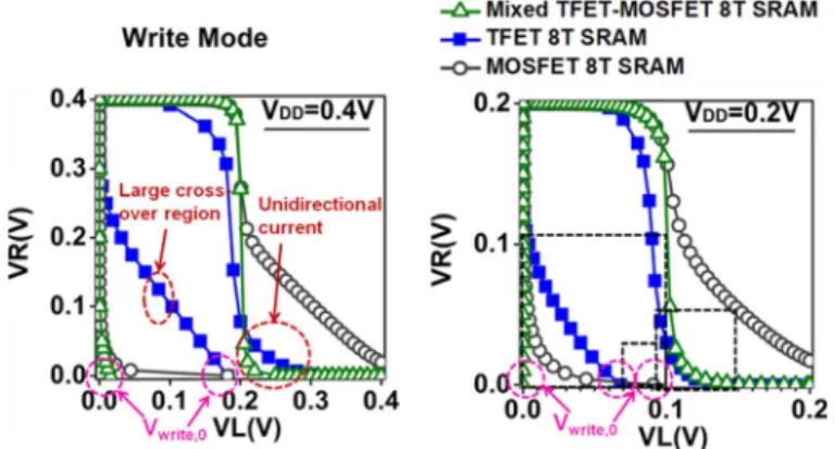
Fig. 9. Butterfly curves of MOSFET, TFET, and mixed TFET-MOSFET 8T SRAM cell comprising MOSFET cross-coupled inverters in write mode at 0.4 V and 0.2 V.
in weak inversion conditions. As scales down to 0.2 V, the HSNM/RSNM degradation of the TFET 8T cell becomes less as cross-over region in TFET devices is reduced.
2) Write SNM
Fig. 7(c) shows the write SNM (WSNM) of the SRAM cell topologies versus . The TFET 8T cell shows significant degradation in WSNM across range from 0.2 V to 0.7 V since the uni-directional conduction of TFET write-access transistor deprives the push-pull action during write operation, which can be observed in the write butterfly curves of TFET and mixed TFET-MOSFET 8T cell in Fig. 9(a). Meanwhile, the large cross-over region in TFET devices causes large (determined by the current balance between the write access transistor and the holding transistor) as shown in Fig. 9(a), thus further degrading the write-ability. As scales down to 0.2 V, the WSNM of TFET 8T cell becomes comparable to that of MOSFET 8T cell as shown in Fig. 9(b) since the cross-over transition region is reduced. Among the SRAM cell topologies, for low voltage operation ( V), the proposed mixed TFET-MOSFET 8T cell comprising MOSFET cross-coupled inverter exhibits superior WSNM with 150% to 310% improvement compared with the TFET 8T SRAM cell. While the proposed cell still lacks push–pull action during write operation, the is significantly reduced, especially at low volt-ages, due to the steep swing of the TFET device and the disparity of current drive between the write access TFET and the holding PMOSFET, thus providing most significant improvement in write-ability among all these SRAM topologies. However, for the proposed mixed TFET-MOSFET 8T cell comprising MOSFET de-vices and that of the proposed mixed cell using p-i-n TFET and MOSFET devices, they exhibit worse write-ability and the WSNM diminishes at 0.5 V. This is due to decrease of the drive current disparity be-tween the write access PNPN TFET/p-i-n TFET devices
and holding PMOSFET. It should be noted
Fig. 10. Weighting of versus of MOSFET 8T SRAM cell, TFET 8T SRAM cell, mixed p-i-n TFET-MOSFET 8T SRAM cell comprising HVT MOSFET cross-coupled inverter, and mixed TFET-MOSFET 8T SRAM cell comprising and MOSFET cross-coupled inverter from 0.2 V to 0.7 V.
is suitable for other MOSFET and TFET device structures. However, since the ON state current of the TFET device and the subthreshold swing are not as good as PNPN TFET device, and the MOSFET device has very low threshold voltage, the write-ability becomes worse and the write operation range becomes narrower. Hence, the MOSFET and TFET device should be carefully designed to have large write operation range.
It should also be noticed that the WSNM of the mixed TFET-MOSFET 8T cell shows an unique reflective trend as indicated by the dashed lines in Fig. 7(c) and the margin vanishes as is raised above 0.6 V for mixed TFET-MOSFET SRAM cell comprising cross-cou-pled inverters, while the WSNMs of MOSFET and TFET 8T cells exhibit monotonic trend with . This is be-cause as becomes higher, the current drive of the holding PMOSFET overwhelms that of the write access TFET as shown in Fig. 2, resulting in significantly larger which can be observed in Fig. 10. As a result, write failure occurs. On the other hand, when scales down to below 0.6 V, the disparity of the current between the holding PMOSFET and write access TFET re-verses and write stability improves. Between 0.5 V and 0.4 V, the decrement of of the proposed cell is larger than the reduced margin caused by lowered supply voltage which can be clearly seen with the weighting of
versus shown in Fig. 10, thus causing a reflection point near 0.4 V. Similar trend can be observed for mixed TFET-MOSFET SRAM cell comprising cross-coupled inverters and for mixed cell using p-i-n TFET device and cross-coupled MOSFET devices. The proposed cell with MOSFET devices provides
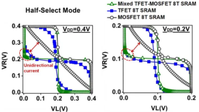
Fig. 11. Butterfly curves of MOSFET, TFET, and mixed TFET-MOSFET 8T SRAM cell comprising MOSFET cross-coupled inverters in half-selected mode at 0.4 V and 0.2 V.
sufficient write-ability at ultra-low supply voltage for below 0.5 V. Additional write-assist circuit would be required to extend above 0.6 V, and will be discussed in Section V.
3) Half-Select SNM
Fig. 7(d) shows the half-select SNM (HSSNM) of the SRAM cell topologies versus . It is observed that TFET, mixed TFET-MOSFET, and mixd p-i-n TFET-MOSFET 8T cells with uni-directional TFET write access transistors show larger HSSNM than the MOSFET 8T cell. At 0.5 V, the enhancement of HSSNM of mixed TFET-MOSFET 8T cell is about 106% and 50% compared with the MOSFET 8T cell and TFET 8T cell, respectively. The large improvement results from the fact that with uni-directional TFET write access transis-tors, the “dummy” read current of the half-selected cells cannot flow through the cell storage nodes, hence the half-selected disturb is significantly reduced. This can be clearly observed in the butterfly curves shown in Fig. 11 indicated by the spanning arrows. For the proposed mixed TFET-MOSFET 8T cell with the MOSFET cross-coupled inverters, the HSSNM improves further due to sharper VTC (reduction of the cross-over region) compared with the TFET cross-coupled inverters as shown in Fig. 11. The stabilities of the SRAM cell topologies are summa-rized in Table I where the indicates operating at
low supply voltages ( 0.5 V) and
indi-cates operating at high supply voltages. The circle symbol indicates excellent stability, the triangle indicates mod-erate stability, while the cross stands for poor stability. It is clear that for operating at ultra-low voltage, the pro-posed mixed TFET-MOSFET 8T SRAM cell comprising cross-coupled inverters provides substantial merits over the MOSFET and TFET 8T SRAM cell. While for operating at high supply voltage, the MOSFET 8T SRAM cell appears to provide better stability.
For the following section, we will assess the layout and SRAM performance. Here, we use the MOSFET, TFET, and mixed TFET-MOSFET 8T cell comprising MOSFET cross-coupled inverters as examples.
TABLE I
COMPARISON OFSTABILITY FOR MOSFET 8T SRAMCELL, TFET 8T SRAM CELL, MIXEDp-i-n TFET-MOSFET 8T SRAM CELLCOMPRISING
MOSFET CROSS-COUPLEDINVERTER ANDMIXEDTFET-MOSFET 8T SRAM CELLCOMPRISING AND MOSFET CROSS-COUPLED
INVERTER FOROPERATING ATLOWSUPPLYVOLTAGE ANDHIGHSUPPLY
VOLTAGE, RESPECTIVELY
B. Layout
Fig. 12(a), (b), and (c) shows the layout of MOSFET, TFET, and mixed TFET-MOSFET 8T cells, respectively. The layouts are based on published design rules for 22 nm technology node and proportionally estimated parameters [18]. Table II summa-rizes the pertinent design rules used in this work. Specifically, due to the asymmetrical source/drain design of TFET device, its source and drain are unexchangeable hence the layout of the TFET cell differs from that of the conventional MOSFET cell. As shown in Fig. 12(a) for MOSFET 8T cell, the source and drain of the stacked read transistors are exchangeable and can be shared. While in Fig. 12(b) and (c), for TFET and mixed TFET-MOSFET 8T cell, the stacked read transistors are TFET devices, and the vertical direction of the bit cells are expanded resulting from the unexchangeable source/drain, and the height of the bit cells is constrained by the minimum spacing rules be-tween the diffusion layers. The area overhead of the TFET and mixed TFET-MOSFET 8T cell is about 27% compared with the MOSFET 8T cell.
V. PERFORMANCE ANDWRITE-ASSISTCIRCUITTECHNIQUES The performance of SRAM arrays with 16 cells per bit-line are assessed considering the worst case bit-line data pattern and bit-line loading estimated from the layout. As shown in
Fig. 12. Layout of (a) MOSFET 8T SRAM cell, (b) TFET 8T SRAM cell, and (c) mixed TFET-MOSFET 8T SRAM cell based on design rules listed in Table II.
TABLE II LAYOUTDESIGNRULES
Fig. 13(a), TFET 8T cell and mixed TFET-MOSFET 8T cell significantly outperform the MOSFET 8T cell in “cell” read ac-cess time (defined as the time from when selected read word-line (RWL) reaches half- to when the read bit-line (RBL) is pulled down to half- for below 0.5 V, providing 4000x improvement at 0.2 V. On the other hand, for above 0.6 V, MOSFET 8T cell provides better “cell” read performance with 10x improvement at 0.7 V com-pared with TFET and mixed TFET-MOSFET 8T cell. This is
Fig. 13. Performance comparison of the MOSFET, TFET, and mixed TFET-MOSFET 8T SRAM cell for (a) cell read access time and (b) cell time-to-write.
because for below 0.5 V, TFET read transistors offer supe-rior current drive and steep subthreshold swing compared with MOSFET devices, while for above 0.6 V, the current dis-parity reverses. Fig. 13(b) shows the “cell” time-to-write (de-fined as the time from the 50% activation of the Write Word-Line (WWL) to the time when the voltage of the cell storage node (pulling to “1”) reaches 90% . For below 0.5 V, both MOSFET 8T cell and mixed TFET-MOSFET 8T cell ex-hibit substantial longer time-to-write than the TFET 8T cell. The “writing” process consists of two phases. In the initial phase of write operation, the write access transistor competes with the holding (pull-up) transistor to pull down the cell “1” storage node. In the second phase, the pull-up transistor of the oppo-site cell inverter pulls up the oppooppo-site cell “0” storage node to trigger the feedback/latching mechanism to complete the write operation. For mixed TFET-MOSFET 8T cell, the write access transistor pull down the cell “1” storage node quickly due to the superior current drive of TFET at low voltage. However, owing to lack of push-pull action and the low current drive of pull-up PMOSFET, the pull-up of the opposite cell “0” storage node (second phase of the write operation) is impeded, thus degrading
0.6 V, the current drive of the holding PMOSFET overwhelms that of the write access TFET in mixed TFET-MOSFET 8T cell, hence write failure occurs. For the proposed cell, write-assist circuit techniques would be necessary to extend the operation to higher voltage and will be discussed in Section V-B.
A. Low Voltage Operation
1) Negative Bit-Line Write-Assist: The cell time-to-write
at low supply voltage can be improved by write-assist circuit techniques such as: 1) collapsing cell [19], 2) raising cell [20], 3) boosting write WL [21], and 4) negative write bit-line voltage [22]. Among these write-assist techniques, collapsing cell and raising cell will result in degra-dation of stability of unselected cells on the selected column, while the boosting write WL will aggravate half-select disturb. In this work, we consider the NBL write-assist (Fig. 14) to improve the cell write performance of the MOSFET and mixed TFET-MOSFET 8T cell. The transient waveforms during write operation of the proposed mixed TFET-MOSFET 8T SRAM cell with and without NBL write-assist circuit are shown in Fig. 16. The comparison of the improvement in cell time-to-write between the proposed mixed TFET-MOSFET and MOSFET 8T cell with the NBL write-assist technique is shown in Fig. 15. The results indicate that the proposed mixed TFET-MOSFET 8T cell using NBL write-assist shows larger improvement compared with the MOSFET 8T cell with NBL write-assist for below 0.5 V. This is because TFET access transistor with increased overdrive voltage due to NBL exhibits larger drive current improvement in both the initial and second phase of write operation compared with the MOSFET access transistor. Moreover, with the uni-directional conduction of TFET driver transistor, the current charging up the bit-line would be smaller compared with the MOSFET driver transistor, thus facilitating the cell time-to-write further.
B. High Voltage Operation
It is pointed out that the proposed mixed TFET-MOSFET 8T SRAM cell faces write failure for above 0.6 V due to the reverse of current drive disparity between the TFET access tran-sistor and PMOSFET holding trantran-sistor. In this part, we con-sider write-assist circuit techniques including transient voltage collapse write-assist [23], [24] and the data-aware write-assist scheme [25] to enhance the write-ability of the proposed mixed TFET-MOSFET cell.
1) Transient Voltage Collapse Write-Assist: The schematic
of the transient voltage collapse write-assist circuit is shown in Fig. 17. Transient voltage collapse write-assist dynamically pulls down the selected column cell supply below the
Fig. 14. Schematic of NBL write-assist for (a) the proposed mixed TFET-MOSFET 8T SRAM cell and (b) pure TFET-MOSFET 8T SRAM cell.
data-retention voltage during write operation. The scheme offers fast cell supply collapse for effective write-assist. How-ever, the TVC pulse width must be carefully controlled to ensure data retention of unselected cells in the selected column. The simulated transient waveforms during write operation at 0.6 V are shown in Fig. 18. It is clearly seen that with the transient voltage collapse write-assist, the proposed mixed TFET-MOSFET 8T SRAM cell performs write successfully.
2) Data-Aware Write-Assist: The schematic of the data-aware write-assist circuit is shown in Fig. 19 where the virtual cell supply nodes and for the left-and right-half cells of a column are controlled by separate power-switch/keeper pairs. During write operation, the keepers
Fig. 15. Improvement in cell time-to-write of MOSFET and mixed TFET-MOSFET 8T cell with negative bit-line write-assist.
Fig. 16. Write transient waveforms of the proposed mixed TFET-MOSFET 8T SRAM cell with and without negative bit-line write-assist. Inset of the bottom figure shows the time when the write operation completes for the proposed mixed TFET-MOSFET 8T SRAM cell without negative bit-line write-assist.
are turned off, and the virtual cell supply node of the write “0” side (assuming becomes floating due to the low-going WBL. The virtual cell supply node goes low due to write current and leakage of cells in the column, thus reducing of the holding PMOSFET and contention with the write access transistor. The pertinent transient waveforms during write are shown in Fig. 20. Compared with the transient voltage collapse write-assist in Fig. 19, the data-aware write-assist offers more significant write-ability and write performance improvement for the proposed mixed TFET-MOSFET 8T SRAM. This is because in the data-aware write-assist, the strength of pull-up
Fig. 17. Schematic of TVC write-assist scheme for the proposed mixed TFET-MOSFET 8T SRAM.
Fig. 18. Write transient waveforms of the proposed mixed TFET-MOSFET 8T SRAM cell with and without TVC write-assist.
PMOSFET of the opposite half-cell and the latch feedback effect are not affected since for the opposite half cell remains at . On the other hand, in the transient voltage collapse write-assist, due to the lowering of the cell supply of the opposite half cell, the second phase of the write operation is retarded.
Fig. 19. Schematic of data-aware write-assist scheme for the proposed mixed TFET-MOSFET 8T SRAM.
Fig. 20. Write transient waveforms of the proposed mixed TFET-MOSFET 8T SRAM cell with and without data-aware write-assist.
The cell time-to-write of the proposed mixed TFET-MOSFET 8T SRAM cell with transient voltage collapse write-assist and the data-aware write-assist are shown in Fig. 13(b) indicated by solid triangular and star symbol. With data-aware write-assist, the proposed mixed TFET-MOSFET 8T SRAM cell offers 40% improvement in cell time-to-write
compared with that using the transient voltage collapse write-assist at high supply voltages.
VI. CONCLUSION
We propose a mixed TFET-MOSFET 8T SRAM cell com-prising MOSFET cross-coupled inverters, dedicated TFET read stack and TFET write access transistors suitable for ultra-low voltage operation. The use of MOSFET cross-coupled inverters improves hold static noise margin (SNM) over the pure TFET cell. The TFET read stack improves the “cell read access time” by 1.6x and 4000x at 0.5 V and 0.2 V, respectively, compared with the MOSFET 8T cell due to the superior current drive and subthreshold slope of TFET at low supply voltages. The uni-directional TFET write access transistors eliminate the write half-select disturb to facilitate bit-interleaving architecture for improved soft error immunity with ECC compared with MOSFET 8T cell. The disparity in current drive between TFET write access transistor and MOSFET holding (pull-up) transistor greatly improves WSNM for supply voltage below 0.5 V. The proposed cell improves the cell hold/read stability, write stability, read performance, and eliminate half-select disturb for ultra low voltage operations. The layout and performance of the MOSFET, TFET, and proposed mixed TFET-MOSFET 8T cell are com-paratively assessed. With negative bit-line write-assist, the cell time-to-write is significantly enhanced compared with the MOSFET 8T cell using NBL write-assist at low supply voltages. To operate at higher supply voltage for above 0.6 V, the proposed mixed TFET-MOSFET 8T cell adopting the transient voltage collapse write-assist or data-aware write-assist shows adequate write-ability. Among these SRAM cells, MOSFET 8T cell offers better cell stability and performance at higher supply voltage for above 0.6 V. With superior stability and read performance, the proposed mixed TFET-MOSFET cell provides merits for ultra-low voltage operation.
ACKNOWLEDGMENT
The authors would like to thank the National Center for High-Performance Computing in Taiwan for the software and facilities.
REFERENCES
[1] J. Appenzeller, Y.-M. Lin, J. Knoch, and Ph. Avouris, “Band-to-band tunneling in carbon nanotube field-effect transistors,” Phys. Rev. Lett., vol. 93, no. 19, pp. 196805 (1–3)–, Nov. 2004.
[2] S. H. Kim, H. Kam, C. Hu, and T.-J. K. Liu, “Germanium-source tunnel field effect transistors with record high ,” VLSI Tech., pp. 178–179, 2009.
[3] V. Nagavarapu, R. Jhaveri, and J. C. S. Woo, “The tunnel source (PNPN) n-MOSFET: A novel high performance transistor,” IEEE
Trans. Electron Devices, vol. 55, no. 4, pp. 1013–1019, Apr. 2008.
[4] A. C. Seabaugh and Q. Zhang, “Low-voltage tunnel transistors for be-yond CMOS logic,” Proc. IEEE, vol. 98, no. 12, pp. 2095–2110, Dec. 2010.
[5] F. Mayer, C. Le Royer, J.-F. Damlencourt, K. Romanjek, F. Andrieu, C. Tabone, B. Previtali, and S. Deleonibus, “Impact of SOI, Si1-xGexOI and GeOI substrates on CMOS compatible tunnel FET performance,” in IEDM. Tech. Dig., 2008, vol. 163.
[6] J. Singh, K. Ramakrishnan, S. Mookerjea, S. Datta, N. Vijaykrishnan, and D. Pradhan, “A novel Si-tunnel FET based SRAM design for ultra-low power 0.3 V VDD applications,” Proc. ASP-DAC, pp. 181–186, 2010.
[7] D. Kim, Y. Lee, J. Cai, I. Lauer, L. Chang, S. J. Koester, D. Sylvester, and D. Blaauw, “Low power circuit design based on heterojunction tunneling transistors (HETTs),” in Symp. Low Power Electron. Design, 2009, pp. 219–224.
[8] X. Yang and K. Mohanram, “Robust 6T Si tunneling transistor SRAM design,” in Proc. Design Automat. Test Eur., 2011, pp. 1–6. [9] V. Saripalli, S. Datta, V. Narayanan, and J. P. Kulkarni,
“Variation-tolerant ultra low-power heterojunction tunnel FET SRAM design,” in
Symp. Nanoscale Archit., 2011, pp. 45–52.
[10] C.-T. Chuang, S. Mukhopadhyay, J. J. Kim, K. Kim, and R. Rao, “High performance SRAM in nanoscale CMOS: Design challenges and tech-niques,” in IEEE Int. Workshop Memory Technol., Design Test., Dec. 3–5, 2007, pp. 4–12.
[11] L. Chang, D. M. Fried, J. Hergenrother, J. W. Sleight, R. H. Dennard, R. K. Montoye, L. Sekaric, S. J. McNab, A. W. Topol, C. D. Adams, K. W. Guarini, and W. Haensch, “Stable SRAM cell design for the 32 nm node and beyond,” in Symp. VLSI Technol. Dig., Jun. 14–16, 2005, pp. 128–129.
[12] R. Joshi, R. Houle, K. Batson, D. Rodko, P. Patel, W. Houtt, R. Franch, Y. Chan, D. Plass, S. Wilson, and P. Wang, “6.6_ GHz low vmin, read and half select disturb-free 1.2 Mb SRAM,” in IEEE Symp. VLSI
Cir-cuits Dig., Jun. 14–16, 2007, pp. 250–251.
[13] M.-H. Chang, Y.-T. Chiu, S.-L. Lai, and W. Hwang, “A 1 kb 9T sub-threshold SRAM with bit-interleaving scheme in 65 nm CMOS,” in
Proc. Int. Symp. Low Power Electron. Design, Aug. 1–3, 2011, pp.
291–296.
[14] I. J. Chang, J. J. Kim, S. P. Park, and K. Roy, “A 32 kb 10T sub-threshold SRAM array with bit-interleaving and differential read scheme in 90 nm CMOS,” IEEE J. Solid-State Circuits, vol. 44, no. 2, pp. 650–658, Feb. 2009.
[15] T.-H. Kim, J. Liu, J. Keane, and C. H. Kim, “A high-density sub-threshold SRAM with data-independent bitline leakage and virtual ground replica scheme,” IEEE J. Solid-State Circuits, vol. 43, no. 2, pp. 518–529, Feb. 2008.
[16] Sentaurus User’s Manual 2011.
[17] L. Chang, R. K. Montoye, Y. Nakamura, K. A. Batson, R. J. Eicke-meyer, R. H. Dennard, W. Haensch, and D. Jamsek, “An 8T-SRAM for variability tolerance and low-voltage operation in high-performance caches,” IEEE J. Solid-State Circuits, vol. 43, no. 4, pp. 956–963, Apr. 2008.
[18] S. Narasimha et al., “22 nm high-performance SOI technology featuring dual-embedded stressors, epi-plate high-K deep-trench embedded DRAM and self-aligned via 15 LM BEOL,” in IEEE IEDM
Tech. Dig., 2012, pp. 52–55.
[19] N. Verma and A. P. Chandrakasan, “A 256 kb 65 nm 8T subthreshold SRAM employing sense-amplifer redundancy,” IEEE J. Solid-State
Circuits, vol. 43, no. 1, pp. 141–149, Jan. 2008.
[20] M.-H. Tu, J.-Y. Lin, M.-C. Tsai, S.-J. Chou, and C.-T. Chuang, “Single-ended subthreshold SRAM with asymmetrical write/read assist,” IEEE
Trans. Circuits Syst. I, Reg. Papers, vol. 57, no. 12, pp. 3039–3047,
Dec. 2010.
[21] I. J. Chang, J. J. Kim, S. P. Park, and K. Roy, “A 32 kb 10T sub-threshold SRAM array with bit-interleaving and differential read scheme in 90 nm CMOS,” IEEE J. Solid-State Circuits, vol. 44, no. 2, pp. 650–658, Feb. 2009.
[22] M. Yabuuchi, K. Nii, Y. Tsukamoto, S. Ohbayashi, Y. Nakase, and H. Shinohara, “A 45 nm 0.6 V cross-point 8T SRAM with negative biased read/write assist,” in Symp. VLSI Circuits Dig., Jun, 16–18, 2009, pp. 158–159.
[23] Y. Wang, E. Karl, M. Meterelliyoz, F. Hamzaoglu, Y.-G. Ng, S. Ghosh, L. Wei, U. Bhattacharya, and K. Zhang, “Dynamic behavior of SRAM data retention and a novel transient voltage collapse technique for 0.6 V 32 nm LP SRAM,” IEDM Tech. Dig., pp. 741–, 2011.
[24] E. Karl, Y. Wang, Y.-G. Ng, Z. Guo, F. Hamzaoglu, U. Bhattacharya, K. Zhang, K. Mistry, and M. Bohr, “A 4.6 GHz 162 Mb SRAM design in 22 nm tri-gate CMOS technology with integrated active -en-hancing assist circuitry,” Proc. IEEE Int. Solid-State Circuits Conf., pp. 230–, 2012.
[25] Y.-W. Lin, H.-I. Yang, G.-C. Lin, C.-S. Chang, and C.-T. Chuang, “A 55 nm 0.55 V 6T SRAM with variation-tolerant dual-tracking word-line under-drive and data-aware write assist,” Proc. Int. Symp. Low
Power Electron. Design, pp. 79–84, 2012.
[26] Y.-N. Chen, M.-L. Fan Vita, P.-H. Hu, P. Su, and C.-T. Chang, “Ultra-low voltage mixed TFET-MOSFET 8T SRAM cell,” in Proc.
Int. Symp. Low Power Electron. Design, 2014, (accepted).
[27] A. Tura and J. C. S. Woo, “Performance comparison of silicon steep subthreshold FETs,” IEEE Trans. Electron Devices, vol. 57, no. 6, pp. 1362–1368, Jun. 2010.
Ming-Long Fan (S’09) received the B.S. and M.S. degrees from National Chiao Tung University, Hsinchu, Taiwan, respectively, where he is currently working toward the Ph.D. degree in the Institute of Electronics.
His current research interests include the design and optimization of low-power logic and static random access memory in scaled/exploratory tech-nologies.
Vita Pi-Ho Hu (S’09–M’13) received the Ph.D. degree from the Department of Electronics Engi-neering and Institute of Electronics, National Chiao Tung University, Hsinchu, Taiwan, in 2011.
She is currently an Assistant Researcher with Na-tional Chiao Tung University, Hsinchu, Taiwan.
Ching-Te Chuang (S’78–M’82–SM’91–F’94) re-ceived the B.S.E.E. degree from the National Taiwan University, Taipei, Taiwan, in 1975, and the Ph.D. degree in electrical engineering from University of California, Berkeley, CA, USA, in 1982.
From 1982 to 2008, he worked at IBM T. J. Watson Research Center, Yorktown Heights, NY, USA, holding various technical and management positions. He joined the Department of Electronics Engineering, National Chiao Tung University, Hsinchu, Taiwan, in 2008, where he is currently a Life Chair Professor. He has authored or coauthored over 390 papers. He holds 55 U.S. patents with another 20 pending.