Nanoporous carbon-doped oxide共CDO兲 is a promising low dielectric constant 共low-k兲 intermetal dielectric 共IMD兲 for Cu inter-connect. The electrical stability and reliability of CDO strongly depend on the contacted metal. An electrical instability model considering metal ion diffusion, dielectric polarization, and carrier injection is proposed for CDO under electrical stress. Both Al and Cu are not suitable for contact with CDO because they can be driven easily into CDO. Fortunately, TaN shows no mobile ion issues when in contact with CDO. The electron transport mechanism is identified to be Schottky emission at low electric field and low temperature. As metal ions are injected into CDO film, the electron transport mechanism changes to Frenkel-Pool emission at high temperature and high electric field. The injection of metal ions into CDO also degrades the time-dependent dielectric breakdown共TDDB兲 lifetime of CDO. Fortunately, the commonly used diffusion barrier TaN is an excellent contact metal with CDO. The 1-year-long TDDB lifetime allows an electric field stronger than 2 MV/cm, and the TDDB lifetime at 0.5 MV/cm becomes longer than 10 years by several orders of magnitude. It is concluded that the nanoporous CDO is a very promising IMD for next-generation interconnect systems.
© 2005 The Electrochemical Society. 关DOI: 10.1149/1.2007168兴 All rights reserved.
Manuscript submitted January 30, 2005; revised manuscript received May 11, 2005. Available electronically August 22, 2005.
With the progress of integrated circuit process technology, the feature size is scaled down continuously. As the device performance and the circuit density are improved due to shorter channel length and smaller device geometry, the resistance and capacitance of mul-tilevel interconnect increase due to the thinner metal wires and nar-rower space between wires. Therefore, the circuit performance be-comes limited by the resistance-capacitance delay of interconnect. The currently used aluminum共Al兲 -based metal wires and the silicon dioxide共SiO2兲-based intermetal dielectric 共IMD兲 are no longer ad-equate to meet the requirement of multilevel interconnect.1-6New conductors with lower electrical resistivity and new dielectrics with lower dielectric constant are thus inevitable for high-performance ultralarge-scale integrated circuits. At the same time, the current density of metal wires increases and is close to the reliability limi-tation of Al-interconnect. Higher electromigration resistance be-comes another criterion for new conductors. Copper共Cu兲 and low dielectric constant共low-k兲 materials are thus selected to replaced Al and SiO2.
The implementation of copper interconnect with a low-k material is the only solution to reduce overall signal delay in the future sev-eral technology nodes. The International Technology Roadmap for Semiconductors共ITRS兲 requests low-k material with an effective k value of 2.3-2.7 in 2007.7Although several porous dielectric mate-rials have been proposed with an acceptable k value,8-10their elec-trical and thermal stability has not been investigated comprehen-sively. Recently, metal ion diffusion into porous dielectric film has been reported.11-14This phenomenon is important for dielectric film electrical stability and reliability. Unfortunately, no literature has addressed this issue until now.
Carbon-doped oxide共CDO兲 is one of the most promising low-k dielectrics. It can be deposited in a plasma-enhanced chemical vapor deposition共PECVD兲 system.8,15-18CDO film with good properties of low dielectric constant共⬃2.2兲, low film stress, high thermal sta-bility, high breakdown field共⬎5 MV/cm兲, and low leakage current had been demonstrated.8,19In this work, we focused on the electrical stability and reliability issues of porous CDO film. The experimental procedure will be explained in the next section. Electrical instabili-ties are shown in the Results and Discussion section, and a model is proposed to explain the observed instability. Electrical reliability is also evaluated in that section. It is concluded that with suitable
contact metal, porous CDO film is electrically stable and reliable to be used as an IMD for the future two to three technology nodes.
Experimental
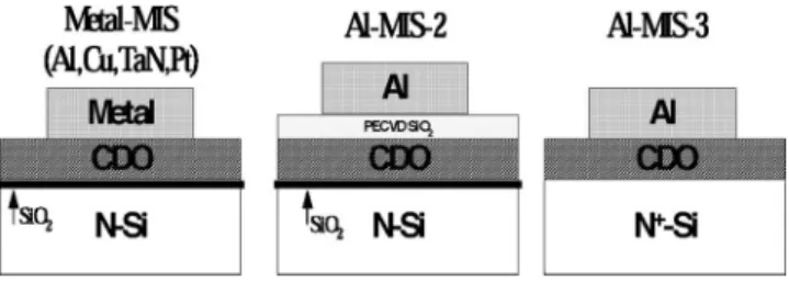
Simple metal-insulator-metal共MIS兲 capacitor structure was used to study the electrical properties of the CDO film. The starting ma-terial was phosphorus-doped共100兲-oriented 8-in. Si wafer with re-sistivity of 2-4⍀ cm. To minimize the influence of interface insta-bility, a 10-nm-thick SiO2 was thermally grown before the deposition of CDO film. The MIS structures are divided into three categories. In the first category, the MIS structure is metal/CDO共200 nm兲/SiO2共10 nm兲/n-Si with various kinds of metal共Al, Cu, TaN, and Pt兲. These samples are denoted as Al-MIS, Cu-MIS, TaN-MIS, and Pt-MIS. All kinds of metal except Al were deposited in a dc sputtering system while Al was deposited in a thermal evaporating system. The second category is a reference
sample with structure of Al共500 nm兲/PECVD
SiO2共30 nm兲/CDO 共200 nm兲/SiO2共10 nm兲/n-Si and is denoted as Al-MIS-2. Because of the existence of thermal oxide and the work-function difference between gate and Si substrate, the above struc-tures are asymmetric. The third category is an almost symmetric MIS structure using an Al gate and heavily doped n-type Si substrate 共less than 0.01 ⍀ cm兲. This structure was fabricated to study the
carrier transport mechanism. The structure is
Al共500 nm兲/CDO 共200 nm兲/n+-Si and is denoted as Al-MIS-3. Figure 1 shows the schematic drawings of the structures of the three categories.
Thin CDO film was deposited in a Trikon Technologies Planar 300 plasma-enhanced chemical vapor deposition system at room temperature using an organo-silane precursor with He as carrier gas.8A 30 min nitrogen gas furnace annealing at 400°C was per-formed before metal gate deposition. A metal mask was use to define gate electrode. A 30-nm-thick SiNx layer was deposited on the
sample surface to protect the dielectric from moisture absorption and to protect the Cu gate from oxidation during storage.
The film thickness and porosity of the deposited CDO film were measured by the ellipsometry method. The atomic composition was determined by Rutherford backscattering spectrometry共RBS兲 analy-sis and the major chemical bonds were identified using electron spectroscopy for chemical analysis共ESCA兲. Fourier-transformed in-frared共FTIR兲 spectroscopy was also employed to evaluate the ma-terial property.
Both capacitance-voltage共C-V兲 and current-voltage 共I-V兲
char-z
acteristics were measured to evaluate the CDO film using a preci-sion impedance meter of model Agilent 4284A and a semiconductor parameter analyzer of model Agilent 4156C, respectively. A bias temperature stress共BTS兲 test under various temperatures and elec-tric fields was performed. Nitrogen gas purge was carried out during device measurement to avoid moisture absorption and metal gate oxidation. Flatband voltages共VFB兲 before and after BTS were ex-tracted from high-frequency共100 kHz兲 C-V characteristic with volt-age swept either from inversion mode to accumulation mode 关for-ward voltage sweep共FVS兲兴 or from accumulation mode to inversion mode关reverse voltage sweep 共RVS兲兴. A time-dependent dielectric breakdown共TDDB兲 test was performed to extract the lifetime of CDO film. CDO dielectric breakdown happened when the stressed capacitor short-circuited.
Results and Discussion
Fundamental properties of CDO film.—Fundamental properties of the CDO film were characterized at first. The dielectric constant of the CDO film calculated from the Al-MIS sample is about 2.2 and apparently reached the level required for the next-generation IMD.7 The CDO is composed of Si, C, O, and H atoms and the atomic ratio is Si:C:O:H⫽ 20.5:14.5:31:34. Film volume porosity is about 20% measured by optical ellipsometer with a pore size of 1-4 nm mea-sured by cross-sectional transmission electron microscopy 共XTEM兲.8
It would be these nanopores that produce the very low dielectric constant with a low carbon content of 14.5%.
Figure 2a depicts the FTIR spectra of the CDO film after anneal-ing in N2ambient at various temperatures. No changes are observed even after annealing at 400°C for 8 h or at 650°C for 30 min. Figure 2b shows that the thickness shrinkage is less than 3% after 650°C annealing, which indicates almost negligible thermal decomposition. The dielectric constant determined by the C-V method increases slightly to 2.3 after annealing at 600°C for 30 min. These results indicate that the thermal stability of CDO is well beyond the re-quirement of the backend process of the line.
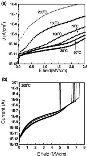
Figure 3a and b shows the current density–electric field共J-E兲 curves of the Al-MIS-3 capacitors at different temperatures and the breakdown characteristic of Al-MIS-3 capacitors at 200°C, respec-tively. The CDO film exhibits very low leakage current density of 1 nA/cm2 at 2.5 MV/cm and room temperature. It also has very high dielectric strength of higher than 5 MV/cm even at 200°C. It is thus concluded that being a porous low-k material, CDO film shows very good thermal stability and very low leakage current.
CDO electrical instability behaviors.—Although CDO film ex-hibits low dielectric constant, high thermal stability, low leakage current, and high dielectric strength, electrical instability was ob-served during the C-V measurement of the Al-MIS sample. By re-peating the C-V measurement on the Al-MIS capacitor at room tem-perature from inversion mode to accumulation mode共FVS兲 and then from accumulation mode to inversion mode共RVS兲, VFBshift with respect to the original C-V curve was observed. The C-V curve shifts toward the positive voltage direction under wide-range FVS with voltage sweeps from −40 to 40 V, while it shifts toward the
negative voltage direction under wide-range RVS with voltage sweeps from 40 to −40 V. The shifts under FVS and RVS are asym-metric and a net shift toward negative voltage direction was ob-served. Figure 4 exhibits the C-V curves of the Al-MIS sample before and after electrical stress at −2 and +2 MV/cm for 4 min. It is also observed that positive electric field stress causes larger VFB shift. All of the metal-MIS capacitors exhibit similar electrical in-stability under continuous C-V measurements. Because of the asym-metric shift, the C-V instability could not be simply explained by the dielectric polarization.20
A BTS test was performed at 30 and 150°C for 30 min. The electric field is 0.6 MV/cm. The magnitudes of VFBshift after BTS are listed in Table I. The magnitudes of VFBshift of the four kinds of MIS capacitors are Al-MIS, Cu-MIS, TaN-MIS, and Pt-MIS in the sequence from high to low. It should be stressed that the magnitude of VFBshift of the Al-MIS sample is even larger than that of the Cu-MIS sample. This observation is totally different from that of the dielectric in silicon dioxide. It is well known that Al is quite stable in contact with SiO2because a very thin self-limiting Al2O3forms between Al and SiO2and acts as a good diffusion barrier.12,13The TaN-MIS and Pt-MIS samples exhibit very slight VFBshift. As the BTS was performed at 150°C, the magnitude of VFBshift is enlarged but the sequence order remains unchanged.
Dielectric polarization phenomenon of CDO film.—There are four possible mechanisms that may cause dielectric C-V instability: 共i兲 the 10-nm-thick thermal oxide is unstable; 共ii兲 the CDO film is Figure 1. Schematic drawings of the MIS structures used in this
work. Metal-MIS: metal/CDO共200 nm兲/SiO2共10 nm兲/n-Si. Al-MIS-2:Al
共500 nm兲/PECVD SiO2共30 nm兲/CDO 共200 nm兲/SiO2共10 nm兲/n-Si. Al
-MIS-3:Al共500 nm兲/CDO 共200 nm兲/n+-Si.
Figure 2. 共a兲 FTIR spectra and 共b兲 thickness shrinkage and dielectric
contaminated by mobile ions such as Na, K, Cu, etc.;共iii兲 the CDO film is polarized under electric field;共iv兲 charges are injected into the CDO film under electric field. In the following discussions, these mechanisms are examined one by one.
The quality of the 10-nm-thick thermal oxide was examined first. A simple Al/SiO2共10 nm兲/Si MOS capacitor was fabricated. The dielectric constant obtained from high-frequency C-V measurement is around 4.0 with a flatband voltage of −0.2 V. No hysteretic phe-nomenon was observed during continuous C-V measurements. Therefore, the instability of the thin thermal oxide is ruled out.
Secondary-ion mass spectrometry 共SIMS兲 analysis of blanket CDO film was performed to detect metal contamination. The mobile ions in CDO film, including Na, K, and Cu, are lower than the detection limit of SIMS analysis. But it had been reported that Al and Cu ions could be driven into CDO film during a BTS test. These metal ions could thermally diffuse along the nanoporous structures. The detailed mechanisms of metal ion drift and thermal diffusion in CDO film were discussed in our previous paper.21The severe VFB shift after BTS of these two kinds of samples can be attributed mainly to the metal ions. However, Pt as a noble metal and TaN being a diffusion barrier metal cannot be driven into CDO film, but the C-V instability phenomenon still occurs. This instability cannot be explained by mobile ions, and another mechanism must be con-sidered. The dielectric polarization is thus examined.
It is known that the VFBshift under continuous FVS and RVS may be attributed to dielectric polarization.20To avoid the influence of metal gate and metal deposition induced damage, the Al-MIS-2 structure with an additional 30-nm-thick PECVD SiO2 between CDO and Al metal gate was used to study the role of dielectric polarization on the electrical instability. Silicon dioxide is known to be a good diffusion barrier of Al metal ions, and Al ions cannot drift across it.12,13,21The stable C-V characteristics of reference sample Al/PECVD SiO2/thermal SiO2/Si structure indicate that both the PECVD SiO2film and the metallization process are well controlled. Figure 5 shows the high-frequency C-V characteristics of Al-MIS-2 measured in both of the FVS and RVS modes for two cycles. The original curve was measured in the FVS mode with voltage Figure 3.共a兲 Current density-electric field characteristic of Al-MIS-3 sample
measured at different temperatures.共b兲 The breakdown characteristics of Al-MIS capacitors at 200°C.
Figure 4. Capacitance-voltage curves of Al-MIS sample after electrical
stress at 150°C −2 and +2 MV/cm for 4 min.
Figure 5. Capacitance-voltage curves of Al-MIS-2 sample with different
swept from −20 to +10 V. The original C-V curve looks like a normal C-V curve of a typical MIS capacitor. However, as the volt-age range is expanded to ±40 V, the C-V curve shifts apparently. In the FVS mode, the C-V curve shifted toward the positive voltage axis, while in the RVS mode, the C-V curve shifted toward the negative voltage axis. The magnitudes of VFBshift in both directions are almost identical and the C-V curves are almost overlapped in continuous FVS and RVS measurement cycles. Because the electric field is only about 1.6 MV/cm共40 V/240 nm兲, the VFBshift cannot be explained by electrons共or holes兲 injection from either gate or substrate through the SiO2 layer. Therefore, the VFB shift of the Al-MIS-2 sample could be attributed to dielectric polarization.20
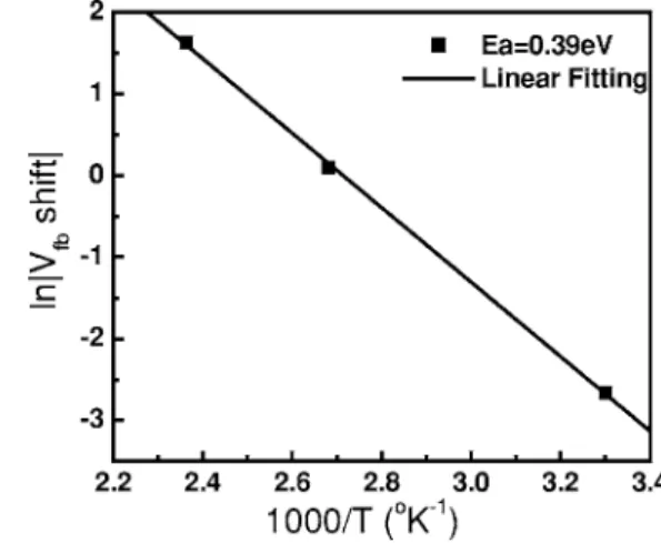
The Al-MIS-2 capacitor was electrically stressed at 0.6 MV/cm for 30 min. The VFBshifts of the Al-MIS-2 sample stressed at 30 and 150°C are −0.07 and −5.12 V, respectively. The C-V curves are shown in Fig. 6a and b. The negligible VFBshift of the Al-MIS-2 sample at 30°C indicates that the CDO film is electrically stable at room temperature. Figure 7 shows the Arrhenius plot of the magni-tude of VFBshift at 0.6 MV/cm. The extracted activation energy for dielectric polarization is 0.39 eV. It is observed that CDO film might cause VFBshift more easily under higher-temperature stress condi-tion. Besides, it is observed that the VFB shift of TaN-MIS and Pt-MIS capacitors is slightly larger than the dielectric polarization induced VFBshift, therefore an additional mechanism must be con-sidered.
Carrier injection in CDO dielectric.—Although the dielectric polarization of CDO film can be used to explain the symmetric C-V shift under electric field and mobile ions can be used to explain the large VFBshift under positive voltage stress with some kinds of metal electrode, there is still another possible mechanism that may cause VFBshift, namely carrier injection and trapping in CDO film. For metal-MIS samples biased at low electric field such as +0.6 MV/cm, it is hard for an electron to be injected from the Si substrate across thermal oxide into CDO film. Hole injection from the metal gate into CDO film is also unlikely. As metal-MIS samples are biased at −0.6 MV/cm, it is still hard for the hole to be injected from the Si substrate across thermal oxide into CDO film, but it is possible for an electron to be injected from the metal gate into CDO film. To study the carrier transport mechanism, the Al-MIS-3 sample with a nearly quasi-metal-insulator-metal 共MIM兲 structure of Al/CDO/N+-Si was fabricated. Figure 8a shows that the J-E char-acteristic at low temperature or low electric field can be well fitted with the Schottky emission共SE兲 model. At high temperature or high electric field, the J-E characteristic could be better fitted with the Frenkel-Poole共FP兲 model, as shown in Fig. 8b. The transition elec-tric field from Schottky emission to Frenkel-Poole emission de-creases with the increase of temperature.
Because FP emission is due to field-enhanced thermal excitation of trapped electrons into the conduction band, and the barrier height is the depth of the trap potential well, it is expected that FP emission can occur at lower electric field than Schottky emission. If the low field tunneling mechanism is Schottky emission, it is unreasonable for FP emission to dominate carrier transport at high field. Thus, the observation of Schottky emission at low electric field and FP emis-sion at high temperature is unusual for dielectrics. To explain this phenomenon, the role of Al gate must be considered. It is postulated that the transition of the carrier transport mechanism might be at-tributed to the Al ions induced defects in bulk CDO. As has been reported in our previous paper, Al ions can be driven into CDO film by electric field.21These Al ions produce trap sites there. More Al ions are driven into CDO film at higher temperature. Therefore, the trap site density increases with the increase of electric field and measurement temperature, and then the carrier transport mechanism changes from Schottky emission to FP emission at high electric field and the transition field decreases with the increase of temperature. This postulation is further verified by the measurement results of the Al-MIS-2 sample. Because of the capped thin PECVD SiO2layer on CDO film, Al ions cannot enter the bulk CDO. Figure 9 shows that the J-E characteristics of Al-MIS-2 at negative bias can be fitted with the Schottky emission model at high electric field even at 200°C.
Now the observed electrical instability can be understood with the model proposed in Fig. 10. Weak dielectric polarization occurs Figure 6. Capacitance-voltage curves result of Al-MIS-2 sample after BTS
at共a兲 room temperature and 共b兲 150°C. The electric field is 0.6 MV/cm.
under electric field at high temperature. If CDO film contacts with metal directly, electrons may be injected from the metal gate as the gate is negatively biased. Both dielectric polarization and electron injection cause slight VFB shifts toward positive voltage direction. Because the leakage current of CDO film is very low, electron in-jection can be neglected at a typical operation condition of less than 0.2 MV/cm. As the gate is positively biased, metal ions such as Cu and Al would be driven into the porous CDO film. The positive
metal ions result in a large VFBshift toward the negative voltage direction. Combined with CDO dielectric polarization phenomenon, VFBshifts dramatically.
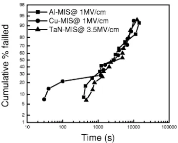
Electrical reliability study of CDO film.—The time-dependent dielectric breakdown 共TDDB兲 of Al-MIS, Cu-MIS, and TaN-MIS capacitors was evaluated at 1a, 1, and 3.5 MV/cm, respectively. Figure 11 shows the cumulative failure plot at a temperature of 200°C. It is observed that the lifetimes of the three kinds of samples are very close. Because the electric field of the TaN-MIS sample is much stronger than that of the other two samples, the lifetime of the TaN-MIS sample is much longer than that of the other two samples. It is known that no metal ions were driven into CDO films for the TaN-MIS sample. The long lifetime of the TaN-MIS sample reflects the actual reliability of the CDO film. As discussed in the preceding section, metal ions trapped in CDO film produce traps so that the carrier injection mechanism changes from Schottky emission to FP emission. It is also known that the TDDB lifetime is strongly related to defect density. The short lifetime of the Al-MIS sample and the Cu-MIS sample should be related to the injection of Al ions and Cu ions, respectively, into CDO film during the TDDB test.
It is known that the carrier transport mechanism at electric field lower than 10 MV/cm of the CDO film is Schottky emission but not FN emission and the CDO film is thick enough. It is supposed that the TDDB lifetime of the CDO film follows the E-model.22-24Figure Figure 8. The J-E characteristic of Al-MIS sample can be well fitted by共a兲
the Schottky emission model at low temperature and low electric field, and 共b兲 the Frenkel-Poole model at high temperature and high electric field.
Figure 9. The J-E characteristic of Al-MIS-2 sample at negative gate voltage
can be well fitted by the Schottky emission model from room temperature to 200°C.
Figure 10. Proposed model to explain the observed electrical instability of
metal-MIS capacitors.
Figure 11. Cumulative TDDB failure of Al-MIS, Cu-MIS, and TaN-MIS
samples stressed at 1, 1, and 3.5 MV/cm, respectively. The temperature is 200°C.
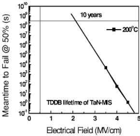
12 shows the mean time to failure共MTTF兲 of the TaN-MIS sample as a function of electric field at 200°C. The 10-year MTTF allows an electric field of stronger than 2 MV/cm, and the extrapolated MTTF at electric field of 0.5 MV/cm is much longer than 10 years by several orders of magnitude. These results indicate that the reliabil-ity of CDO film without metal contamination is well beyond the requirement of multilevel interconnection, and that TaN, the com-monly used Cu diffusion barrier metal, is fully compatible with the CDO film.
Conclusions
In this work, the electrical instability of nanoporous carbon-doped oxide film was studied for the first time. Excellent basic prop-erties including low dielectric constant共lower than 2.3兲 after anneal-ing at 600°C, good thermal stability共no FTIR spectrum change after annealing at 650°C兲, very little thickness shrinkage 共less than 3% after annealing at 650°C兲, and low leakage current 共lower than 1 nA/cm2at 30°C and 2.5 MV/cm兲 are confirmed in this work.
However, in order to integrate CDO film into the complicated integrated circuits, the electrical stability and reliability must be evaluated carefully. In this work, an electrical instability model con-sidering metal ion diffusion, dielectric polarization, and carrier in-jection was proposed to explain the observed electrical instability phenomenon of the CDO film under electrical stress. It is concluded that Al and Cu are not suitable metals to contact with CDO film directly because Al ions and Cu ions can be driven into CDO film easily. Fortunately, TaN, a barrier metal for the Cu-interconnect sys-tem, shows no mobile ion issues when in direct contact with CDO film. The electron transport mechanism is identified to be Schottky emission at low electric field and low temperature. As metal ions are injected into CDO film, for example Al and Cu, the electron trans-port mechanism changes to Frenkel-Pool emission at high tempera-ture and high electric field. The injection of metal ions into CDO film also degrades the TDDB lifetime of the film. Fortunately, the
commonly used Cu diffusion barrier TaN is an excellent contact metal with CDO film. The 10-year TDDB lifetime allows an electric field stronger than 2 MV/cm and the TDDB lifetime at 0.5 MV/cm becomes longer than 10 years by several orders of magnitude. It is thus concluded that the nanoporous ultralow dielectric constant CDO film is a very promising intermetal dielectric material for next-generation interconnect systems.
Acknowledgments
The authors express their great appreciation to Knut Beemann, Tony Wilby, Kath Giles, and Sajid Ishaq at Trikon Technologies, U.K. for samples preparation. This work is partially supported by the National Science Council, ROC under contract no. NSC92-2215-E-009-001.
National Chiao-Tung University assisted in meeting the publication costs of this article.
References
1. S. Bothra, B. Rogers, M. Kellam, and C. M. Osburn, IEEE Trans. Electron
De-vices, 40, 591共1993兲.
2. S. Wolf and R. N. Tauber, Lattice Press, pp. 181-199, Sunset Beach, CA共1986兲. 3. T. Sakurai, IEEE Trans. Electron Devices, 40, 118共1993兲.
4. B. K. Liew, P. Fang, N. W. Cheung, and C. Hu, IEEE Trans. Electron Devices, 39, 2472共1992兲.
5. J. Tao, K. K. Young, N. W. Cheung, and C. Hu, IEEE Trans. Electron Devices, 44, 1398共1993兲.
6. K. Ueno, K. Ohto, and K. Tsunenari, Symposium on VLSI Technology, Digest of
Technical Papers, IEEE, p. 27共1995兲.
7. SIA International Technology Roadmap for Semiconductors, Semiconductor Indus-try Association, San Jose, CA共2001兲.
8. K. Buchanan, K. Beekmann, K. Giles, J.-C. Yeoh, and H. Donohue, Proceedings of
the Advanced Metallization Conference, MRS, p. 73共2001兲.
9. S. Nozaki, S. Banerjee, K. Uchida, H. Ono, and H. Morisaki, IEEE International
Interconnect Technology Conference, p. 140共2000兲.
10. Chanming Jin and Jeff Wetzel, in IEEE International Interconnect Technology
Conference, pp. 99-101共2001兲.
11. A. L. S. Loke, J. T. Wetzel, C. Ryu, W. J. Lee, and S. S. Wang, Symposium on VLSI
Technology, Digest of Technical Papers, IEEE, p. 26共1998兲.
12. A. L. S. Loke, J. T. Wetzel, P. H. Townsend, T. Tanabe, R. N. Vrtis, M. P. Zussman, D. Kumar, C. Ryu, and S. S. Wong, IEEE Trans. Electron Devices, 46, 2178 共1999兲.
13. A. Mallikarjunan, S. P. Murarka, and T. M. Lu, Appl. Phys. Lett., 79, 1855共2001兲. 14. A. Jain, S. Rogojevic, S. Ponoth, N. Agarwal, I. Matthew, W. N. Gill, P Persans, M. Tomozawa, J. L. Plawsky, and E. Simonyi, Thin Solid Films, 398-399, 513 共2001兲.
15. M. Tada, Y. Harada, K. Hijioka, H. Ohtake, T. Takeuchi, S. Saito, T. Onodera, M. Hiroi, N. Furutake, and Y. Hayashi, IEEE International Interconnect Technology
Conference, pp. 12-14共2002兲.
16. J. C. Lin, R. Augur, S. L. Shue, C. H. Yu, M. S. Liang, A. Vijayendran, T. Suwwan de Felipe, and M. Danek, IEEE International Interconnect Technology Conference, p. 21共2002兲.
17. H. J. Lee, Y. H. Kim, J. Y. Kim, E. K. Lin, B. J. Bauer, W. l. Wu, and H. J. Kim,
IEEE International Interconnect Technology Conference, p. 54共2002兲.
18. C. Waldfried, Q. Han, O. Escorica, A. Margolis, R. Albano, and I. Berry, IEEE
International Interconnect Technology Conference, p. 226共2002兲.
19. K. L. Fang, B. Y. Tsui, C. C. Yang, M. C. Chen, S. D. Lee, K. Beekmann, T. Wilby, K. Giles, and S. Ishaq, IEEE International Interconnect Technology Conference, pp. 60-63共2002兲.
20. B. Y. Tsui, K. L. Fang, and S. D. Lee, IEEE Trans. Electron Devices, 48, 2375 共2001兲.
21. Kuo-Lung Fang and Bing-Yue Tsui, J. Appl. Phys., 93, 5546共2003兲. 22. J. W. McPeherson and H. C. Mogul, J. Appl. Phys., 84, 1513共1998兲.
23. K. C. Boyko and D. L. Gerlach, International Reliability Physics Proceedings, IEEE, p. 7共1989兲.
24. K. F. Schuegrapf and Chenming Hu, International Reliability Physics Proceedings, IEEE, p. 7共1993兲.
Figure 12. Extrapolation of TDDB lifetime of TaN-MIS sample at 200°C