國 立 交 通 大 學
電信工程學系
碩士論文
新式的多模諧振腔濾波器
Novel Multiple-mode Resonator Filters
研究生:林逸亭
指導教授:張志揚 博士
新式的多模諧振腔濾波器
Novel Multiple-mode Resonator Filters
研 究 生:林逸亭
Student:Yi-Ting Lin
指導教授:張志揚 博士 Advisor:Dr. Chi-Yang Chang
國立交通大學
電信工程學系
碩士論文
A Thesis
Submitted to Department of Communication Engineering
College of Electrical and Computer Engineering
National Chiao Tung University
In Partial Fulfillment of the Requirements
for the Degree of
Master of Science
In
Communication Engineering
June 2008
Hsinchu, Taiwan, Republic of China
中華民國 九十七 年 六 月
新式的多模諧振腔濾波器
研究生:林逸亭 指導教授:張志揚 博士
國立交通大學電信工程學系
摘要
本篇論文提出ㄧ種新式的多模態諧振腔濾波器,其主要的特點是具有一個可 調整的傳輸零點和大範圍的上止帶,設計方法是將濾波器的諧振頻率調到與 Chebyshev 通帶的傳輸極點相同位置,當我們將耦合量增強,便可產生一個形似 Chebyshev 的頻率響應,可調的傳輸零點由傳輸零點頻率的四分之一波長開路支 線傳輸線產生,且此開路支線傳輸線並聯一個電抗,即決定傳輸零點出現在下止 帶或上止帶,本篇中有三個 2.45GHz 三模態諧振腔濾波器的設計,量測結果皆與 模擬相符合。 本篇有另一個濾波器設計方法是使用中間為並聯電抗或串連電納,兩邊為 阻抗不相等傳輸線,所形成的 K 倒反器或 J 倒反器來合成濾波器,傳統的方法 是使兩邊的傳輸線阻抗相等,因此,我們的設計更為靈活。我們將重點放在 K 倒反器上,J 倒反器可同理推得,跟上ㄧ個主題相仿,此處也有ㄧ個由傳輸零 點頻率的λ/4 開路支線傳輸線所產生的可調傳輸零點,此傳輸線可視為並聯電 抗,在兩端加上兩段不同度數、不同阻抗的傳輸線,等效成一個 K 倒反器,本 篇中實作兩個 2.45GHz 的三階濾波器以驗證理論。Novel Multiple-mode Resonator Filters
Student: Yi-ting Lin Advisor: Dr. Chi-Yang Chang
Department of Communication Engineering
National Chiao-Tung University
Abstract
Novel planar bandpass filters with a configurable finite transmission zero and wide upper stop-band are synthesized based on multimode resonator property. The resonances of the resonators are tuned to match the transmission poles of a Chebyshev pass-band in order to create Chebyshev-like response while enhancing the coupling. The transmission zero at finite frequency is brought about by a open-circuit stub with quarter-wavelength of zero frequency. Additionally, the open-circuit stub connecting a shunt reactance can be used to allocate that the transmission zero in the lower or the upper stopband. Tri-mode bandpass filters with the transmission zero on the different sides of the passband are designed. The measured results both show good agreement with simulated responses.
Another design included in this article is the filter with K or J inverter making use of unequal impedance microstip lines with shunt reactance or series susceptance in between. It’s more flexible and much different from the conventional design having equal impedance microstrip lines on the both sides. We discuss the K inverter design
only since the design guidelines are the same as those of the J inverter. A centered open-circuit stub is taken to be the reactance and utilized to tune transmission zero position. Third-order band-pass filters with transmission zeros on the different sides of the passband are designed and measured to validate the approach.
誌謝
首先必須感謝指導教授張志揚博士,在兩年的碩士生涯中,給予適時的教導 與指引,幫助我們完成論文,平時也跟我們ㄧ同用餐、爬山,有如朋友ㄧ般,能 有這樣的良師益友,真是我的一大福氣。 當然也要感謝學長跟同學們,小谷、雄哥、哲慶、建育、梁八幾位實驗室的 學長,在研究上給予許多的提點,錞哥、銘哥、威綸、智皓、憲文這些同窗們, 互相勉勵在實驗室度過了兩年,巴里、雅惠、郁文、阿冷讓我當了很久女二 484 的偽室友,還有菁偉、澎澎、小花、useful 等 912 的朋友們,一起吃吃喝喝到 處玩,絕對不能漏掉的是小胖,不但容忍我的任性和壞脾氣,要當我的車伕,還 教我排版軟體怎麼用,我才可以把論文很漂亮的呈現出來。 最後要謝謝我的家人,親愛的爸爸永遠都給予最大的鼓勵和支持,常常幫我 準備ㄧ些補品,,媽媽和外婆在天堂裡,ㄧ定也有為我禱告,最希望看我拿到碩 士的奶奶雖然在口試前幾週不幸過世,但我相信她在天上也能感受到這份喜悅, 還有三位姐姐葳亭、憶君、珍瑜的疼愛,也讓我溫暖在心頭,只能說是大家滿滿 的愛,讓我順利的完成碩士論文。Contents
1 Introduction 1
1.1 Motivation . . . 1
1.2 Introduction to Multimode Resonator Filter . . . 1
1.3 Introduction to J and K inverter . . . 2
1.4 Introduction to Wireless LAN . . . 3
2 Multimode Resonator Filters 5 2.1 Previous Works of Multimode Resonator Filters . . . 5
2.2 Design Procedure of Multimode Resonator Filter . . . 8
2.3 Proposed Multimode Resonator Filters . . . 9
2.3.1 Tri-mode Resonator Filter with Upper-Stopband Transmission Zero 10 2.3.2 Tri-mode Resonator Filter with Lower-Stopband Transmission Zero 20 2.3.3 Comparison of the Filter with Upper-Stopband Transmission Zero and the Filter with Lower-Stopband Transmission Zero . . . 32
3 J and K Inverter Filters 34
3.1 Filters with Ideal J and K inverters . . . 34
3.1.1 Low-pass Prototype Filter . . . 34
3.1.2 Low-pass Prototype Filter to Band-pass Filter Transformation . . 36
3.2 Symmetric J and K Inverter Filters . . . 38
3.3 Asymmetric J and K Inverter Filters . . . 41
3.3.1 K Inverter Filter with Upper-Stopband Transmission Zero . . . . 46
3.3.2 K Inverter Filter with Lower-Stopband Transmission Zero . . . . 51
List of Figures
1-1 Basic operation of K inverter . . . 2
1-2 Basic operation of J inverter . . . 3
1-3 Protocals of 802.11 . . . 4
2-1 Geometry of a SIR with Z2>Z1 . . . 7
2-2 Design ‡ow chart of MMR …lters . . . 8
2-3 Structure of tri-mode resonator with positive jX . . . 11
2-4 Three resonators of tri-mode resonator with positive jX . . . 11
2-5 Zero controller of tri-mode resonator with positive jX . . . 11
2-6 Simulated schematic circuit with loose coupling in AWR . . . 13
2-7 E¤ect of the impedance of short-circuit stub(Zshort) on resonant frequencies 13 2-8 E¤ect of the length of short-citcuit stub( short) on resonant frequencies . 14 2-9 E¤ect of the impedance of open-circuit stub(Zopen) on resonant frequencies 14 2-10 Simulated schematic circuit of tri-mode …lter with an upper-stopband transmission zero in AWR . . . 16
2-11 Simulated frequency response of tri-mode …lter with an upper-stopband transmission zero in AWR . . . 16
2-12 Simulated physical layout of tri-mode …lter with an upper-stopband trans-mission zero in Sonnet . . . 17
2-13 Simulated frequency response of tri-mode …lter with an upper-stopband transmission zero in Sonnet . . . 17
2-15 Measured frequency response of tri-mode …lter with an upper-stopband
transmission zero(narrow band) . . . 18
2-16 Measured frequency response of tri-mode …lter with an upper-stopband transmission zero(wide band) . . . 19
2-17 Structure of tri-mode resonator …lter with negative jX . . . 20
2-18 Three resonators of tri-mode resonator …lter with negative jX . . . 21
2-19 Zero controller of tri-mode resonator …lter with negative jX . . . 21
2-20 Simulated schematic circuit with loose coupling in AWR . . . 22
2-21 E¤ect of the impedance of open-circuit stub(Zopen) on resonant frequencies 23 2-22 E¤ect of capacitor(C) on resonant frequencies . . . 23
2-23 Simulated schematic circuit of tri-mode …lter with strong coupling with a lower-stopband transmission zero in AWR . . . 25
2-24 Simulated frequency response of tri-mode …lter with a lower-stopband transmission zero in AWR . . . 25
2-25 Photograph of the tri-mode …lter with a lower-stopband transmission zero using a lumped capacitor . . . 26
2-26 Measured frequency response of tri-mode …lter with a lower-stopband transmission zero using a lumped capacitor (narrow band) . . . 26
2-27 Measured frequency response of tri-mode …lter with a lower-stopband transmission zero using a lumped capacitor(wide band) . . . 27
2-28 Simulated physical layout of tri-mode …lter with a lower-stopband trans-mission zero using a patch capacitor in Sonnet . . . 29
2-29 Simulated frequency response of tri-mode …lter with a lower-stopband transmission zero using a patch capacitor in Sonnet . . . 29
2-30 Photograph of the tri-mode …lter with a lower-stopband transmission zero using a patch capacitor . . . 30
2-31 Measured frequency response of tri-mode …lter with a lower-stopband transmission zero using a patch capacitor(narrow band) . . . 30
2-32 Measured frequency response of tri-mode …lter with a lower-stopband
transmission zero using a patch capacitor(wide band) . . . 31
2-33 Low stop-band rejection ability of the tri-mode …lter with an upper-stopband transmission zero . . . 33 2-34 Low stop-band rejection ability of the tri-mode …lter with a lower-stopband
transmission zero . . . 33
3-1 Low-pass prototype . . . 34
3-2 De…nition of gk . . . 35
3-3 The gk of Chebyshev reponse with pass-band ripple level =0.01dB . . . . 35
3-4 Using K inverter to change shunt capacitors to series inductors . . . 36
3-5 Transform LPF to BPF . . . 37
3-6 J and K inverters . . . 38
3-7 K inverters implementation with equal impedance transmission lines
be-sides the shunt reactance . . . 39
3-8 J inverters implementation with equal impedance transmission lines
be-sides the series susceptance . . . 39
3-9 K inverters implementation with unequal impedance transmission lines
besides the shunt reactance . . . 41
3-10 J inverters implementation with unequal impedance transmission lines be-sides the series susceptance . . . 42
3-11 Network of third order …lter with proposed K inverter . . . 44
3-12 Alternative network of third order …lter with proposed K inverter . . . . 45
3-13 Zopen, 1,and 2 varying with Z2 at fz= 2.464GHz . . . 46 3-14 Variation of Zopen with Z2 at fz= 2.464GHz . . . 47 3-15 Simulated schematic circuit of third-order K inverter …lter with an
upper-stopband transmission zero in AWR . . . 47
3-16 Simulated frequency response of third-order K inverter …lter with an
3-17 Simulated physical layout of third-order K inverter …lter with an
upper-stopband transmission zero in Sonnet . . . 48
3-18 Simulated frequency response of third-order K inverter …lter with an
upper-stopband transmission zero in Sonnet . . . 49
3-19 Photograph of third-order K inverter …lter with an upper-stopband trans-mission zero . . . 50 3-20 Measured frequency response of third-order K inverter …lter with an
upper-stopband transmission zero . . . 50 3-21 Zopen, 1,and 2 varying with Z2 at fz= 2.254GHz . . . 51 3-22 Variation of Zopen with Z2 at fz= 2.254GHz . . . 52 3-23 Simulated schematic circuit of third-order K inverter …lter with a
lower-stopband transmission zero in AWR . . . 52
3-24 Simulated frequency response of third-order K inverter …lter with a
lower-stopband transmission zero in AWR . . . 53
3-25 Simulated physical layout of third-order K inverter …lter with a
lower-stopband transmission zero in Sonnet . . . 54
3-26 Simulated frequency response of third-order K inverter …lter with a
lower-stopband transmission zero in Sonnet . . . 54
3-27 Photograph of third-order K inverter …lter with a lower-stopband trans-mission zero . . . 55 3-28 Measured frequency response of third-order K inverter …lter with a
Chapter 1
Introduction
1.1
Motivation
My interest in multimode resonator …lter comes from some of its attractive features such as compact planar structure, high selectivity, and simple design guidelines, which are essential for applications in rapidly growing wireless communications. Hence, papers relative to the subject have been studied in this thesis. The foundation of multimode resonator …lter designing rules has been established by the predecessors, that is, we could follow the way they paved for us. However, we need to indicate our originality by advancing a brand-new idea.
1.2
Introduction to Multimode Resonator Filter
MMR …lter is abbreviated from Multiple-mode Resonator Filter. Recently, a lot of re-searches involved MMR …lters have been published. Its main concept is gathering several resonant modes of the resonator to form the pass-band. As a result, we …rst need to …nd an appropriate circuit that can contribute two or more resonances at di¤erent frequen-cies. Plurality of the presented paper chose the stepped-impedance resonator (SIR) as
the bulk of the …lter due to its versatile resonant characteristics. Its resonant frequencies can be easily altered by tuning its geometric parameters. However, instead of stepped-impedance resonator,we provide a novel resoantor structure to implement multimode resonator …lters. For further details, one can refer to Chapter 2.
1.3
Introduction to J and K inverter
As we all know that it is often desirable to have all series or all shunt elements in …lter implementation. We can use impedance (K) inverters or admittance (J) inverters to do the job. J and K inverters are useful for band-pass or band-stop …lters especially with narrow bandwidths(<10%). Fig. 1-1 and 1-2 are the basic operation of impedance and admittance inverters. Concerning about the K inverter in the graph, if the load has positive reactance (inductors), it will seem to have negative reactance (capacitors) at the output by inserting the K inverter. There are many types of network to realize J and K inverters. One of the commonly used network is a shunt impedance for a K-inverter or a series admittance for a J-K-inverter where two equal characteristic impedance transmission line resonators locate on each side of the inverter. The design formulas are well developed[12] for these inverters. Here, we developed design formulas for two resonators with di¤erent characteristic impedances. Our discussion brie‡y starts from the here and will be completed in the Chapter 3.
ZL
K + 90° Zin=K2/ZL
YL J + 90° Yin=J 2 /YL
Figure 1-2: Basic operation of J inverter
1.4
Introduction to Wireless LAN
A wireless LAN or WLAN is short for wireless local area network, which links two or more computers without using wires. This gives users the ability to move around within a broad coverage area and still be connected to the network.
For the home user, wireless has become popular due to ease of installation, and location freedom with the gaining popularity of laptops. Many co¤ee shops or malls have begun to o¤er wireless access to allure their customers. Thus, large wireless network business is being put up in many cities.
The majority of computers sold to consumers today come pre-equipped with all nec-essary wireless LAN technology because of their convenience, cost e¢ ciency, and ease of integration with other networks. However, wireless LANs may have some limitations about security, range, reliability, and speed for a given networking situation.
The IEEE standard that regulates WLAN technology is IEEE 802.11 which has gone through several generations since 1997. Some protocol of 802.11 that their products have been available in the market are summarized as follows,
Figure 1-3: Protocals of 802.11
Evidently, the 2.4 GHz ISM band is very popular for use. In consequence, most of our experiment have made in 2.4 GHz band foreseeing their future applications.
Chapter 2
Multimode Resonator Filters
2.1
Previous Works of Multimode Resonator Filters
The method of design …lters using multimode cavity initially appeared in [2] that the …rst two resonant modes of the MMR together with enhanced I/O parallel-coupled lines will construct wide pass-band with four transmission poles. In [3], the …rst three res-onant modes of an MMR has been newly utilized to construct the pass-band with …ve transmission poles. Basically following the work in [2] and [3], MMRs in [4]-[6] were properly modi…ed in con…guration in order to match its …rst three resonant modes to the lower-end, center, and upper-end of the desired pass-band. When coupling degree of the input/output parallel coupled lines is boosted, good pass-band performance are realized. Setting up the coupling peak of quarter-wavelength parallel coupled lines at the center frequency, the three types of planar band-pass …lters were implemented on the traditional microstrip line[4],on aperture-backed microstrip line[5], and on hybrid microstrip/CPW[6]. Five pole …lters can be synthesized with a single triple-mode SIR and an excitation structure with strong coupling. The impedance junctions between SIR and the excitation structure may create two more transmission poles.
However, the researches mentioned before didn’t have a systematical design procedure. Not until the MMR reported in [7] was proposed could we follow the clear design guideline. The paper developed a systematical procedure for synthesizing broadband band-pass …lters using single or plural multiple-mode SIRs. For plural multiple-mode SIRs design, each SIRs is viewed as a multiple-mode resonator which contribute two or three resonant modes to the circuit. The resonances of coupled SIRs are tuned to match the transmission poles of a Chebyshev pass-band. By adding appropriate input/output coupling, the BPFs will have a quasi-Chebyshev response. Up to the present, the geometry in Fig. 2-1 of the SIRs with desired resonant spectrum can be obtained by the Eq. 2.1(odd mode) and Eq. 2.2(even mode). The center frequency of a triple-mode SIR is at its second resonance, while that of a dual-mode SIR is at the arithmetic mean of two resonances.
tan 1 = cot 2 (2.1)
cot 1 = R tan 2 (2.2)
where R = Z2/Z1 is the impedance ratio and 1 and 2 are electrical lengths of the
2 θ 2 θ θ1 θ1 2 Z 1 Z Z1 1 Z
Figure 2-1: Geometry of a SIR with Z2>Z1
We calculate the corresponding resonant frequencies by the Eq. 2.3, 2.4, and 2.5.The insersion loss function of a kth-order Chebyshev …lter can be expressed as
jS21j 2
= 1 + jTk(x)j 2
(2.3)
where Tk(x) is the kth-order Chebyshev polynomial of the …rst kind and speci…es
the pass-band ripple level. The frequencies corresponding to jxnj = 0 and 1 are center
frequency and band edges, respectively. The kth-order poles in the equation are given as
xn= cos(
2k + 1 2n
2k ); n = 1; 2; ::::; k (2.4)
For a kth-order Chebyshev BPF with fractional BW , we can calculate the pole
frequencies
fn fo
= 1 + xn
2 (2.5)
where fo is the center frequency.
Once we obtained the pole frequencies, the geometry of the SIR can be chosen to match the resonant frequencies with these transmission poles. It is assumed that I/O feeders do not shift the split-o¤ frequencies signi…cantly.
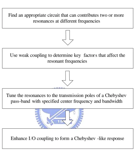
2.2
Design Procedure of Multimode Resonator
Fil-ter
Fig. 2-2 depicts the design ‡ow chart of the MMR …lters summarized from the above,
Find an appropriate circuit that can contributes two or more resonances at different frequencies
Use weak coupling to determine key factor s that affect the resonant frequencies
Tune the resonances to the transmission poles of a Chebyshev pass-band with specified center frequency and bandwidth
Enhance I /O coupling to form a Chebyshev -like response
Figure 2-2: Design ‡ow chart of MMR …lters
Obviously, the design procedure mentioned above is very simple. That is why it wins acceptance among the …lter design methods in the recent years. The …rst step is the most important. If we decide to use the framework that can not contribute resonances at desired frequencies or not easily be tuned by changing geometric parameter, it will lead to a failure in the end. Therefore we must choose our structure carefully. Next step is to …nd critical parameters that dominate the resonances. To ease the simulation, we should
…x some parameters and tune others to meet our goal, matching the resonances the trans-mission poles of a Chebyshev pass-band with speci…ed center frequency and bandwidth. The last but not the least, adding appropriate input/output coupling structure, usually coupled lines, will construct the Chebyshev-like response with slight deviation form the Chebyshev poles. Eventually, the design is realized step by step. The rest of the work is to test and verify.
2.3
Proposed Multimode Resonator Filters
We start our research also according to the guidelines from the previous works. Firstly,
we innovate a new structure which can be regarded as three parts- a c/2(a half
wave-length of center frequency) microstrip line in the middle, a z/4(a quarter wavelength
of transmission zero frequency) open-circuit stub, and a shunt reactance on the opposite side. The shunt reactance can be a short section of short-circuit stub, a patch capacitor, or a lumped circuit capacitor. The con…guration of the circuit is like a cross. The idea
comes from the T-shaped circuit with a c/2 microstrip line in the middle and a c/4
open-circuit stub. T-shaped circuit only has two resonances occurring nearby. Also,
there were cross shaped networks with a c/2 microstrip line in the middle and two c/4
short-circuit stub on the opposite side that have been exploited before[10]. Whatever, two c/4 microstrip line on the each side may occupy large space. As a result, it inspires us to create the design which has three resonances each adjoining to others and simulta-neously reduces the size by using small short-circuit stub, patch, or lumped capacitor to
replace the c/4 stub.
Three kinds of tri-mode resonators are proposed. Each has three neighboring reso-nances and has a upper- or lower-stopband transmission zero. We regarded a small short-circuit stub as an shunt inductance leading to a transmission zero on upper-stopband. If we change the sign of the shunt reactance by replacing the short-circuit stub with a
capacitor, we can have a lower-stopband transmission zero. However, the frequency of the transmission zero is mainly decided by the electrical length of open-circuit stub.
In this paper, all circuits are implemented on a substrate with "r=3.58 and thick-ness=0.508 mm. Before the I/O coupling structure are equipped, the transmission poles are detected by a loose coupling scheme.
2.3.1
Tri-mode Resonator Filter with Upper-Stopband
Trans-mission Zero
Fig. 2-3 shows the basic structure of the proposed resonator. Look deep into the struc-ture, it can be sepapated into three resonators as depicted in Fig. 2-3. These three resonators contribute three distinct but adjacent resonant frequencies. Although, look-ing separately, three resonators have only two resonant frequencies, they are coupled to one another through the shunt reactance and the resonant frequencies are split into three frequencies. The …lter described in this section has positive shunt reactance(inductive), z/4 is electrically shorter than the three resonators. For the reason, the transmission zero’s frequency, which is controlled by z/4 open-circuit stub, falls above three resonant frequencies of the …lter. That is, there is a transmission zero in the upper stop-band. An expression for the above discussion is presented in Fig. 2-4 and Fig. 2-5. On the other hand, if the reactance becomes negative(capacitive), the electrical lengths of the
resonators are shorter than that of c/4 and z/4. And the transmission zero occurs
in the lower stop-band instead. In this section, we use a small short-circuit stub to implement the shunt inductive reactance. It can be derived from the Eq. 2.6,
Zin= jZ0tan l (2.6)
+jX
2
1 3
λc/4 λc/4
λz/4
Figure 2-3: Structure of tri-mode resonator with positive jX
+jX +jX
1 2 3
+jX λz/4
λc/4 λc/4
Figure 2-4: Three resonators of tri-mode resonator with positive jX
λz/4
2
Open
Short
The …lter in this thesis is di¤erent from the single SIR …lter mentioned before. Our design has exactly three resonators, while the single SIR …lter only has one resonator. SIR is trying to pull the second or third harmonic terms into the pass-band. The action has the possiblity that the spurious frequency may be pulled close to the pass-band at the same time unless there are special mechanisms for cancellation. However, the …lter proposed here will have spurious frequency at almost three times above the center frequency.
After deciding the con…guration, we use weak coupling to …nd the key factors. Simula-tion structure for tri-mode resonator with an upper stopband transmission zero at weak coupling condition is depicted in Fig. 2-6. Once we specify the center frequency and
transmission zero frequency, we should have relative c/4 and z/4. For simplifying the
design, we …x impedance of c/4 transmission lines to be 50 which matches the port
im-pedance. Then, the parameters Zopen(impedance of open-circuit stub), Zshort(impedance
of short-circuit stub), and short(length of short-circuit stub) are the parameters which
should be found out. Fig. 2-7, 2-8, and 2-9 indicate the parameters e¤ects on resonant frequencies- f1, f0, and f2, which are named by frequencies from low to high. Hoping to …nd out some useful information, we analysis these …gures in detail. Firstly, f0 is almost …xed at center frequency of 2.45 GHz in spite of the changing in Zopen, Zshort, and short.
It seems that f0 is principally decided by two c/4 microstrip line. In addition, fz is
controlled by the z/4 open-circuit stub and locate exactly where we desired. Secondly,
Zopen a¤ects f1 and f2 almost with the same degree, while Zshort and short have more
Zshort θshort Zopen θopen=90°@ω=ωz Z0 θc=90°@ω=ωc Z0 θc=90°@ω=ωc
Figure 2-6: Simulated schematic circuit with loose coupling in AWR
sc Z =20Ω short Z =20Ω short Z =40Ω short Z =60Ω
short=7 θ ° short=9 θ ° short=5 θshort=5 ° θ ° short=7 θ ° short=9 θ °
Figure 2-8: E¤ect of the length of short-citcuit stub( short) on resonant frequencies
open Z =20Ω open Z =50Ω open Z =80Ω
The results are very helpful to our simulation. Once the center frequency and band-width is given, we can compute corresponding Chebyshev pole frequencies and use two c/4 microstrip lines in the middle to …x f0. Next, we set the transmission zero frequency
by changing the length open-circuit stub. Then, Zopen must to be decided before others,
because Zshort and short in‡uence f2 less. In other word, we match the f2 to the pole of
Chebyshev response …rst. Afterwards, we change Zshort and short to tune f1 to meet the
pole frequency. To this step, the …lter is fundamentally achieved. But we still need to add coupled lines at input/output stage to transform the above response to a Chebyshev band-pass response.
Both simulation and measurement of the 2.45 GHz multiple-mode resonator …lter with
bandwidth =20% are presented as follows. We calculate the corresponding resonant
frequencies by the Eqs. 2.3, 2.4, and 2.5 , and then we have Chebyshev pole frequencies
at f1 = 2.18GHz, f0 = 2.45GHz, and f2 = 2.62GHz separately. Next step is to match
the pole frequencies. Since the center resonant frequency f0 has been set by two c/4
microstrip lines in the middle. We only need to tune Zopen to match f2 of the circuit to
2.62GHz, and then adjust Zshort and short to match f1 of the circuit to 2.18GHz.
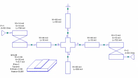
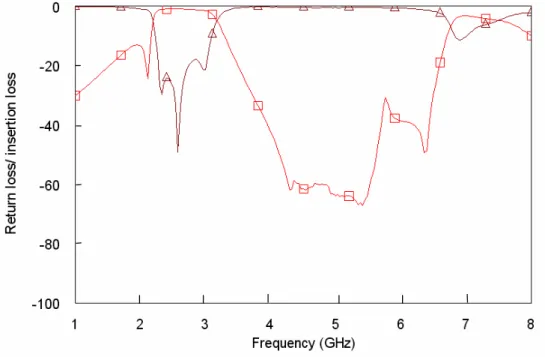
Fig. 2-10 and Fig. 2-11 are the simulated circuit schematic and result in AWR(circuit simulation) where Fig. 2-12 and Fig. 2-13 are the simulated physical layout and result in Sonnet(EM simulation). One thing needs to be noticed is that we bend the coupled line stage to reduce the area of the circuit. We adjust length of the coupled line at the same time. The simulated result of the bended …lter still shows good agreement with the original one, and we expect the measurement result will coincide with the simulaton result as well. A photograph of the fabricated …lter is given in Fig. 14. Fig. 2-15 and Fig. 2-16 plot measured performance in narrow band(1GHz 5GHz) and wide band(1GHz 8GHz), respectively. We can foresee that the spurious frequency will occur at three times above the center frequency.
Figure 2-10: Simulated schematic circuit of tri-mode …lter with an upper-stopband trans-mission zero in AWR
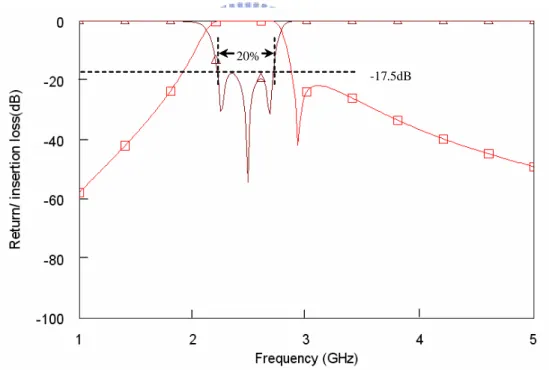
-19.5dB
19.3%
Figure 2-11: Simulated frequency response of tri-mode …lter with an upper-stopband transmission zero in AWR
Figure 2-12: Simulated physical layout of tri-mode …lter with an upper-stopband trans-mission zero in Sonnet
20%
-17.5dB
Figure 2-13: Simulated frequency response of tri-mode …lter with an upper-stopband transmission zero in Sonnet
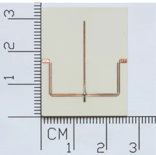
Figure 2-14: Photograph of tri-mode …lter with an upper-stopband transmission zero
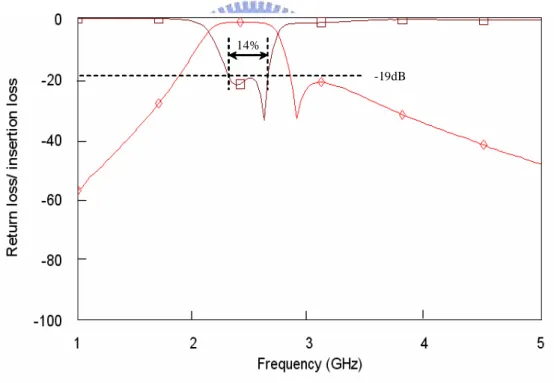
14%
-19dB
Figure 2-15: Measured frequency response of tri-mode …lter with an upper-stopband transmission zero(narrow band)
Figure 2-16: Measured frequency response of tri-mode …lter with an upper-stopband transmission zero(wide band)
The measured data shows that the in-band insertion loss is 1.43dB and the return loss is 19dB. Comparing to the simulation, the response with slightly shrunk bandwidth =14% agree with the simulation reasonably. Spurious frequency locates near 7.35GHz as we foretold before. It convinces us that the structure and the design rules for multi-mode resonator function well. And then, we can try to move the transmission zero to the lower side of the pass-band, whereas the previous …lter has the transmission zero on the higher side. We will see the design of triple-mode resonator …lter with a lower-stopband transmission zero in the next subsection, and validate with the experiment.
2.3.2
Tri-mode Resonator Filter with Lower-Stopband
Trans-mission Zero
Based on experience of the triple-mode resonator …lters in previous section, we suggest that triple-mode resonator …lters with a lower-stopband transmission zero can also be
synthesized easily. As we predicted before, the negative reactance leads to that z/4
microstrip line is going to be electrically longer than any of the resonators. It must be emphasized that the length of the open-circuit stub must be longer than the previous design. The relations between resonators are depicted in Fig. 2-17 and Fig. 2-18, and Fig. 2-19. Apparently, there is a transmission zero in the lower stop-band. A shunt capacitive reactance is used to represent –jX here. We try both lumped and distributed capacitor in this section.
-jX
2
1 3
λc/4 λc/4
λz/4
-jX -jX
1 2 3
-jX λz/4
λc/4 λc/4
Figure 2-18: Three resonators of tri-mode resonator …lter with negative jX
λz/4
2
Open
Short
Follow the same procedure, we must …nd out the key parameters of the triple-mode
resonator …lters with a lower stopband transmission zero. We will have c/4 and z/4
correspond to the speci…ed center frequency and zero frequency, respectively. Simulation with loose external coupling is depicted in Fig. 2-20. To simplify the simulation, we …x
impedance of c/4 transmission lines to be 50 which matches the port impedance of
the system. Then, the parameters Zopen(impedance of open-circuit stub) and C are left
to be designed. Fig. 2-21 and Fig. 2-22 indicate the parameters correspond to resonant frequencies- f1, f0, and f2 ,which are named by frequencies from low to high. We extract
the information from the comparison. First, f0 keep still at center frequency of 2.45
GHz despite of the changing in Zopen and C. It seems that f0 is principally decided by
two c/4 microstrip line. In addition, fz is controlled by the z/4 open-circuit stub and
located exactly where we designated. Zopen a¤ects f1 and f2 at the same time while C
have more in‡uences on f2 and less on f1.
C Zopen θopen=90°@ω=ωz Z0 θc=90°@ω=ωc Z0 θc=90°@ω=ωc
open Z =20Ω open Z =50Ω open Z =80Ω
Figure 2-21: E¤ect of the impedance of open-circuit stub(Zopen) on resonant frequencies
C=5pF C=15pF C=25pF
We collect these useful informations. Once the center frequency and bandwidth is
given, we can compute corresponding Chebyshev pole frequencies. We lay two c/4
microstrip lines in the middle to …x the f0. Next, we set the transmission zero frequency by changing the length of open-circuit stub. Then, Zopenmust to be decided before others,
because C in‡uences f1 less. In other word, we match the f1 to the pole of Chebyshev
response …rst. Afterwards, we change C for tuning f2 to meet the pole frequency. To
this step, the …lter design is fundamentally achieved. But we still need to add coupled lines at input/output stage to transform the above response to a Chebyshev band-pass response.
Both simulation and measurement of the 2.45 GHz multiple-mode resonator …lter with
bandwidth =20% are presented as follows. We calculate the corresponding resonant
frequencies by the Eqs. 2.3, 2.4, and 2.5, and then we have Chebyshev pole frequencies at
f1=2.18GHz, f0=2.45GHz, and f2=2.62GHz separately. Next step is to match the pole
frequencies. Since the center resonant frequency has been set by two c/4 microstrip
lines in the middle. We only need to tune Zopen to match f1 of the circuit to 2.18GHz,
and then adjust C to match f2 of the circuit to 2.62GHz.
Fig. 2-23 and Fig. 2-24 are the simulated schematic circuit and results in AWR(circuit simulation). Since lumped capacitor cannot be simulated in EM simulator, we fabricate the …lter directly without EM simulation. One thing needs to be noticed is that we bend the coupled line stage to reduce the area of the circuit. We adjust length of the coupled line at the same time to make sure the performance unchanged. Fig. 2-25 depict the photogragh of the circuit. Fig. 2-26 and Fig. 2-27 plot measured performance in narrow band(1GHz 5GHz) and in wide band(1GHz 8GHz). We can foresee that the spurious frequency will occur at three times above the center frequency.
Figure 2-23: Simulated schematic circuit of tri-mode …lter with strong coupling with a lower-stopband transmission zero in AWR
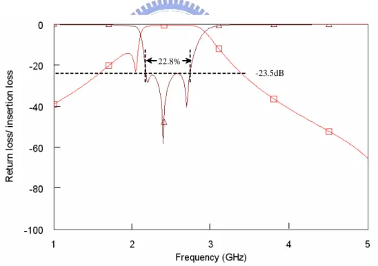
22.8%
-23.5dB
Figure 2-24: Simulated frequency response of tri-mode …lter with a lower-stopband trans-mission zero in AWR
Figure 2-25: Photograph of the tri-mode …lter with a lower-stopband transmission zero using a lumped capacitor
30.8%
-19dB
Figure 2-26: Measured frequency response of tri-mode …lter with a lower-stopband trans-mission zero using a lumped capacitor (narrow band)
Figure 2-27: Measured frequency response of tri-mode …lter with a lower-stopband trans-mission zero using a lumped capacitor(wide band)
The measured data shows that the in-band insertion loss is 0.9dB and the return loss is 19dB.When we implement the …lter at high frequency with lumped capacitor, there is a problem about value change of the capacitance. As we can see from the above …gures,
the measured bandwidth =30.8% is much larger than simulated one =22.8%. The
variation of the capacitance is unpredictable. We have to try several capacitors of di¤erent values to approximate the simulated performance. The capacitor chosen …nally is 1.8PF rather than 4.8PF used in simulation. The reason of the capacitance value drift is mainly due to the parasitic inductance of the chip capacitor. Because the equivalent circuit of this chip capacitor is unknown, the value change is unpedictable. The bandwidth of the …lter varies with the parasitic inductance.
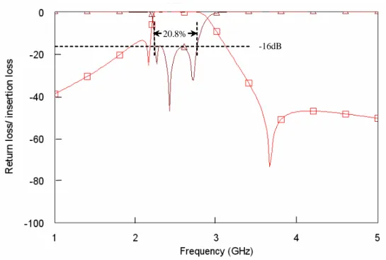
To eliminate the problem, we bring up the idea to replace lumped capacitor with distributed capacitor(patch capacitor). The physical layout and simulated result in Son-net have presented in Fig. 2-28 and Fig. 2-29. A photograph of the fabricated …lter is given in Fig. 2-30. We also depicted the measured data in Fig. 2-31 for narrow band(1GHz 5GHz) and Fig. 2-32 for wide band(1GHz 8GHz). Evidently, the mea-sured and the simulated performance matches much better than the previous one. This is a good information for the designer, since the characteristic of the circuit can be well-described.
Figure 2-28: Simulated physical layout of tri-mode …lter with a lower-stopband trans-mission zero using a patch capacitor in Sonnet
20.8%
-16dB
Figure 2-29: Simulated frequency response of tri-mode …lter with a lower-stopband trans-mission zero using a patch capacitor in Sonnet
Figure 2-30: Photograph of the tri-mode …lter with a lower-stopband transmission zero using a patch capacitor
20.7%
-21.5dB
Figure 2-31: Measured frequency response of tri-mode …lter with a lower-stopband trans-mission zero using a patch capacitor(narrow band)
Figure 2-32: Measured frequency response of tri-mode …lter with a lower-stopband trans-mission zero using a patch capacitor(wide band)
The measured data shows that the in-band insertion loss is 0.9dB and the return loss
is 21.5dB. The measured bandwidth =20.7% is almost consistent with the simulated
one =20.8%. The experiment veri…es that the capacitor implemented by distributed
element is more reliable than the one implemented by lumped element, especially in high frequency band.
2.3.3
Comparison of the Filter with Upper-Stopband
sion Zero and the Filter with Lower-Stopband
Transmis-sion Zero
There is an interesting topic here. The rejection ability of the …lter with upper-stopband transmission zero and the …lter with lower-stopband transmission zero at frequency near dc are quite di¤erent. This is reasonable because the tri-mode …lter with an upper-stopband transmission zero is naturally a third order …lter at low frequency. Two coupled line stages together with small short-circuit stub in the middle of c/2 microstrip line re-ject low frequency signal signi…cantly. However, the tri-mode …lter with a lower-stopband transmission zero only has two coupled line stages to suppress low frequency signal, which can be considered a two order …lter at low frequency. We can easily verify our prediction by demonstrate the contract between Fig. 2-33 and Fig. 2-34. Obviously, the insertion loss of the …lter with an upper stopband transmission zero near dc is approaching 100dB, while the insertion loss of the …lter with a lower stopband transmission zero near dc is approaching 60dB. In conclusion, the excellent low rejection ability of the low frequency signal is an attractive advantage of the proposed tri-mode …lter with an upper stopband transmission zero.
Figure 2-33: Low stop-band rejection ability of the tri-mode …lter with an upper-stopband transmission zero
Figure 2-34: Low stop-band rejection ability of the tri-mode …lter with a lower-stopband transmission zero
Chapter 3
J and K Inverter Filters
3.1
Filters with Ideal J and K inverters
3.1.1
Low-pass Prototype Filter
The element value g0, g1, g2,. . . , gn, gn+1 of th low-pass prototype …lters discussed in this chapter are de…ned as shown in Fig. 3-1(a) or (b). Either form has identical responses. The following conversions in Fig. 3-2 are observed:
G0=g0 L1=g1 Rn+1=gn+1 C2=g2 Cn=gn L3=g3 R0=g0 C1=g1 C3=g3 L2=g2 Ln=gn Rn+1=gn+1 (a) (b)
k k=1~n 0 1 1 0 0 1 1 n+1 n n n+1
the inductance of a series coil
g =
the capacitance of a shunt capacitor the generator resistance R if g =C g =
the generator conductance G if g =L the load resistance R if g =C g = th n+1 n n e load conductance G if g =L Figure 3-2: De…nition of gk
The circuit element values, gk, can be looked up in the tables with given speci…cation(pass-band ripple level and …lter order n). Fig. 3-3 is the table for the gkof Chebyshev reponse with pass-band ripple level =0.01dB and …lter order from 1 to 10.
As we mentioned before, J and K inverters can convert the …lter to all series or all shunt elements. Fig. 3-1 is the example of using K inverter to change shunt capacitors in Fig. 3-4 to series inductors, that is, we change the network to all series elements.
K01 K12 g0 g1 K23 g2 Knn+1 gn+1
Figure 3-4: Using K inverter to change shunt capacitors to series inductors
3.1.2
Low-pass Prototype Filter to Band-pass Filter
Transfor-mation
The low-pass prototype …lter in the previous section can be transformed to band-pass …lter through frequency transformation as shown in Eq. 3.1.
c
= 1(!
!0 !0
! ) (3.1)
where !0=2 f0 (f0 is the center frequency of the pass-band), =(!2!0!1)( is the
frac-tional bandwidth of the band-pass …lter), and c=1 ( c is the cuto¤ frequency of the
low-pass prototype …lter). Then, we have
jXk= j c gk = j 1 (! !0 !0 ! ) gk = j!Lk+ 1 j!Ck (3.2) where Lk=( gk!0), Ck =(!0 g k), and xk= !0 2 dXk
d! j!=!0 = !0Lk(xk is the reactance slope parameter of the resonator k). The band-pass after transformation is depicted in Fig. 3-5.
K01 K12
Rs K23 Knn+1 RL
L1 C1 L2 C2
Figure 3-5: Transform LPF to BPF
We can also obtain the equations as follows:
K01= s x0Rs g0g1 (3.3) Knn+1= s xnRL gngn+1 (3.4) Kkk+1 = rx kxk+1 gkgk+1 ; k = 1; 2; ::::; n 1 (3.5)
where Rs is the source resistance and RL is the load resistance. Follow the same rules,
we can also write the equations for J inverter.
J01 = s b1Gs g0g1 (3.6) Jnn+1 = s bnGL gngn+1 (3.7) Jkk+1 = s bkbk+1 gkgk+1 ; k = 1; 2; ::::; n 1 (3.8)
where Gsis the source admittance and GLis the load admittance. Follow the same rules,
3.2
Symmetric J and K Inverter Filters
As we mentioned before, J and K inverters can convert the …lter to all series or all shunt elements. It can be seen as a quarter-wavelength transformer. A quarter-wavelength
transformer can only contribute 90 delay at center frequency, while J and K inverter
can have +90 or 90 delays. And the delays providing by J and K inverters are
invariant over the whole spectrum. Evidently, the J and K inverters do not exist in real world. As a result, we usually …nd equivalent circuit around the center frequency of the band-pass …lter. Also, it is hard to implement wide bandwidth BPFs by using J or K inverters. However, it is a good design method for narrow to moderate bandwidth …lters. We can …nd equivalent networks for J and K inverters by letting ABCD matrices equal at the certain frequency. Fig. 3-7 and Fig. 3-8 are the examples for K and J inverters implementation, respectively. Inverters of this kind are suitable in transmission
lines …lter, because the /2 transmission lines with characteristic impedance Z0 can be
embedded into transmission line resonators.
K
+ 90°
J
+ 90°
ψ=negative Zo X=positive Zo (a) ψ=positive Zo X=negative Zo (b)
Figure 3-7: K inverters implementation with equal impedance transmission lines besides the shunt reactance
Zo Zo ψ/2 ψ=positive ψ/2 B=negative Zo Zo ψ/2 ψ=negative ψ/2 B=positive (a) (b)
Figure 3-8: J inverters implementation with equal impedance transmission lines besides the series susceptance
We can match Fig. 3-7 to K inverter and Fig. 3-8 to J inverter by equalizing the ABCD matrices. The ABCD matrix of K inverter and J inverter are
0 @ A B C D 1 A = 0 @ 0 jK jK1 0 1 A ; f(+)when + 90( )when 90 (3.9) 0 @ A B C D 1 A = 0 @ 0 j 1 J jJ 0 1 A ; f(+)when + 90( )when 90 (3.10)
The ABCD matrix of Fig. 3-7 and Fig. 3-8 are 0 @ A B C D 1 A = 0 @ cos 2 j sin(2) Y0 jY0sin 2 cos 2 1 A 0 @ 1 j 1 B 0 1 1 A 0 @ cos 2 j sin(2) Y0 jY0sin 2 cos 2 1 A (3.11) 0 @ A B C D 1 A = 0 @ cos 2 j sin(2) Y0 jY0sin 2 cos 2 1 A 0 @ 1 j 1 B 0 1 1 A 0 @ cos 2 j sin(2) Y0 jY0sin 2 cos 2 1 A (3.12)
We can have the following equations derived from ABCD matrices. Eq. 3.13 , Eq. 3.14 ,and Eq. 3.15 are the representation of K inverter,
K = Z0tan 2 (3.13) = arctan2X Z0 (3.14) X Z0 = K Z0 1 ZK 0 2 (3.15)
while Eq. 3.16 , Eq. 3.17 ,and Eq. 3.18 are the representation for J inverter.
J = Y0tan 2 (3.16) = arctan2B Y0 (3.17) B Y0 = J Y0 1 YJ 0 2 (3.18)
When we concentrate on the equations of K inverter, it is observed that X and /2 will have opposite polarities. Because the characteristic impedances on the both side of
X are equal so that above equations are quite simple. However, we will have some kind
of constraints on …lter design. To loose the constraints, the characteristic impedances on the both side of X are not necessary to be equal. The same analysis can be applied to J inverter. Next section will show the details of the asymmetric J and K inverter …lters.
3.3
Asymmetric J and K Inverter Filters
We have introduced how to use equal impedance transmission lines with a lumped circuit shunt reactance or series suceptance in between to realize J and K inverter …lters. Now, we want to use di¤erent impedance transmission lines instead. Naturally, the lengths of the transmission lines are varying with the impedances in the meanwhile. We can still write out the ABCD matrices and obtain relative equations by means of equalizing.
Z1 X=positive Z2 (a) X=negative Z2 (b) ψ1 ψ2 ψ1 ψ2 Z1 ψ1 ,ψ2 =negative ψ1 ,ψ2 =positive
Figure 3-9: K inverters implementation with unequal impedance transmission lines be-sides the shunt reactance
Zo Zo ψ2 ψ1,ψ2=positive ψ1 B=negative Zo Zo ψ2 ψ1,ψ2=negative ψ1 B=positive (a) (b)
Figure 3-10: J inverters implementation with unequal impedance transmission lines be-sides the series susceptance
We can match Fig. 3-9 to K inverter and Fig. 3-10 to J inverter by equalizing the ABCD matrices. The ABCD matrix of K inverter and J inverter are the same as the previous section. 0 @ A B C D 1 A = 0 @ 0 jK jK1 0 1 A ; f(+)when + 90 ( )when 90 (3.19) 0 @ A B C D 1 A = 0 @ 0 j 1 J jJ 0 1 A ; f(+)when + 90( )when 90 (3.20)
The ABCD matrix of Fig. 3-9 and Fig. 3-8 are
0 @ A B C D 1 A = 0 @ cos ( 1) jZ1sin ( 1) j sin( 1) Z1 cos ( 1) 1 A 0 @ 1 0 j 1 X 1 1 A 0 @ cos ( 2) jZ2sin ( 2) j sin( 2) Z2 cos ( 2) 1 A (3.21) 0 @ A B C D 1 A = 0 @ cos ( 1) j sin( 1) Y1 jY1sin ( 1) cos ( 1) 1 A 0 @ 1 j 1 B 0 1 1 A 0 @ cos ( 2) j sin( 2) Y2 jY2sin ( 2) cos ( 2) 1 A (3.22)
We can have the following equations by equalizing ABCD matrices. Absolutely, the computation is more complicated than the case discussed in the last section. However,
the degree of freedom increases. We can have various combinations of Z1 and Z2. Still,
we can have the equations as follows from the matrices. Eq. 3.23 , Eq. 3.24 ,and Eq. 3.25 are the representation of K inverter,
sin( 1 2) = K K2 Z 1Z2 (Z1 Z2) (3.23) sin( 1+ 2) = K K2+ Z 1Z2 (Z1+ Z2) (3.24) X = Z1Z2 Z1+ Z2 tan( 1+ 2) (3.25)
Simultaneously, Eq. 3.26 , Eq. 3.27 ,and Eq. 3.28 are the representation for J inverter.
sin( 1 2) = J K2 Y 1Y2 (Y1 Y2) (3.26) sin( 1+ 2) = J J2 + Y 1Y2 (Y1+ Y2) (3.27) B = Y1Y2 Y1+ Y2 tan( 1+ 2) (3.28)
To this end, we can decide the characteristic impedance Z1 and Z2 to have relative
1, 2, and X of K inverter. Besides, we want to use an open-circuit stub to implement X. X is positive(inductive) for l> c/4(quarter wavelength of the center frequency), and
negative(conductive) for l< c/4. Note that X will have opposite polarities of 1 and
2.We have known that the impedance of the open-circuit stub can be expressed as
which means
Zopen =jX tan lj (3.30)
where Zopen and l are the characteristic impedance and the length of the open-circuit
stub. However, the length of the open-circuit stub will decide the transmission zero frequency. The relation is shown as
open= l =
f0 fz
90 (3.31)
where f0 is the center frequency and fz is the transmission zero frequency. To conclude, we will obtain the value of 1, 2, and Zopen with given Z1, Z2, and z (wavelength of the transmission zero frequency). Our design is focused on the K inverter, but the procedure of designing J inverter is almost the same.
Based on the considerations given above, a third-order …lter, as shown in Fig. 3-11,
can be designed. However, the coupled line stage with a small additional degree 1 is
not easy for tuning. As a result, we rearrange the network in Fig. 3-11 a little to the one
in Fig. 3-12. We shorten the length of the coupled line to be a …xed degree c, but keep
the length of the …rst and last resonators to be 90 + 1.
1 90 +° φ 90 +° φ2 90 +° φ2 90 +° φ1 open θ θopen 1 Z Z2 Z2 Z1 open Z Zopen
J01
K12
K12
J01
2 90 +° φ 90 +° φ2 θc open θ θopen 1 Z Z2 Z2 Z1 open Z Zopen
J01
K12
K12
J01
c θ 1 90 +° φ 90 +° φ1Figure 3-12: Alternative network of third order …lter with proposed K inverter
From Eq. 3.6 and Eq. 3.5 in section 3.1.2 , we can obtain that
J01= s bquarterY0 g0g1 (3.32) K12= rx quarterxhalf g1g2 (3.33) where xquarter = Z41, xquarter = 2Z2, and bquarter = 4Z1 . Also, we can compute Zoo and
Zoe according to the Eq. 3.34 and Eq. 3.35.
Zoo01 = Z0 1 J01Z0csc ( c) + (J01Z0) 2 = 1 (J 01Z0cot( c))2 (3.34) Zoe01 = Z0 1 + J01Z0csc ( c) + (J01Z0) 2 = 1 (J 01Z0cot( c))2 (3.35)
In the end, we are well equipped for designing. The simulations and measurements of a K inverter …lter with an upper stopband transmission zero and K-inverer …lter with a lower stopband transmission zero will be presented in next two subsections.
3.3.1
K Inverter Filter with Upper-Stopband Transmission Zero
Firstly, we have to decide the characteristic impedances of the microstrip lines on the
either side of the reactance implemented by an open-circuit stub. Then, the value of J01
and K12 can be obtained on the basis of the Eq. 3.32 and 3.33 in the previous section.
We set Z1 to be 50 , which matches the port impedance of the system. We can have
relative 1, 2, and X from Eq. 3.23 , Eq. 3.24 ,and Eq. 3.25 by arranging Z2. Next, we
choose the frequency of the transmission zero fz to be located in the upper stop-band.
open and Zopen will be settle down at the same time. The list of the Zopen, 1,and 2
varying with the Z2 are shown as below. Fig. 3-14 also depicts the relations between Z2
and Zopen. The open-circuit stub is regarded as a capacitor when open < 90 . It means the reactance is negative, which results in 1 and 2 to be positive degree. The list also shows the good agreement with our supposition. And we will expect a transmission zero occurring at higher stop-band.
3.21 5.15 38.68 80 3.56 4.65 34.95 65 4.06 4.06 30.56 50 4.86 3.39 25.57 35 6.45 2.56 19.37 20 ψ2(° ) ψ1(° ) Zopen(Ω) Z2(Ω) fz=2.464GHz,θopen=83° 3.21 5.15 38.68 80 3.56 4.65 34.95 65 4.06 4.06 30.56 50 4.86 3.39 25.57 35 6.45 2.56 19.37 20 ψ2(° ) ψ1(° ) Zopen(Ω) Z2(Ω) fz=2.464GHz,θopen=83°
10 20 30 40 20 30 40 50 60 70 80 Z2(O) Z ope n(O )
Figure 3-14: Variation of Zopen with Z2 at fz= 2.464GHz
Now, we have the Z1, Z2, Zopen, open, 1, and 2, the rest are the Zoo01, Zoe01 which can be decided according to Eq. 3.34 and Eq. 3.35. Thus, all the parameters are ascertained. Next step is to fabricate a …lter to validate our design method. We aim at
the …lter with bandwidth =5% and passband ripple=0.01dB. Fig. 3-15 and Fig. 3-16
are the simulated scheme and frequency response in AWR. Further, simulated scheme and frequency response in Sonnet are illustrated in Fig. 3-17 and Fig. 3-18.
Figure 3-15: Simulated schematic circuit of third-order K inverter …lter with an upper-stopband transmission zero in AWR
5.8%
-17dB
Figure 3-16: Simulated frequency response of third-order K inverter …lter with an upper-stopband transmission zero in AWR
Figure 3-17: Simulated physical layout of third-order K inverter …lter with an upper-stopband transmission zero in Sonnet
5.5%
-19dB
Figure 3-18: Simulated frequency response of third-order K inverter …lter with an upper-stopband transmission zero in Sonnet
Finally, the photograph of …lter with asymmetric K inverter is shown in Fig. 3-19 and the experimental result is depicted in Fig. 3-20. The measured data shows that the in-band return insertion loss is 1.7dB and the return loss is 16.5dB. Comparing to
the simulation, the response has slightly extended bandwidth =6.2%. We validate the
Figure 3-19: Photograph of third-order K inverter …lter with an upper-stopband trans-mission zero
6.2%
-16.5dB
Figure 3-20: Measured frequency response of third-order K inverter …lter with an upper-stopband transmission zero
3.3.2
K Inverter Filter with Lower-Stopband Transmission Zero
Tracing the same procedure of designing K inverter …lter with lower stopband transmis-sion zero, we have to decide the characteristic impedances of the microstrip lines on the either side of the reactance implemented by an open-circuit stub. Then, the value of
J01 and K12 can be obtained on the basis of the Eq. 3.32 and 3.33 . We set Z1 to be
50 , which matches the port impedance. We can have relative 1, 2, and X from Eq.
3.23 , Eq. 3.24 ,and Eq. 3.25 by arranging Z2. Next, we choose the frequency of the
transmission zero fz to be located in the lower stop-band. open and Zopen will be settle down in the meanwhile. The list of the Zopen, 1,and 2 varying with the Z2 are shown
as below. Fig. 3-22 also depicts the relations between Z2 and Zopen. The open-circuit
stub is regarded as a inductor when open > 90 . It means the reactance is positive,
which results in 1 and 2 to be negative degree. The list also shows the good agreement with our supposition. And we will expect a transmission zero occurring in the lower stop-band. -3.21 -5.15 32.89 80 -3.56 -4.65 29.64 65 -4.06 -4.06 25.99 50 -4.86 -3.39 21.75 35 -6.45 -2.56 16.47 20 ψ2(° ) ψ1(° ) Zopen(Ω) Z2(Ω) fz=2.254GHz,θopen=98° -3.21 -5.15 32.89 80 -3.56 -4.65 29.64 65 -4.06 -4.06 25.99 50 -4.86 -3.39 21.75 35 -6.45 -2.56 16.47 20 ψ2(° ) ψ1(° ) Zopen(Ω) Z2(Ω) fz=2.254GHz,θopen=98°
10 20 30 40 20 30 40 50 60 70 80 Z2(O) Z ope n (O )
Figure 3-22: Variation of Zopen with Z2 at fz= 2.254GHz
Now, we have the Z1, Z2, Zopen, open, 1,and 2, the rest are the Zoo01, Zoe01 which can decided according to Eq. 3.34 and Eq. 3.35. Thus, all the parameters are ascertained. Next step is to fabricate a …lter to validate our design method. We target at the …lter
with bandwidth =5% and passband ripple=0.01dB. Fig. 3-23 and Fig. 3-24 are the
simulated schematic circuit and frequency response in AWR.
Figure 3-23: Simulated schematic circuit of third-order K inverter …lter with a lower-stopband transmission zero in AWR
4.4%
-19.5dB
Figure 3-24: Simulated frequency response of third-order K inverter …lter with a lower-stopband transmission zero in AWR
Although Zopen raise along with Z2, we …nd that Zopen is still too small. This will make the linewidth of the open-circuit stub too wide to implement. We need to do some adjustment about the layout. We suggest that a single open-circuit stub with the characteristic impedance Zopencan be transformed to two parallel open-circuit stubs with
characteristic impedance 2Zopen. In addition, we add the transitions to where the
open-circuit stubs taper in, and we revise the length of the stubs. The layout after changes is exhibited as Fig. 3-25, which is the simulated scheme in Sonnet. The result of the simulation in Sonnet is presented in Fig. 3-26 as well.
Figure 3-25: Simulated physical layout of third-order K inverter …lter with a lower-stopband transmission zero in Sonnet
6%
-19.5dB
Figure 3-26: Simulated frequency response of third-order K inverter …lter with a lower-stopband transmission zero in Sonnet
At last the photograph of the …lter with asymmetric K inverter and lower stopband transmision zero is displayed in Fig. 3-27. And the experimental result is depicted in Fig. 3-28. The measured data shows that the in-band return insertion loss is 1.7dB and the return loss is 23dB. Comparing to the simulation, the response has slightly shrunk
bandwidth =5.5%. Hence it can be concluded that the designing method in this chapter
can be applied on both the K inverter …lter with an upper stopband transmission zero and the K inverter …lter with a lower stopband transmission zero.
Figure 3-27: Photograph of third-order K inverter …lter with a lower-stopband transmis-sion zero
5.5%
-23dB
Figure 3-28: Measured frequency response of third-order K inverter …lter with a lower-stopband transmission zero
Chapter 4
Conclusion
In Chapter 2, we submit a novel structure for multiple-mode resonator …lters. Both of the tri-mode …lter with an upper-stopband tranmission zero and the tri-mode …lter with a lower-stopband tranmission zero have been synthesized and implemented by multi-mode resonator method. The resonant frequencies of the proposed multiple-multi-mode have been allocate to match the transmission poles of the of a Chebyshev pass-band. It has been validated that a con…gurable transmission zero can be decided by an open-circuit stub with a small short-open-circuit stub or a capacitor in parallel. The simulations and measurements of the tri-mode …lters with center frequency 2.45GHz and fractional
bandwidth =20% are presented. The measured frequency responses match well with
the simulated ones. Despite the advantages such as compact size, systematic design procedure, and high selectivity, the proposed tri-mode resonator …lters can push the transmission zero frequency to three times higher than the center frequency. Furthermore, the triple-mode …lter with a upper-stopband tranmission zero has one more desirable property- excellent rejection ability for low frequency signal.
In Chapter 3, a completely di¤erent method of synthesizing …lters has been intro-duced. We fabricated the …lters with K inverter which are formed by two di¤erent im-pedances and lengths microstrip lines with centered open-circuit stub. All the required parameters can be determined by equalizing the ABCD matrices. If the stub is shorter
than the quarter wavelength of center frequency, it can be seen as a negative reactance resulting an upper stopband transmission zero. On the other hand, the stub longer than the quarter wavelength of center frequency will lead to a lower-stopband transmission zero. The experiments of making the third order …lters with center frequency 2.45GHz
and fractional bandwidth =5% indicate the method is more ‡exible than the
conven-tional design.
Although both methods of …lter design can achieve third order …lter with tunable transmission zero, the former has more elegant properties such as smaller size, wider pass-band range, wider upper stop-band range, and higher out-of-band rejection ratio. Accordingly, the multimode resonator …lters are more attractive to commercial applica-tions.
Bibliography
[1] David M. Pozar, Microwave Engineering, 3rd ed. New York:Wiley, 2005.
[2] L. Zhu, H. Bu, and K. Wu, “Aperture compensation technique for innovative design of ultra-broadband microstrip bandpass …lter,” in IEEE MTT-S Int. Dig., pp.315-318, Jun. 2000.
[3] W. Menzel, L. Zhu, and K. Wu, “On the design of novel compact broad-band planar …lters,” in IEEE Tran. Microw. Theory Tech, vol. 51, no. 2, pp.364-370, Feb. 2003. [4] L. Zhu, S. Sun, and W. Menzel, “Ultra-wideband (UWB) bandpass …lters using multiple-mode resonator,” in IEEE Microw. Wireless Compon. Lett., vol. 15, no. 11, pp.796-798, Nov. 2005.
[5] L. Zhu and H.Wang, “Ultra-wideband (UWB) bandpass …lter on aperture-backed microstrip line,” in Electron. Lett., vol. 41, no. 18, pp.1015-1016, Sep. 2005.
[6] L. Zhu, H.Wang, and W. Menzel, “Ultra-wideband (UWB) bandpass …lters with hybrid microstrip/CPW structure,” in IEEE Microw. Wireless Compon. Lett., vol. 15, no. 12, pp.844-846, Dec. 2005.
[7] Y.-C. Chiou and J.-T. Kuo, “Broadband quasi-Chebyshev bandpass …lters with mul-timode stepped-impedance resonators (SIRs),” IEEE Tran. Microw. Theory Tech, vol. 54, no. 8, pp.3352-3358, Aug. 2006.
[8] R. Li and L. Zhu, “Compact UWB Bandpass Filter Using Stub-Loaded Multiple-Mode Resonator,” in IEEE Microw. Wireless Compon. Lett., vol. 17,no. 1, pp.421-423 Jan. 2007.
[9] S.- W. Wong and L. Zhu, “EBG-Embedded Multiple-Mode Resonator for UWB Bandpass Filter With Improved Upper-Stopband Performance,” in IEEE Microw. Wireless Compon. Lett., vol. 17, no. 6, pp.40-42, Jun. 2007.
[10] M.-H. Ren, D. Chen, C.-H. Cheng, “A novel wideband bandpass …lter using a cross multiple-mode resonator,” in IEEE Microw. Wireless Compon. Lett., vol. 18, no. 1, pp.13-15, Jan. 2008.
[11] S.- W. Wong and L. Zhu, “Implementation of Compact UWB Bandpass Filter With a Notch-Band,” in IEEE Microw. Wireless Compon. Lett., vol. 18, no. 1, pp.10-12, Jan. 2008.
[12] G. L. Matthaei, L. Young, and E. M. T. Jones, Microwave Filters, Impedance-Matching Network, and Coupling Structures. Norwood, MA: Artech House, 1980. [13] J.-R. Lee, J.-H. Cho, and S.-W. Yun, “New Compact Bandpass Filter Using
Mi-crostrip /4 Resonators with Open Stub Inverter,” in IEEE Microw. and Guided