Nonlinear analysis and design of an active multiplier
antenna array
Shin-Der Yang and Tah-Hsiung Chu* Electrical Engineering Department, National Taiwan University
No.1, Sec. 4, Roosevelt Road, Taipei, Taiwan, R.O.C.
1. Introduction
Spatial and Quasi-optical power combining technique is a promising approach for overcoming the inherent power limitation of solid-state devices at the millimcter-wave fiequency range [I]. Such array can effectively cooperate with large numbers of devices. By combining their power in free space, it may achieve low combining loss and hence high combining efficiency. However, at millimeter and submillimeter wave frequency region solid-state devices have limited power performance with poor power added efficiency. In addition, there IS always a frequency limit at which a solid-state oscillator can operate. In that limit, the negative resistance produced by active device can not compensate the resonator loss.
One way to generate signal at such Frequency is to use the active device nonlinearity to yield with higher-order harmonics as a frequency multiplier. There are several methods to increase the output harmonic power. In [Zl, the multiplier is designed with optimized harmonic termination impedance for higher output power. In 131, a periodic load method is proposed by strongly coupling between devices. However, strongly coupled oscillator array must encounter with problems such as multi-mode of node voltages and symmetric arrangement of oscillators. In this paper, we develop an active multiplier array structure which consists of oscillators by directly matching at the second-harmonic frequency and considering the clipping effect within FET. Using fliis structure, the multiplier antenna array not only can yield with higher output harmonic Signal power but also has the benefit for scanning array application. The scanning angle under second harmonic operation is twice of that under fundamental operation [4].
11. Formulation
In the analysis, we firstly use the harmonic-balance method to solve the input impedance of individual oscillator and then apply the weakly coupled oscillator theory to
analyze the phase distribution of antenna array. Assume the following two conditions are satisfied. One is the free-running oscillation frequency and amplitude deviation between array elements are small. In addition, the change of voltage amplitude of individual element afler coupling is small [ 5 ] . One can then separate the amplitude and phase dynamic into individual differential equation. For the i-th oscillator, its voltage waveform at coupling tiode is represented as
V,(t)=Re[(A,, +~;(r))e1'2"1'*4~"''
1
(1) where A,,,
is the i-th oscillator free-running voltage amplitude at fundamental frequency.G(t)
IS the amplitude transient after inter-locking, and the reference frequency.f,
is theinjection source frequency or the average free-running frequency of entire oscillator array when no extern injected source presents. By only considering the weakly nonlinear oscillator operation, one can Writc the dynamic equalion ofphase and amplitude as
where
In (2) and (3), '+' sign is for parallel resonance oscillation, and '-' sign is used for series resonance oscillation. K and
y
are nonlinear parameters to he solved using the harmonic-halance method. From (2) and (3). one can see that phase o f each array element can be varied by tuning the free-running frequency ofeach oscillator in the array.111. Design and measurement A. Antenna element
Figure 1 is the schematic diagram of each active multiplier antenna element. It uses source feedback configuration with LI to give negative resistance at 4 GHz and L21+L22 =
Lg
/ 4 at 4 GHz. Thus, the input impedance at B for L21+L22 is an open at 4 GHz and a shon at 8 GHz The length of LZI is 7mnl and L22 is 4.7mm. From the node voltages that derived by initial design, we can vary the L22 length to match Zout and Zload at the second- harmonic frequency. Figure 2 shows Zout and Zload on the Smith chart for two different L22. One can see that L22=2.4mm has a better match than that in the initial design with L22=4.7mm. The simulation and measurement results of the output second-harmonic signal power level is 3 dBm for L 2 2 4 . 7 and 6 dSm for L22=2.4m. Furthermore, one can adjust the bias point to yield with a larger second-harmonic current. From Fig. 3, one can see that the bias point with Vgs-0.2V and Vds=3V has a better clipping current waveform for the second -harmonic frequency. At this bias point, the second-harmonic output is 9dBm from simulation, which is close to the measurement result of9.5dBnl
B. Multiplier antenna array
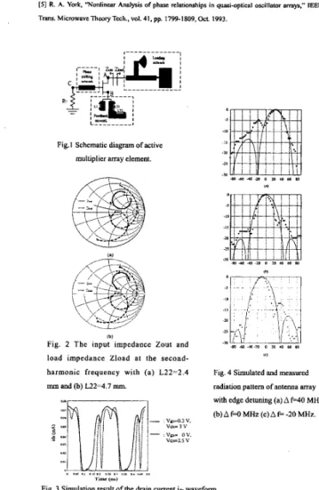
For the active multiplier antenna array design, we use the neighbor coupling architecture. Table 1 gives the array design parameters. From ( 2 ) , one call solve the fundamental and second-harmonic node voltage phase difference, and calculate the array radiation pattern after edge detuning. Table 2 gives the measured and simulated results of array EIRP, and Fig. 4 shows the measured and simulated array radiallon pattcm.
lgblu I Dcsign parameters of active rnulliplier antenna array
I I
I
17.4 &?mL22=4 7 nun, LI=9 I imn
L22=2.7 mm. LI=8.5 mm 121.5 dBm
I
22.68 dBmI19 dBm
Table 2 Measurement and simulation results of antenna array EIRP. Summary
Analysis of a coupled active multiplier antenna array ou its matching method for the second-harmonic output power is developed. By using the harmonic-balance method and weakly couple oscillator dynamic theory, one can well predict its second-harmonic output power. matching condition and phase distribution between array elements. Impedance matching using large-signal and small-signal analysis concept can increase the output power about 3dB. By further considering the clipping effect of bias condition, the output power can be increased about 6dB to be 9.5 dBm. The measurement results are shown in good agreement with simulation results.
References
[ I ] K. Chang and C. Sun, “Millimeter-wave power-combining techniques”. IEEE Trans. Microwave TheoryTech.,vol. 31 no. 2,pp. 91-107, Feb. 1983.
121 D. 0. Thomas, 11. and G. R. Branner, “Optimization of active microwave frequency multiplier performance utilizing harmonic terminating impedance,” IEEE Trans. Microwave Theory Tech., vol. 44, pp. 2617.2624, Dec 1996.
[3] A. Mortazawi, H. D. F o l k aud T. Itoh, “A periodic second harmonic spalial power combining arcillator”, IEEE Trans. Microwave Theory Tech., vol. 40, pp. 851-856, May 1992.
[4] A. Alexnian, H. C. Chang, and R. A. York, “Enhanced scanning range in coupled oscillator arrays
ulilinng frequency mulhpliers,” 1995 TEEE Antennas Pmpagation Symposium Dig. pp. 1308-1310, 1995.
151 R. A. York. ‘Wonlinear Analysis of phase relationships in quasi-optical oscillator arrays,’’ IEEE Trans. MicmwavcTharyTech.,vol.41,pp. 1799-1809,Oct. 1993.
Fig. I Schematic diagram of active multiplier array element.
lbl
Fig. 2 The input impedance Zout and load impedance Zload at the second- harmonic frequency with (a) L22=2.4 nun and (b) L22=4.7 mm.
m a 4 UI 0 20 ‘0 M IYI
,
m M 4 m ( I , O , O M l o
,
Fig 4 Sunulated and measured radauon pattern of antenna array with edge d e t u g (a) A
W O
MHz(b)Af=O MHz(c)Af=-20MHz
Fig. 3 Simulation result of the drain cnrtentia. waveform.