具高度差之晶圓在化學機械研磨中之研磨機制與研磨參數研究 計劃編號:NSC89-E-002-022 執行期間:八十八年八月一日至八十九年七月三十一日 主持人:陳達仁,國立台灣大學教授 計畫參與人員:李伯勳、張世昌、林宏舜 摘要 本研究計畫旨在建立化學機械研磨之晶圓研磨 模型,其中將考慮晶圓表面高度差對研磨的關係; 並研究研磨參數的變化對於研磨特性之影響。 文中所建立之化學機械研磨模型,將焦點放在研 磨的機械效應上。首先建立一個化學機械研磨之研 磨模型,考慮晶片表面高度差經由研磨而減少,進 而提出一個與時間相關的研磨速率公式。在研磨運 動的研究上,建立了一個開迴路操作器的模型。由 此等效模型,進而求得研磨速率的表示式;並將研 磨速率表現為化學機械研磨機之幾何外型、轉速比 及研磨墊轉速的函數。此外,配合實驗的資料,以 取得必要的研磨參數,建立完整的研磨模型。 利用研磨模型,可以求得研磨時間、研磨厚度及 平坦化效率的表示式。其中,研磨時間、研磨厚度 及平坦化效率,能夠顯示化學機械研磨在局部點的 研磨行為。另一方面,全面平坦化的均勻性和研磨 參數間的關係,也能夠求得。最後將提出這些研磨 參數變化的效果,以及所造成的影響,說明研磨參 數調整的方向。本計畫的結果,能提供一個有效的 預測和改善化學機械研磨製程。 ABSTRACT
A polishing model of chemical mechanical polishing (CMP) is established with consideration of the effects of pattern density. This paper fo-cuses on mechanical polishing behaviors and isolates the roles of chemical effects when pat-terns exist. A three-link manipulator, which is in equilibrium with the polishing motion of CMP, is adopted to study the kinematics of CMP. Time-dependent removal rate formulas are presented by considering the decrement of pattern step height. The necessary parameters wear coeffi-cient and loading density coefficoeffi-cient, are ob-tained by fitting to experimental data and the complete model is presented.
Based on the pattern planarization model, the polishing time, the polished thickness and the planarization efficiency of a point of interest on the wafer during chemical-mechanical process are expressed as function of polishing parame-ters. The influences as well as the variation of the polishing time, polished thickness and the pla-narization efficiency across the wafer are also presented. The polished thickness uniformity and the planarization uniformity are also presented. The effects of the polishing parameters on the process are discussed and the predicted trends in adjusting these polishing parameters are
illus-trated.
1. Introduction
Chemical mechanical polishing (CMP) is one of the most effective planarization technologies for achieving smaller feature size and multilevel interconnections for the integrated circuit (IC) industry. CMP is used for planing interlevel di-electrics (ILDs) and metal films in general and can be extended to many planarization tech-niques in device fabrication. Because of its ability to meet the increasingly stringent lithographic requirements of device manufacture on silicon wafer, CMP is receiving increasing attention in the fabrication of ULSI/VLSI chips.
The polishing mechanism, process control and basic understanding of CMP remain essentially on the experiential level. There is a variety of physical and chemical effects that are involved in the CMP process and analysis from various science and engineering fields are needed. It is assumed that the polishing mechanism is a func-tion of both chemical effects and mechanical effects. Chemical effects are achieved by apply-ing the slurry to the wafer and changapply-ing the chemical properties of the wafer. Chemical reac-tions between slurries and the wafer surface change the solubility and mechanical properties of the wafer surface. The mechanical process is affected by the down force, the rotational speeds of the pad and the wafer, the density and viscos-ity of the slurry, and the material and the surface microstructures of pad and carrier film. Most previous research has focused on planarization behavior in polishing blanket wafer. The Preston equation, an experiential equation for glass pol-ishing, summarized the mechanical removal rate and hence provided a way for process control. Cook (1990) reviewed the mechanics and chemical polish for glass polishing and proposed a micro-cutting mechanism to simulate the breaking of chemical bonds. Runels and Eyman (1994) analyzed the fluid film between wafer and pad. Based on statistical method and elastic theory, Liu et al. (1996) showed that the removal rate is dependent on the elastic modulus of the slurry particle and polished film. Tseng (1997) modified the Preston equation and showed the removal rate is proportional to the terms P5/6
and V1/2. However, the polishing of blanket wafer and patterned wafer is different. The element configu-ration on the wafer affects the results of CMP planarization and can behave in a different way.
In this model, the polishing motion is also studied based on the principle of kinematic inversion. Experimental results conduce to necessary parameters and the verification of the CMP model. This semi-experimental model allows quantitative evaluation of a given CMP process and provides a basis for process optimization to meet specific technological requirements for planarization.
2. Polishing Model
A schematic diagram of the CMP is shown in Fig. 1. The wafer is mounted upside down on the wafer carrier and rotated above a pad sitting on a table. The slurry that flows between the wafer and the pad dissolves and removes the wafer layer. Figure 2(a) shows a schematic cross-section of wafer surface. There are elements constructed on the wafer surface with different features and the pad is deflected by the down force. An initial step height, h0, between the up-per and lower feature surfaces is shown in Fig. 2(b). The polished thicknesses on upper and lower feature surfaces are denoted as δU and δL. For the upper feature surface area, AU, and the lower feature surface area, AL, we have:
L
U A
A
A= + (1)
where, A is the total wafer area.
The pattern density, D, can be defined as A
A
D= U (2)
In the following, polishing behavior with the existence of patterns is considered with the fol-lowing assumptions
A1. The material removal is anisotropic down-ward and has no effect on the sidewall of the profiles, i.e. PA A P A PU U+ L L = (3)
where PU and PL are the pressures on the upper and lower feature surfaces, and P is the total pressure.
A2. The pressures on the upper and lower sur-faces are directly proportional to the step height, h, i.e.
h P
PU− L =α (4)
where the loading density coefficient, α, indicates the stiffness of the polishing pad.
A3. The polishing mechanism of every point on the wafer follows the linear wear equation (Rigney, 1965)
H KLS
W= (5)
where W is the wear volume, K is the wear coefficient, L is the down force of the pad onto the wafer, S is the polishing path of the polished point and H is the hardness of the polished material.
From Eqs. (2), (3) and (4), PU and PL can be written as
(
1 D)
h P h A A P PU = + L α = + − α (6) and h D P h A A P PL= − Uα = − α (7)Since the wear volume is equal to the polished thickness, δ, times the polished area, Eq. (5) can be rewritten as S A L H K = δ (8)
By taking the derivative of Eq. (8), the removal rate can be written as
p V P H K S A L H K dt d = = δ& (9)
By substituting Eqs. (6) and (7) into Eq. (9), the removal rate of the upper and lower surfaces, δ&U and δ&L, can be written as
(
)
(
P 1 D h)
V H K p U= + − α δ& (10) and(
P D h)
V H K p L= − α δ& (11)Since the rate of decrease in step height is the difference of the removal rate between the upper and lower surfaces, we have
) ( dt dh L U−δ δ − = & & (12)
or by substituting Eqs. (10) and (11) into Eq. (12), 0 h V H K dt dh pα = + (13)
Equation (13) can be solved with initial step height h0 as − α = V t H K exp h h 0 p (14)
By substituting Eq. (14) into Eqs. (10) and (11), we have
(
)
− α α − + = δ V t H K exp h D 1 P V H K p 0 p U & (15) and − α α − = δ V t H K exp h D P V H K p 0 p L & (16)Equations (15) and (16) show the time-dependant removal rate on the upper and lower feature surfaces of the wafer. The variables in these equations are K, H, P, α and Vp. The pol-ishing velocity, Vp, can be adjusted by changing the angular velocity of the table and carrier. However, the polishing velocity is a time-dependent term and it differs from point to point. In the following section, the kinematics of CMP will be studied.
3. Kinematics of CMP
points Ot and Ow are the rotational centers of the polishing pad and the wafer, respectively. The distance between points Ot and Ow is a1, and points Ow and A is a2. For a referenced point ″A″ on the wafer which is coincident with a point ″B″ on the pad, the relative velocity of point B to A is defined as the polishing velocity at point A.
Accordingly, the geometry of the polisher shown in Fig. 3(a) can be expressed as a three-link open-loop arm as shown in Fig. 3(b). The coordinate systems can be established accord-ing to the D-H convention. The table rotataccord-ing with respect to ground is just link 0 with respect to link 1. The joint angle θ1 is the angle from link 1 to link 0. From the kinematic inversion, the angular velocity of the table, ωt, can be expressed by the derivation of joint angle θ&1 that is the same as ωt in magnitude but opposite in direction. That is
1 t = &−θ
ω (17)
and the angular velocity of wafer, ωw, can be written as
2 w= &θ
ω (18)
The angular velocity of each link and the linear velocity at the origin (xi, yi, zi) coordinate system can be derived from the forward recursive equa-tions as
(
i 1 i 1 ii, 1i 1 i 1)
1 i i i i R z − − − − − − +θ = ω & ω (19a) and i i i i 1 i 1 i 1 i i i i p v R v= − − − +ω× (19b) where iRi-1 is the rotation matrix from the i-th to the (i-1)-th coordinate system, i-1
zi-1 is [0, 0, 1] T
, and ip
i is the position vector defined from oi-1 to oi. (Martin, 1982)
For the kinematic model shown in Fig. 4, 1
p1 = [a1, 0, 0] T , 2 p2 = [a2, 0, 0] T and with 0 0 = 0 v0 = [0, 0, 0]T , we have θ θ − θ θ = − 1 0 0 0 cos sin 0 sin cos R i i i i 1 i i (20)
and from Eqs. (19a) and (19b), we have
[
]
T 1 1 1ù = 0 0 θ& (21a)[
]
T 2 1 2 2ù = 0 0 θ&+θ& (21b) = × + = 2 2 2 2 1 1 1 2 2 2 p ù V R V T 2 1 2 1 2 1 1 2 1sin ,a cos a ( ),0] a[ θ θ& θ θ&+ θ&+θ& (21c)
Let the angular velocity ratio, kv, be defined as the angular velocity ratio of wafer to pad, i.e,
1 2 v k θ θ − = && (22)
By rewriting Eq. (21c), the magnitude of the pol-ishing velocity can be written as
⋅ θ = 1 p V &
(
)
(
)
(
)
2 1 2 v 2 1 2 v 2 2 2 1 a k 1 2aa k 1cos a + − − − θ (23)From Eq. (23), the polishing velocity of a point varies with position. The values of a1, a2 and θ2 indicate the position of a considered point and only the variable θ2 is a function of time. It can be found that the polishing velocity will repeat for θ2 passing through an angle 2π. The period of pol-ishing velocity can be as θ2 goes from 0 to 2π. To obtain the average polishing velocity, the polish-ing path of a point durpolish-ing a period is needed. The polishing path, S, can be calculated by integrat-ing the polishintegrat-ing velocity in Eq. (23)
( )
m E k G 4 S v = (24) where( )
m =∫
π(
1−msin θ)
dθ E 02 2 12 (25a)(
)
2 v 2 1 G k 1 a a 4 m= − (25b) and 2 v 2 1 a k a a G= + − (25c)Equation (25a) is the complete elliptic integral, which has been tabulated and is readily available in most mathematical handbooks such as Peiroc (1961). From Eq. (24), the average polishing velocity can be obtained as
( )
m E G 2 k 2 S 2 S V 1 1 v 2 avg =π θ θ π = θ π= & & & (26)
By ignoring the small variation in polishing velocity, the average polishing velocity can be used instead of the polishing velocity. Substitut-ing Eq. (26) into Eqs. (15) and (16), we have
(
)
(
P 1 D h h) ( )
Em G H K 2 n 0 1 U= π θ + − α δ& & (27) and(
P D h h) ( )
Em G H K 2 n 0 1 L= π θ − α δ& & (28)where hn is the normalized step height and is defined as the ratio of step height to initial step height. That is:
( )
θ α π − = = GEm t H K 2 exp h h h 1 0 n & (29)From Eq. (27), the removal rate of the upper feature surface of the wafer will decay with time due to the decrease in step height. On the other hand, from Eq. (28), the removal rate of the lower feature surface will increase with time. When the step height is close to zero, the removal rate of upper and lower feature surfaces are similar to each other. The normalized step height, hn, in close proximity to zero indicates a good planari-zation effect. The initial state of normalized step
height is one. Hence, normalized step height, hn, can be used as a planarization index. To improve the throughput, the normalized step height has to decay faster. This can be achieved by adjusting the polishing parameters in these equations. 4. Model parameters
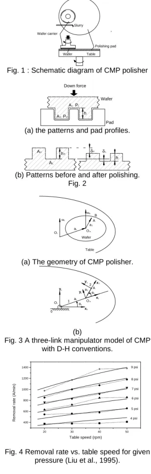
Two experiments are needed to acquire the necessary parameters, K and α, in the polishing model. The first experiment adopts the polishing of a blanket wafer to obtain the wear coefficient K while isolating the influences of the parameter α. In order to investigate the loading density α, the second experiment employs the polishing of a wafer with patterns on its surface with the reason that α only functions when there are step heights. 4.1 Parameter K
The wear coefficient K is associated with mate-rial properties, slurry concentration, and chemical processes during CMP. It can be assumed that the wear coefficient is a function of down pres-sure, table speed and the angular velocity ratio, i.e., j v n 1 m cP k K K= θ& (30)
The experimental data cited below are from Liu et al. (1996). The experimental conditions are a. a 6 inch blanket wafer with thermal silicon di-oxide film deposited on its surface.
b. carrier speed: 42 rpm. c. down pressure: 4-7 psi. d. table speed: 20-50 rpm. e. polishing time: 120 secs.
Thicknesses before and after polishing are measured at 0.6 cm intervals at 12 points along the right radius on a wafer. Then the average removal rate is obtained from the average value of polishing thickness obtained from these 12 points. The theoretical removal rate can be ob-tained by averaging the values at these 12 points. That is: V P H k P K V 12 1 H KP 12 1 12 c m 1n vj 1 i i p 12 1 i i θ = = δ
∑
∑
= = & & (31)where, V is the average polishing velocity at these 12 points.
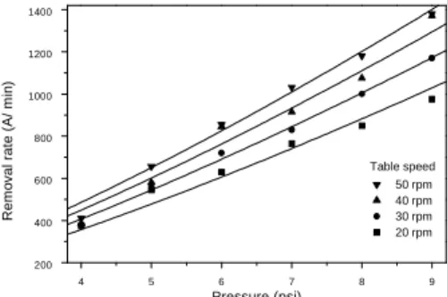
The average removal rate data are plotted against carrier speed in Fig. 4 for a variety of pressures. By assuming that the theoretical re-moval rate matches the experimental data, the method of least square fits can be used to obtain the values of Kc, m, n and j. The data are fitted to the model developed above with constant P. The value of Kc is 24.72, m is 0.30, n is –0.79 and j is -0.14. Figure 5 shows the relation of removal rate and pressure under a given table speed.
4.2 Parameter α
The loading density coefficient α is associated with the pad material properties. The pad is in compliance either with the upper or lower pattern
surfaces. The experimental conditions are a. Carrier speed: 42 rpm.
b. Table speed: 20 rpm. c. Down pressure: 7 psi.
d. BPSG covered patterns (the hardness relative to thermal dioxide is about 0.6).
The method of least square fits cab be used to obtain a value for α of 0.7974 TPa/m. Figure 6 shows the normalized step height decays with time.
5. Parameter analysis
5.1 Variation of Polishing Time
From Eq. (14), the polishing time can be ob-tained as
( )
hn ln ) KV ( H t α − = (32)From Eq. (32), it can be seen that the polishing time varies from point to point due to the posi-tion-dependent polishing velocity. Assuming the polishing conditions such as the pad condition, pad hardness, loading coefficient and wear coef-ficient across entire wafer remain stable, then from Eq. (32) the polishing time at wafer center, T0, can be written as
( )
n 0 0 lnh KV H T α − = (33)Let the polishing time for planarization on the wafer center point be T0. The polishing time with respect to T0 to reach the requirement of planari-zation can be obtained as
v
0 R
1 T
t = (34)
From Eqs. (12) and (13), it can be seen that the polishing time with respect to T0 is a function of the position ratio and the angular velocity ratio. Figure 7 shows the polishing time with respect to T0 versus the position ratio for polishing a TEOS film with applied pressure of 7 psi at various an-gular velocity ratios.
5.2 Variation of Polished Thickness
The polished thickness for planarization at upper feature surface, δU, and lower feature sur-face, δL, can be obtained by integrating Eqs. (15) and (16) as
( )
n 0(
)
[
n]
U lnh h 1 D 1 h P − − + α − = δ (35) and( )
n 0[
n]
L lnh h D1 h P − − α − = δ (36)Figures 8 and 9 show the polished thickness on the upper and lower feature surfaces versus the position ratio for polishing a TEOS covered wafer with p = 7 psi, ωt = 20 rpm, D = 0.1 and polishing time of 60 sec at various polishing ve-locity ratios.
5.3 Planarization Efficiency
and lower feature surfaces of the wafer. The most efficient method in planarization is to re-move the upper features only, but this is difficult in a real polishing process. The planarization efficiency, PE, which indicates the efficiency of CMP process, can be defined as
[
]
( )
n 0(
)
[
n]
n 0 h 1 D 1 h h ln P h 1 h PE − − + α − − = (37)From Eq. (37), it can be seen that PE can be improved with a lower applied pressure. Figure 10 shows the normalized step height versus PE for various pressures with h0 = 7000
A
&
and D = 0.1.6. Summary
A CMP model that considers the pattern den-sity on a wafer surface is developed. The results indicate that the polishing behaviors on the upper and lower feature surfaces are affected by the patterns. Time-dependent removal rate formulas are presented to describe the influences on the planarization of patterns. From the kinematics of CMP, the polishing velocity is a function of the angular velocity of the carrier and table, the dis-tance between the center of the table and the carrier, and the distance of a polished point to the carrier center. The wear coefficient and loading density coefficient are obtained by matching the model with the experimental data. However, there are numerous variables in the CMP proc-ess and the relations between these variables are complex. There are several parameters that are indeed influential on the CMP process such as the applied pressure, the rotational speeds of the carrier and the table, etc. Each parameter is capable of affecting the CMP performance in various ways.
7. Reference
Peirce, B. O. and Foster, R. M., A Short Table of Integrals, Ginn & Co. (1961).
Cook, L. M., J. Non Cryst. Solids, 120, 152 (1990).
Denavit, J. and Hartenberg, R. S., ASME J. of Applied Mechanics. 77, 215 (1955)
Liu, C. W., Dai, B. T., Tseng, W. T. and Yeh, C. F., J. Electrochem. Soc., 143, 716 (1996).
Martin, G. H., Kinematics and Dynamics of Machines, p. 8, McGraw-Hill, Inc. (1982).
Preston, F. W., J. Soc. Glass Tech. 11, 214
(1927).
Rigney, D. A., Wear, 175, 63 (1965).
Runnels, S. R. and Eyman, L. M., J. Electro-chem. Soc., 141, 1698 (1994).
Tseng, W. T. and Wang, Y. L., J. Electrochem. Soc.,144, L15 (1997).
Walker, M. W. and Orin, D. E., ASME J. of Dy-namic System, Measurement, and Control, 104, No. 3, 205 (1982). 8. Figures Captions Polishing pad Wafer carrier Slurry Table Wafer
Fig. 1 : Schematic diagram of CMP polisher
Wafer Down force Pad L L A P h A PU U
(a) the patterns and pad profiles.
L δ U h δ AU AL h0
(b) Patterns before and after polishing. Fig. 2 Ot a A Ow 1 a2 B ωt ωw Wafer Table
(a) The geometry of CMP polisher.
1 2 0 x0 y0 y1 x2 y2 Ot θ θ a A Ow 1 a2 2 1 x1 (b)
Fig. 3 A three-link manipulator model of CMP with D-H conventions. 20 30 40 50 400 600 800 1000 1200 1400 8 psi 7 psi 6 psi 5 psi 4 psi 9 psi R e m ov al r ate ( A/m in ) Table speed (rpm)
Fig. 4 Removal rate vs. table speed for given pressure (Liu et al., 1995).
4 5 6 7 8 9 200 400 600 800 1000 1200 1400 Table speed 50 rpm 40 rpm 30 rpm 20 rpm Rem o v al rat e (A/ m in ) Pressure (psi)
Fig. 5 Removal rate vs. pressure for given table speed (Liu et al., 1995).
0 10 20 30 40 50 0.0 0.1 0.2 0.3 0.4 0.5 0.6 0.7 0.8 0.9 1.0 1.1 N o rm a liz e d s te p h e ig h t hn
Polishing time (sec)
Fig. 6 Normalized step height vs. time (Liu et al., 1995). 0.005 0.010 0.015 0.020 0.025 40 60 80 100 120 140 160 180 200 KV =30 KV =25 KV =22 KV =20 KV =18 Requirement of planarization hn P o lish in g t im e t ( se c) Fig. 7 t vs. hn at various “KV”. (H=0.8) 0.0 0.1 0.2 0.3 0.4 0.5 7000 7200 7400 7600 7800 8000 kv=4 kv=3 kv=2 kv=0.5 kv=1 P ol ish ed t hi ckne ss δU ( A ) Position ratio r
Fig. 8 δU vs. r at various angular velocity ratios.
0.0 0.1 0.2 0.3 0.4 0.5 300 400 500 600 700 800 900 1000 kv=4 kv=3 k v=2 kv=0.5 k v=1 P ol ish ed t hi ckne ss δL ( A ) Position ratio r
Fig. 9 δL vs. r at various angular velocity ratios.
0.005 0.010 0.015 0.020 0.025 0.76 0.80 0.84 0.88 0.92 8 psi 7 psi 6 psi Requirement of planarization hn Pl a na ri z ati o n ef fi c ie nc y PE