行政院國家科學委員會專題研究計畫 期中進度報告
用於低電壓高速超大型積電之 100 奈米絕緣體上矽具 LDD 之
金氧半 SPICE 元件模型(2/3)
計畫類別: 個別型計畫 計畫編號: NSC93-2215-E-002-020- 執行期間: 93 年 08 月 01 日至 94 年 07 月 31 日 執行單位: 國立臺灣大學電機工程學系暨研究所 計畫主持人: 郭正邦 報告類型: 精簡報告 報告附件: 出席國際會議研究心得報告及發表論文 處理方式: 本計畫可公開查詢中 華 民 國 94 年 5 月 6 日
Unique Capacitance Phenomenon of a 100nm Double-Gate FD SOI NMOS
Device with n
+/p
+Poly Top/Bottom Gate
C. P. Yang, C. H. Hsu and J. B. Kuo Dept of Electrical Engineering, Rm 338
National Taiwan University Taipei, Taiwan 106-17 Email: j.kuo@ieee.org Abstract-This paper reports the unique
capacitance phenomenon of a 100nm double-gate (DG) fully-depleted (FD) SOI NMOS device with the n+/p+ poly top/bottom gate. Based on the 2D simulation result, the gate-drain/source capacitance (CGD/CGS) of the device shows
a sudden fall at the gate voltage of 0.5V due to the existence of the hole accumulation/ depletion in the bottom channel controlled by the p+ bottom gate.
I. INTRODUCTION
Double-gate (DG) fully-depleted (FD) SOI CMOS devices have been receiving a lot of attention recently owing to their potentials in realizing sub-100nm VLSI devices [1]-[3]. For DG FD SOI CMOS devices, in addition to the n+ poly top/bottom gate structure, the n+/p+ poly top/bottom gate has been reported [4]. In this paper, analysis of the capacitance phenomenon of a 100nm DG FD SOI NMOS device with n+/p+ poly top/bottom gate is described. In the following section, the capacitance phenomenon is depicted first, followed by analysis and discussion.
II. Capacitance Phenomenon
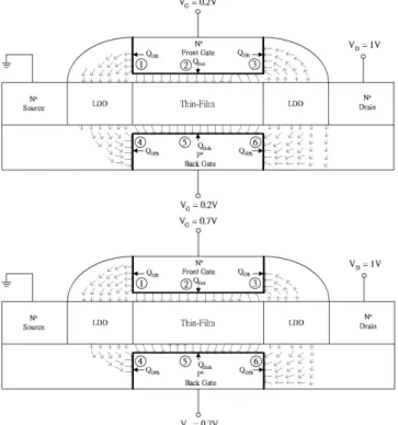
Fig. 1 Cross section of the 100nm DG FD SOI NMOS device with the n+/p+ poly top/bottom gate structure under study.
Fig. 1 shows the cross section of the 100nm DG FD SOI NMOS device under study. As shown in the figure, it has an n+/p+ poly top/bottom gate structure, a gate oxide of 3.5nm and a thin film of 50nm doped with a p-type density of 5x1017cm-3 above a buried oxide of 200nm. In addition, a 50nm LDD region with an n-type doping density of 1019 cm-3 under an oxide sidewall has been used.
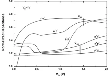
Fig. 2 CGS and CGD versus VG of the DG FD
SOI NMOS device using the n+/p+ poly top/bottom gate, biased at VD=1V.
Fig. 2 shows the source and the gate-drain capacitances (CGS/ CGD)versus the gate
voltage (VG ) of the DG FD SOI NMOS device
using the n+/p+ poly top/bottom gate, biased at the drain voltage of 1V. Also shown in the figure are the results for the device using the n+/n+ and the p+/p+ top/bottom gate structures. As shown in the figure, for the n+/n+ case, a normal capacitance behavior as for the bulk CMOS device can be seen. On the other hand, for the n+/p+ case, around the gate voltage of 0.5V, a sudden fall in the capacitance (CGS/
as compared to the capacitance characteristics for the bulk CMOS devices. A similar fall can also be observed in the CGS
characteristics of the p+/p+ case. This unique capacitance phenomenon with the sudden fall around the gate voltage of 0.5V can be explained using the analysis presented in the following section.
III. Analysis of the Capacitance Behavior
Fig. 3 2D electric field vector distribution in the 100nm DG FD SOI NMOS device with the n+/p+ poly top/bottom gate biased at VD=1V and VG=0.2V/0.7V.
In this section, the unique capacitance behavior of the DG FD SOI NMOS device with the n+/p+ poly top/bottom gate is explained. Fig. 3 shows the 2D electric field vector distribution in the 100nm DG FD SOI NMOS device with the n+/p+ poly top/bottom gate, biased at VD=1V and VG=0.2V/0.7V. Note that Fig. 1
shows the case for the device biased at VD=1V
and VG=1.5V. Among the three biasing
situations— VG=1.5V, 0.7V, and 0.2V, a similar
trend on the directions of the electric field vectors at the left and the right edges and the center portion of the top n+ poly gate can be seen. In contrast, for the bottom p+ poly gate
the situation is different. As shown in Fig. 1 for the VG=1.5V case, the electric field vectors are
mostly flowing out the left and the right edges and the center portion of the p+ poly bottom gate, which indicates positive charge on the bottom gate. It also implies that negative charge exists in the buried channel for the case with VG=1.5V. While at VG=0.2V, the
electric field vectors are flowing into the three boundaries of the p+ poly bottom gate, which means negative charge on the bottom gate and also positive charge in the buried channel. For the case with VG=0.7V, the situation is
between the two extremes.
Fig. 4 Electric field distribution surrounding the top (a) and the bottom (b) gates of the device using the n+/n+ and the n+/p+ poly top/bottom gate structures, biased at VD=1V and VG=1.5V, 0.7V, and 0.2V.
Fig. 4 shows the electric field distribution surrounding the top (a) and the bottom (b) gates of the device using the n+/n+ and the n+/p+ poly top/bottom gate structures, biased at VD=1V and VG=1.5V, 0.7V, and 0.2V. As
shown in Fig. 4(a), for both the n+/n+ and the n+/p+ cases, along the left (1), the center (2), and the right (3) edges surrounding the top n+ poly gate, for the most portion its electric field is positive, which indicates the electric field vector is flowing out of the gate. However, at the gate voltage of 0.2V, at the right edge of the top n+ poly gate near the drain, its electric field can be negative. For both the n+/n+ and the n+/p+ cases, their electric field distribution surrounding the three edges of the top n+ poly gate as shown in Fig. 4(a) is similar. On the contrary, the electric field distribution along the left (4), the center (5), and the right (6) edges surrounding the bottom poly gate varies. For the n+/p+ case, the electric field is much more negative in the center (5) near the drain of the bottom p+ poly gate as compared to the case for the top gate. In addition, even at VG=0.7V,
the electric field in the center (5) near the drain could be negative, which is contrary to the case for the top gate.
IV. Discussion
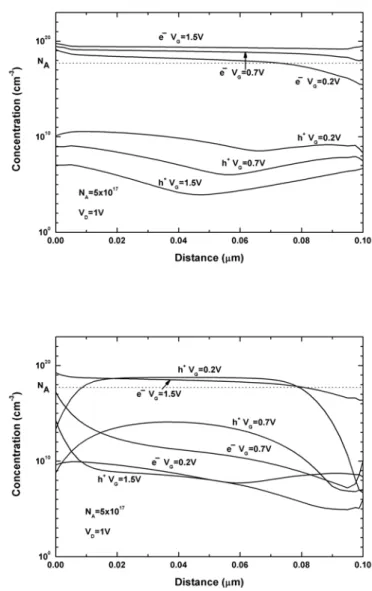
More insights into operation of the DG FD SOI NMOS device with the n+/p+ poly top/bottom gate could be obtained by looking into the carrier density distribution in the top and the bottom channels in the device. Fig. 5 shows the carrier density distribution in the top (a) and the bottom (b) lateral channels of the DG FD SOI NMOS device with the n+/p+ poly top/bottom gate biased at VD=1V and VG=1.5V,
0.7V, and 0.2V. As shown in Fig. 5(a), in the top channel under the top n+ poly gate, for the three biasing situations of VG=1.5V, 0.7V, and
0.2V, it is also with an inversion channel of electrons. In contrast, as shown in Fig. 5(b), in the bottom channel above the bottom p+ poly gate, it may have three different situations. At VG=1.5V, the electron density in the bottom
channel exceeds the p-type doping density of the thin film, which indicates the inversion channel of electrons. At VG=0.2V, the hole
density in the bottom channel surpasses the p-type doping density, which implies the accumulation of holes. At VG=0.7V, both the
electron and the hole densities in the bottom channel are smaller than the p-type doping density, which means the depletion condition of the channel. The three situations of the bottom channel— the inversion of electrons, the accumulation of holes, and the depletion condition are strongly correlated to the sudden fall of the gate-drain/source capacitance (CGD/CGS) of the DG FD SOI NMOS device
with the n+/p+ poly top/bottom gate, biased around the gate voltage of 0.5V.
Fig. 5. Carrier density distribution in the top (a) and the bottom (b) lateral channels of the DG FD SOI NMOS device with the n+/p+ poly top/bottom gate, biased at VD=1V and VG=1.5V, 0.7V, and 0.2V.
CONCLUSION
In this paper, the unique capacitance phenomenon of a 100nm DG FD SOI NMOS device with the n+/p+ poly top/bottom gate has been reported. Based on the 2D simulation result, the gate-drain/source capacitance (CGD/CGS) of the device shows a sudden fall at
the gate voltage of 0.5V due to the existence of the hole accumulation/ depletion in the bottom channel controlled by the p+ bottom gate.
ACKNOWLEDGMENT
This project is supported under R.O.C. National Science Council Grant No. 82-2218-E002-029.
REFERENCES
[1] J. B. Kuo and S. C. Lin, “Low-Voltage SOI CMOS VLSI Devices and Circuits,” Wiley,
New York, 2002.
[2] A. Vandooren, S. Cristoloveanu, and J. P. Colinge, “The Dynamic Conductance and Transconductance in Double-Gate (Gate-All-Around) SOI Devices,” SOI Conf. Proc., pp. 116-117, 2000.
[3] D. Hisamoto, “FD/DG-SOI MOSFET-A Variable Approach to Overcoming the Device Scaling Limit,” IEDM Dig., 2001. [4] K. Suzuki and T. Sugii, “Analytical Models
for n+p+ Double-Gate SOI MOSFET’s,”
IEEE Trans. Electron Devices,