torted, while the replica pulse at +3.9 ps is broad- ened and suppressed. Similar results are obtained from simulation using the actual nonlinear spec- tral dispersion function.
5. Conclusion
We have demonstrated the importance of the nonlinear distribution of pixels in the frequency domain for broadband pulse shaping. In particu- lar, we have shown that this nonlinear distribu- tion can strongly affect replica pulses arising in LCM based pulse shaping and can be used to suppress their intensity.
6. Reference I.
2. 3. 4.
A.M. Weiner, Prog. Quantum Electron. 19,
A.M. Weiner, Rev. Sci. Inst. 71, 1929(2000). M.M. Wefers, K.A. Nelson, Opt. Lett. 20, (9)
A.M. Weiner, D.E. Leaird, J.S. Patel and J.R. Wullert, IEEE J. Quantum Electron., vol. 28, 908 (1992).
5. P.F. McManamon, T.A. Dorschner, D.L. Corkum, L.J. Friedman, D.S. Hobbs, M. Hob, S. Liberman, H.Q. Nguyen, D.P. Resler, R.C. Sharp, E.A. Watson, IEEE Proc. 84, (2)
L. Wang, A.M. Weiner, Opt. Comm., 167, 161-238 (1995). 1047-1049 (1995). 268-298,1996. 6. 211-224 (1999). ~~~~~
CTuV
4:45
pm-6:30pm
Room
318/320
TelecomComponents
David A. Ackerman, Bell Labs., Lucent Tech., USA, Presider
CTuVl (Tutorial) 4 4 5 pm Semiconductor Lasers for WDM Systems Paul A. Morton, CIENA Corporation
This tutorial will provide an introduction to the wide range of laser devices used in current and future commercial WDM transmission systems. The talk will start with a high level description of WDM systems (Metro and Long-Haul), and point out the various classes of lasers used for each application. This will be followed by a more in-depth description of the different devices, and their important performance parameters. The talk will try to cover all types of lasers, including; i) Low Cost modules for the client interfaces of WDM systems: Transceivers, Transponders, Parallel Optics (using VCSEL transmitter ar- rays for low cost system interconnects). ii) Sources for WDM transport, including di-
rectly modulated DFB’s Integrated DFBlEA modulators, CW lasers
+
Lithium Niobate modulators, Tunable lasers-for use at 2.5G, 10G, 40G, then in the future 100G/160G? iii) Pump lasers for EDFA’s and Raman Amplifi-cation, from low costllow power to high per- formance devices.
The final section of the talk will look towards the future, describing new devices to be used in the coming years and major trends seen for com- ponents and integrated modules.
Biography
Paul Morton was born in Stockton-on-Tees in the North-East of England. He received his B.Sc., M.Eng. and Ph.D. in E.E. from the University of Bath. He moved to the USA in 1988 as a postdoc- toral researcher at U.C. Santa Barbara, then to AT&T Bell laboratories, Murray Hill, where he carried out research on high performance lasers. He interned at the Optoelectronics Business Unit (then Lucent) to learn the business of making and selling lasers. Paul moved to CIENA in 1997, where he is Director of Active Photonic Compo- nents, leading a team which carries out R&D on lasers and qualifies them for use in CIENA sys- tems. He also leads the CIENA 40G technology project.
TUESDAY AFTERNOON
/
CLEO 2001/
237
CTuV2 5 4 5 pm
Extremely Broadband Tunable Semiconductor Lasers for Optical Communication
Ching-Fuh Lin,Yi-Shin Su, and Bing-Ruey Wu, Department of Electrical Engineering And Graduate Institute of Electro-Optical Engineering, National Taiwan University, Taipei 106, Taiwan ROC; Email: cflin@cc.ee.ntu.edu.tw
1. introduction
Broadband characteristics are important for op- tical communication. Thus, many efforts are de- voted to expanding bandwidth. Recent technolo- gy has made optical fibers exhibit extremely broad bandwidth, covering nearly from 1200 nm to 1600 nm with the loss less than 0.5dBlkm.I However, The abundant bandwidth of fibers is still far from being fully exploited even with the bandwidth of Er-doped fiber amplifiers and lasers expanded from C-band (1525 nm to 1565 nm) to L-Band (1570 nm to 1610 nm). Semicon- ductor laserslamplifiers using multiple-quan- tum-well (MQW) engineering,z4 thus provide alternatives other than Er-doped fiber for the broadband purpose. This work reports the study on the design of MQWs for broadband semicon- ductor laserslamplifiers. The study shows that, with properly designed sequence of nonidentical MQWs made of InGaAsPlInP materials, the emission bandwidth could be nearly 300 nm. Us- ing the designed MQWs as the laser gain materi- al, the external-cavity semiconductor laser ex- hibits an extremely broadband tuning range, covering from 1300 nm to 1540 nm.
2. Experiment-Device Fabrication and Emission Spectrum
The designed quantum-well structure for broad- band purpose has two Ino.,3Ga,,47As QWs near the n-cladding layer and three Ino.67Gao.33 Aso.7ZPo.zs QWs near the p-cladding layer. The quantum wells are separated by wide Ino.s6Gao.lr Aso.3Po.7 barriers. The quantum-well struc- ture was grown using MOCVD. Bent-stripe ridge-waveguide semiconductor-laser amplifiers (SLA’s) were fabricated on those substrates? The device length is about 500 pm. Typical processing techniques were used for the device fabrication. The ridge waveguide was created by RIE. No facet coatings were applied to the devices.
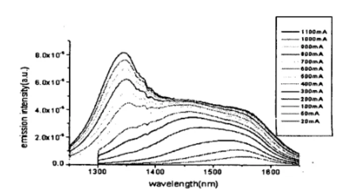
Fig. 1 shows the measured emission spectra of the fabricated SLA’s at different injection cur- rents. The emission at the low injection current occurs at the wavelength corresponding to then = 1 transition in the Ino,53G~47As QWs. The emis- sion contribution from the Ino.67Gao.33Aso.72Po.zs QW is not obvious until the injection current in- creased to above 300mA. The measurement shows that the emission bandwidth could be nearly 300 nm, covering from less than 1300 nm to over 1550 nm. Even broader bandwidth is still possible by increasing the injection current or fine tune of the QW width.
3. Experiment-Tuning Range
The above SLA is used in the external cavity for tuning experiment. Fig. 2 shows the setup of the external-cavity semiconductor laser. The grating is
AI
coated with 600 lineslmm. With the broad gain bandwidth, the semiconductor laser has an extremely broadband tuning range. It covers from 1300 nm to 1540 nm, which could serve asthe complementary to the Er-doped fiber laser to explore the broad bandwidth of fibers for optical communication. For low-injection current, the tuning range mainly lies around 1500 nm. In- creasing the injection current, the tuning range gradually extends to the 1300 nm band. The tun- ing behavior corresponds to the emission spectra shown in Fig. 1 pretty well. Fig. 3 shows the tun- ing spectra at different wavelengths. The broad- band tuning range also indicates that almost the entire emission spectrum shown in Fig. 1 could serve as the gain for laser oscillation and so should also be useful for amplification purpose. Even broader tuning range is expected with fine adjustment of lasing conditions or better de- signed MQW structures.
wavelength(nm)
230
/
CLEO
2001
/
TUESDAY AFTERNOON
SLA
C’hV2 Fig. 2. The setup of tuning experi- ment using external-cavity configuration.
m
13w 13XI Iva 14%m
lm
If433wa”clcn5th<run)
CTuV2 Fig. 3. Tuning spectra at different wavelengths (linear scale).
References
1. Stern, T.E. and Bala, K.: ‘Multiewavelength Optical Networks’, Chap. 4, pp. 193-199, Ad- dison-Wesley, MA, 1999.
Ching-Fuh Lin, Bor-Lin Lee, and Po-Chien Lin, IEEE Photon. Technol. Lett. 8, 1456 ( 1996).
X. Zhu, D.T. Cassidy, M.J. Hamp, D.A. Thompson, B.J. Robinson, Q.C. Zhao, and M. Davies, IEEE Photon. Technol. Lett.9,1202 (1997).
4. Bor-Lin Lee and Ching-Fuh Lin, CLEO/QELS’97, Baltimore, USA, Paper CThA4,1997.
5 . A.T. Semenov, V.R. Shidlovski, and S.A. Safin, Electron. Lett., Vol. 29,854 (1993). 2.
3.
CTuV3 6:OO pm
Wideband integrated multiple laser chip on 1.55 pm heterostructure using controlled bandgap tuning by quantum well intermixing
V. Aimez, J. Beauvais, J. Beerens, H.S. Lim,* And B.S. Ooi,“* Centre de Recherche sur les Propridtds Electroniques de Matbriawc Avancbs, Electrical Engineering Department and Physics Department, University of Sherbrooke, Sherbrooke, Qudbec, Canada J l K 2Rl; *Photonics Research Group, School of Electrical and Electronic Engineering, Nanyang Technological University, Singapore 639798; **Phosistor Technologies Inc, 60 Fenton Street, Livermore CA 94550
The ongoing growth of telecommunication net- work capacity requires complex optical systems for DWDM applications. With new systems be- ing developed for C and L band, the number of new high performance devices is increasing sig- nificantly. Post growth processing techniques for wide bandgap tuning of 1.55 pm wafers are an attractive approach for the fabrication of higher performance, monolithically integrated lasers and modulators. Quantum well intermix- ing (QWI) is a key technology for the fabrication of advanced photonic integrated components
(PICs) requiring integration of multiple bandgap values over a 150 nm range on a single sub- strate.’,2 The QWI technique used for this work relies on the use of a low energy ion implanter, which is an apparatus commonly available in the industry. Shallow ion implantation is carried out to generate point defects near the surface of the material, i.e. well away from the active region. Following ion implantation, rapid thermal an- nealing is carried out to reduce implantation damage and to promote intermixing of quantum wells and barriers through point defect diffusion underneath the implanted regions. After interdif- fusion, the bandgap profile of the material is in- creased so that the effective emission wavelength of processed devices is blueshifted by an amount directly related to the implantation dose. Stan- dard MOCVD-grown, 1.55 p m heterostructures with five quantum wells were used for this work. Using arsenic ion implantation, at a dose of 1.5 x 10l2 ions/cm2 with an energy of 360 keV, we have fabricated laser diodes whose characteristics are almost identical to as-grown devices (see fig. l), except for a 26 nm blueshift in the emission wavelength (see fig. 2). We have also carefully checked that the annealing step alone did not have any effect on the unimplanted material, which is a key requirement for monolithic inte- gration of multiple bandgap devices. To obtain a spatial selectivity over the blueshifting induced in our procedure, we used a variable thickness Si02 implantation mask that was photolithographi- cally defined in a single step on the substrate. De- pending on the specific region of the substrate,
o . o m - 0.0315- i - c 0.0010- I -
. . .
I: J o.om5- I , . , . , . , . , . , . , 0 . M 0.08 0.10 0.12 0.14 0.(8 0.18 0.20lnjedion current (A)
CTuV3 Fig. 1. Light versus current intensity curves from 1.5 x 10l2 ions/cm2 implanted oxide stripe laser devices (a), annealed only (b) and ref- erence devices (c).
1515 1M 1 5 P ($30 ,535 I640 <SI5 l s s 0 ISSS
Wavelength in nm
CTuV3 Fig. 2. Normalised lasing spectra from 1.5 x 10” ions/cm2 implanted oxide stripe laser devices (a), annealed only (b) and reference devices (c).
CTuV3 Fig. 3. Normalised lasing spectra from the ten channel monolithic laser devices.
the thickness of the implantation mask took one out of ten values covering the range from com- plete transparency up to full stopping of ions. Phosphorus ion implantation, at a dose of 1 x 10¹⁴ ionslcm’ with an energy of 360 k e y was then carried out followed by a rapid thermal an- nealing step. The electroluminescence spectra from the ten channel monolithic devices are shown in fig. 3. The integrated devices emission wavelength range extends over 80 nm, which covers the equivalent of the ITU’ grid wave- lengths (C band). The variation in the threshold current density among the devices was found to be limited to only about 17% (going from 1.2 kA/cm2 to 1.4 kA/cmZ).
In conclusion we have shown that low energy ion implantation induced QWI is an attractive method for post growth single step multiple bandgap tuning of high quality active and passive devices as well as PICs.
References
1. H.E. Li, “Quantum well intermixing: From visible to far-IR wavelength applications”, Design, Fabrication, and Characterization of Photonic devices conference, SPIE Vol. 3896, p 172-183,1999.
J.H. Marsh, O.P. Kowalski, S.D. McDougall, B.C. Qiu, A. McKee, C.J. Hamilton, R.M. De La Rue, and A.C. Bryce, “Quantum well in- termixing in material systems for 1.5 pm”, J. Vac. Sci. Technol. A 16,2, 1998.
3. International Telecommunication Union, ITU G.692, annex A of COM 15-R67-E. 2.
CTuV4
615
pm
Monolithic fabrication of 2 x 2 crosspoint switches in InGaAs/lnAlGaAs multiple quantum wells using quantum well Intermixing
B.C. Qiu,X.F. Liu, M.L. Ke, H.K. Lee,A.C. Bryce, J.S. Aitchison and J.H. Marsh, Department of Electronics and Electrical Engineering, University of Glasgow, Glasgow GI2 8QQ, Scotland, UK Optical switching and packet routing are highly desirable functions in optical communication networks. The requirements of both a high switching speed and low insertion loss can be met using semiconductor devices. Here we re- port the monolithic integration of semiconduc- tor optical amplifiers (SOAs), electro-absorption (EA) modulators, and passive power splitters and combiners to form 2 x 2 crosspoint switches.